
Image not available
Illustrative purposes only

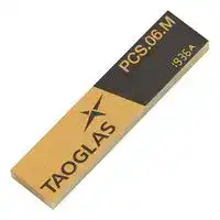
PCS.06.M
RF Antenna, 2.49 to 2.69GHz, 2G/3G/4G/Cellular/LTE /GSM/CDMA/DCS/PCS/WCDMA/UMTS/HSDPA/GPRS/EDGE
⚠️ Reference pricing provided. In case of supply shortages, we will connect you with our trusted procurement partners to ensure your project's continuity.
- Manufacturer: TAOGLAS
- Product type:
- Gain: 2.9dBi
- SVHC: To Be Advised
- VSWR: 2
- Input Power: 5W
- Antenna Type: 2G / 3G / 4G / Cellular / LTE /GSM / CDMA / DCS / PCS / WCDMA / UMTS / HSDPA / GPRS / EDGE
- Frequency Max: 2.69GHz
- Frequency Min: 2.49GHz
- Product Range: -
- Input Impedance: 50ohm
- Antenna Mounting: SMD
- Antenna Polarisation: Linear
| Delivery and price | |
|---|---|
| Units per pack | 500 |
| Price | 1.37 € |
| Current stock | 500+ |
| Lead time | 30 days |
Datasheet

## +-Qd AS A | (© +) (O C) |1.|Introduction|3| |---|---|---| |2.|Specifications|4| |3.|Antenna Characteristics|6| |4.|Radiation Patterns|9| |5.|Mechanical Drawing|18| |6.|Antenna Integration Guide|19| |7.|Packaging|27| ||Changelog|29| Taoglas makes no warranties based on the accuracy or completeness of the contents of this document and reserves the right to make changes to specifications and product descriptions at any time without notice. Taoglas reserves all rights to this document and the information contained herein. Reproduction, use or disclosure to third parties without express permission is strictly prohibited. www.taoglas.com SPE-20-8-122-C 2 ## 1. Introduction The Havok PCS.06.M is a low profile 4G Cellular SMD Dielectric embedded antenna designed for direct SMD mount on a device PCB. It provides high efficiency in a very small factor 42*10*3mm. If tuning is required it can be tuned for the device environment, while there is no need for new tooling. Its rectangular shape and very small size make it very easy to integrate – packaged in tape and reel, it can be mounted via pick and place to reflow solder directly on the edge of the PCB board. This antenna is recommended to be used with longer ground-plane lengths of 120mm or more to attain its highest rated efficiency, note the return loss and efficiency graphs in this datasheet. The PCS.06.M is a mirrored version of the standard PCS.06.A and it has been designed to operate in parallel with the PCS.06.A in a MIMO system. Typical Applications Include: - Handheld Devices - Remote Monitoring - MIMO Cellular Devices The antenna is suitable for lower cost cellular applications, especially for telematics and automotive sector. Contact your regional Taoglas customer support team for quick and professional support from our senior engineering team on integration and matching of the antenna to your device. www.taoglas.com 3 SPE-20-8-122-C ## **2.** Specifications **==> picture [39 x 42] intentionally omitted <==** ## **Electrical** |**Electrical**|**Electrical**|**Electrical**|**Electrical**|**Electrical**|**Electrical**|**Electrical**|**Electrical**| |---|---|---|---|---|---|---|---| |||**Efficiency**|**Average Gain**|**Peak Gain**|||| |**Band**|**Frequency (MHz)**||||**Impedance**|**Polarization**|**Max. input power**| |||**(%)**|**(dB)**|**(dBi)**|||| ||||||||| |**5GNR/4G**|||||||| |Band 5,8,12,13,14,17,18,20,|698~960|50|-3.1|0.5|||| |26,27,28, 29|||||||| |**5GNR/4G**|||||||| ||1427~1518|34|-4.8|1.0|||| |Band 21,32,74,75,76|||||||| ||||||||| |**4G/3G**|||||50Ω|Linear|5W| ||1710~2200|61|-2.1|3.4|||| |Band 1,2,3,4,9,23,25,35,39,66|||||||| ||||||||| |**Wi-Fi**|||||||| ||2400~2500|44|-3.5|2.6|||| |**2400**|||||||| ||||||||| |**4G/3G**|||||||| ||2490~2690|49|-3.0|2.9|||| |Band 7,38,41|||||||| ||||||||| |||**Mechanical**|||||| |**Antenna Dimensions**|42mm x 10mm x 3mm||||||| ||||||||| ||||||||| |**Material**|FR4||||||| ||||||||| ||||||||| |**Weight**|2.5g||||||| ||||||||| ||||||||| |**Soldering Type**|SMD through Reflow||||||| ||||||||| ||||||||| |**Environmental**|||||||| |**Temperature Range**|-40°C to 85°C||||||| ||||||||| ||||||||| * All measurements were done on 120*45mm EVB board with 100mm length ground plane. www.taoglas.com 4 SPE-20-8-122-C ||**5G/4G Bands**|**5G/4G Bands**|**5G/4G Bands**| |---|---|---|---| |Band Number|5GNR/FR1/LTE/LTE-Advanced/WCDMA/HSPA/HSPA+/TD-SCDMA||| ||**Uplink**|**Downlink**|**Covered**| |**1**|UL: 1920 to 1980|DL: 2110 to 2170|✓| |**2**|UL: 1850 to 1910|DL: 1930 to 1990|✓| |**3**|UL: 1710 to 1785|DL: 1805 to 1880|✓| |**4**|UL: 1710 to 1755|DL: 2110 to 2155|✓| |**5**|UL: 824 to 849|DL: 869 to 894|✓| |**7**|UL: 2500 to 2570|DL:2620 to 2690|✓| |**8**|UL: 880 to 915|DL: 925 to 960|✓| |**9**|UL: 1749.9 to 1784.9|DL: 1844.9 to 1879.9|✓| |**11**|UL: 1427.9 to 1447.9|DL: 1475.9 to 1495.9|✓| |**12**|UL: 699 to 716|DL: 729 to 746|✓| |**13**|UL: 777 to 787|DL: 746 to 756|✓| |**14**|UL: 788 to 798|DL: 758 to 768|✓| |**17**|UL: 704 to 716|DL: 734 to 746|✓| |**18**|UL: 815 to 830|DL: 860 to 875|✓| |**19**|UL: 830 to 845|DL: 875 to 890|✓| |**20**|UL: 832 to 862|DL: 791 to 821|✓| |**21**|UL: 1447.9 to 1462.9|DL: 1495.9 to 1510.9|| |**22**|UL: 3410 to 3490|DL: 3510 to 3590|| |**23**|UL:2000 to 2020|DL: 2180 to 2200|✓| |**24**|UL:1625.5 to 1660.5|DL: 1525 to 1559|| |**25**|UL: 1850 to 1915|DL: 1930 to 1995|✓| |**26**|UL: 814 to 849|DL: 859 to 894|✓| |**27**|UL: 807 to 824|DL: 852 to 869|✓| |**28**|UL: 703 to 748|DL: 758 to 803|✓| |**29**|UL: -|DL: 717 to 728|✓| |**30**|UL: 2305 to 2315|DL: 2350 to 2360|✓| |**31**|UL: 452.5 to 457.5|DL: 462.5 to 467.5|| |**32**|UL: -|DL: 1452 – 1496|| |**35**|1850 to 1910||✓| |**38**|2570 to 2620||✓| |**39**|1880 to 1920||✓| |**40**|2300 to 2400||✓| |**41**|2496 to 2690||✓| |**42**|3400 to 3600||| |**43**|3600 to 3800||| |**48**|3550 to 3700||| |**66**|UL: 1710-1780|DL: 2110-2200|✓| |**71**|617 to 698||| |**74/75/76**|1427 to 1518||| |**78**|3300 to 3800||| |**79**|4400 to 5000||| |**126**|410 to 430||| www.taoglas.com 5 SPE-20-8-122-C ## **3.** Antenna Characteristics ## **3.1** Return Loss |[4] **==> picture [448 x 262] intentionally omitted <==** **----- Start of picture text -----**<br> 0<br>-5<br>-10<br>-15<br>-20<br>-25<br>600 800 1000 1200 1400 1600 1800 2000 2200 2400 2600 2800 3000<br>Frequency [MHz]<br>Return Loss [dB]<br>**----- End of picture text -----**<br> ## **3.2** VSWR |[4] **==> picture [452 x 259] intentionally omitted <==** **----- Start of picture text -----**<br> 15.0<br>13.0<br>11.0<br>9.0<br>7.0<br>5.0<br>3.0<br>1.0<br>600 800 1000 1200 1400 1600 1800 2000 2200 2400 2600 2800 3000<br>Frequency [MHz]<br>VSWR<br>**----- End of picture text -----**<br> www.taoglas.com SPE-20-8-122-C 6 ## **3.3** Efficiency 4 **==> picture [443 x 269] intentionally omitted <==** **----- Start of picture text -----**<br> 100<br>90<br>80<br>70<br>60<br>50<br>40<br>30<br>20<br>10<br>0<br>600 800 1000 1200 1400 1600 1800 2000 2200 2400 2600 2800 3000<br>Frequency [MHz]<br>Efficiency [%]<br>**----- End of picture text -----**<br> ## **3.4** Peak Gain 4 **==> picture [443 x 278] intentionally omitted <==** **----- Start of picture text -----**<br> 4<br>2<br>0<br>-2<br>-4<br>-6<br>-8<br>-10<br>600 800 1000 1200 1400 1600 1800 2000 2200 2400 2600 2800 3000<br>Frequency [MHz]<br>Gain [dBi]<br>**----- End of picture text -----**<br> www.taoglas.com SPE-20-8-122-C 7 ## **3.5** Average Gain **==> picture [445 x 278] intentionally omitted <==** **----- Start of picture text -----**<br> 0<br>-1<br>-2<br>-3<br>-4<br>-5<br>-6<br>-7<br>-8<br>-9<br>-10<br>600 800 1000 1200 1400 1600 1800 2000 2200 2400 2600 2800 3000<br>Frequency [MHz]<br>Aver Gain [dB]<br>**----- End of picture text -----**<br> www.taoglas.com SPE-20-8-122-C 8 ## **4.** Radiation Patterns **4.** **==> picture [105 x 13] intentionally omitted <==** **----- Start of picture text -----**<br> 4.1 Test Setup<br>**----- End of picture text -----**<br> www.taoglas.com SPE-20-8-122-C 9 ## **4.2** 700MHz 3D & 2D Radiation Patterns ## XY Plane ## XZ Plane ## YZ Plane www.taoglas.com SPE-20-8-122-C 10 **==> picture [45 x 9] intentionally omitted <==** **----- Start of picture text -----**<br> 880MHz<br>**----- End of picture text -----**<br> ## XY Plane XZ Plane YZ Plane www.taoglas.com SPE-20-8-122-C 11 **==> picture [45 x 9] intentionally omitted <==** **----- Start of picture text -----**<br> 960MHz<br>**----- End of picture text -----**<br> ## XY Plane ## XZ Plane YZ Plane www.taoglas.com SPE-20-8-122-C 12 **==> picture [51 x 9] intentionally omitted <==** **----- Start of picture text -----**<br> 1700MHz<br>**----- End of picture text -----**<br> ## XY Plane ## XZ Plane ## YZ Plane www.taoglas.com SPE-20-8-122-C 13 **==> picture [51 x 9] intentionally omitted <==** **----- Start of picture text -----**<br> 1800MHz<br>**----- End of picture text -----**<br> ## XY Plane ## XZ Plane ## YZ Plane www.taoglas.com SPE-20-8-122-C 14 **==> picture [51 x 9] intentionally omitted <==** **----- Start of picture text -----**<br> 1900MHz<br>**----- End of picture text -----**<br> ## XY Plane ## XZ Plane ## YZ Plane www.taoglas.com SPE-20-8-122-C 15 **==> picture [51 x 9] intentionally omitted <==** **----- Start of picture text -----**<br> 2100MHz<br>**----- End of picture text -----**<br> ## XY Plane ## XZ Plane ## YZ Plane www.taoglas.com SPE-20-8-122-C 16 ## **2700MHz** ## XY Plane ## XZ Plane ## YZ Plane www.taoglas.com SPE-20-8-122-C 17 ## **5.** Mechanical Drawing (Units: mm) www.taoglas.com SPE-20-8-122-C 18 ## **6.** Antenna Integration Guide www.taoglas.com 19 SPE-20-8-122-C ## **6.1** Schematic Symbol and Pin Definition _ The circuit symbol for the antenna is shown below. The antenna has 4 pins with only two pins (Pin 1 and Pin 2) as functional. Pins 3 and 4 are for mechanical strength. |**Pin**<br>~~ee~~|**Description**<br>~~ee~~| |---|---| |1|RF Feed| |2|Ground| |3, 4|Mechanical, Not Connected| www.taoglas.com SPE-20-8-122-C 20 ## **6.2** Antenna Integration |[4] Whatever the size of the PCB, the antenna should ideally be placed on the PCB’s shortest side, to take advantage of the ground plane. Optimized matching components can be placed as shown. ## **6.3** PCB Layout |[4] The footprint and clearance on the PCB must meet the antenna specification. An example of the PCB layout shows the antenna footprint with clearance. Note the placement of the optimized components. L1 is positioned outside the ground plane and C1 is sitting across the ground plane and the copper clearance area. C2 is optional as a component but it is recommended to include these pads in case they are needed. Topside Bottom Side www.taoglas.com SPE-20-8-122-C 21 ## **6.4** PCB Clearance Below shows the antenna footprint and clearance through ALL layers on the PCB. Only the antenna pads and connections to feed and GND are present within this clearance area (marked RED). The clearance area extends to 5mm from the antenna mechanical pads to the ground area. This clearance area includes the bottom side and ALL internal layers on the PCB. Topside Bottom Side www.taoglas.com SPE-20-8-122-C 22 **==> picture [142 x 11] intentionally omitted <==** **----- Start of picture text -----**<br> 6.5 Evaluation Board<br>**----- End of picture text -----**<br> Top side Bottom side www.taoglas.com SPE-20-8-122-C 23 **==> picture [265 x 13] intentionally omitted <==** **----- Start of picture text -----**<br> 6.6 Evaluation Board Ground Plane Length<br>**----- End of picture text -----**<br> www.taoglas.com 24 SPE-20-8-122-C ## **6.7** Evaluation Board Matching Circuit A matching component (L1) in parallel with the PCS.06.M is required for the antenna to have optimal performance on the evaluation board, located outside of the ground plane in the space specified in the above images. C1 is also required as a matching component for this antenna. C1 is positioned sitting across the ground plane as shown in the above images. Additional matching components may be necessary for your device, so we recommend incorporating extra component footprints, forming a “pi” network, between the cellular module and the edge of the ground plane. |**Designator**|**Type**|**Value**|**Description**| |---|---|---|---| |L1|Inductor|6.8nH|TDK: MLK1005S Series| |C1|Capacitor|6.8pF|Murata:GRM1555 Series| |C2|Capacitor|Not Fitted|| www.taoglas.com SPE-20-8-122-C 25 **==> picture [298 x 610] intentionally omitted <==** **----- Start of picture text -----**<br> .7<br>6.8 Footprint<br>Toe<br>(3 TTT<br>A<br>|<br>FOOTPRINT SOLDER PADS WITH PCB OUTLINE<br>SCALE 3:1<br>1?.5 13.5<br>~<br>L +e |<br>- 4<br>1.65 | I La]<br>FOOTPRINT PCB<br>SCALE 3:]<br>I 22.5<br>g | ) =<br>b sy<br>LLLP<br>**----- End of picture text -----**<br> www.taoglas.com 26 SPE-20-8-122-C ## **7.** Packaging www.taoglas.com 27 SPE-20-8-122-C ## Changelog for the datasheet **SPE-20-8-122 – PCS.06.M** ## **Revision: C (Current Version)** Date: 2022-09-21 Notes: Updated Mechanical drawings. Author: Gary West ## **Previous Revisions** ## **Revision: B** Date: 2021-11-19 Notes: Updated data with golden sample test data & added integration guide. Author: Gary West ## **Revision: A (Original First Release)** Date: 2020-12-04 Notes: Author: Jack Conroy www.taoglas.com SPE-20-8-122-C 28 www.taoglas.com © Taoglas www.taoglas.com SPE-20-8-122-C 29
Updated at June 9, 2026
About Novapart
Novapart is a B2B electronic component broker specialising in stock shortages and cost reduction. We source hard-to-find parts and identify compliant alternatives across a catalogue of 410,000+ components from 500+ manufacturers.
Learn more →Stock Shortage Specialist
When a component is unavailable, discontinued or has an unacceptable lead time, we tap into our network of vetted European and Asian distributors to source what you need — without compromising on quality or traceability.
Request a quote →Compliant Alternatives
We identify pin-to-pin, electrically equivalent substitutes that meet the same certifications (RoHS, AEC-Q100, REACH) as your original specification — validated against datasheets, not just part numbers. Often at a lower cost.
BOM Analysis service →