
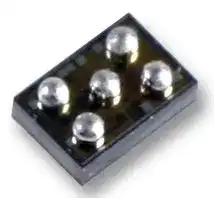


PCMF1HDMI2BA-CZ
COMMON-MODE EMI FILTER W/ESD PROTECTION
- Manufacturer: NEXPERIA
- Product type: Integrated Passive Filters
- SVHC: No SVHC (25-Jun-2025)
- No. of Pins: 5Pins
- Product Range: PCMFxHDMI2BA-C Series
- Filter Circuit: Common-Mode
- EMI Filter Type: EMI Filter with ESD Protection
- No. of Data Lines: 1 Data Lines
- Filter Case / Package: WLCSP
| Delivery and price | |
|---|---|
| Units per pack | 500 |
| Price | 0.43 € |
| Current stock | 1000+ |
| Lead time | 7 days |
## **PCMFxHDMI2BA-C series**

**Common-mode EMI filter for differential channels with integrated bidirectional ESD protection Rev. 3 — 20 May 2020**

**Product data sheet**

## **1.  General description**

Common-mode ElectroMagnetic Interference (EMI) filters with integrated bidirectional ElectroStatic Discharge (ESD) protection for one, two and three differential channels. The devices are designed to provide low insertion loss for differential high-speed signals on each channel while unwanted common-mode signals are attenuated.

Each differential channel incorporates two signal lines that are coupled by integrated coils. Diodes provide protection to downstream components from ESD voltages up to ±15 kV on each signal line.

**Table 1. Product overview**

|**Type number**|**Number of channels**|**Package Name**|
|---|---|---|
|PCMF1HDMI2BA-C|1|WLCSP5|
|PCMF2HDMI2BA-C|2|WLCSP10|
|PCMF3HDMI2BA-C|3|WLCSP15|


## **2.  Features and benefits**

- One, two and three differential channels common-mode EMI filters with integrated ESD protection

- ESD protection up to ±15 kV contact discharge according to IEC 61000-4-2

- Superior common-mode suppression over a wide frequency range

- Superior RF performance compared to other integrated filters or discrete filters with external ESD protection

- Extremely high symmetry between line pairs

- Industry-standard Wafer-Level Chip-Scale Packages: WLCSP5, 10 and 15 for smaller footprint

## **3.  Applications**

- Smartphone, cellular and cordless phone

- HDMI2.1, HDMI2.0, HDMI1.4

- General-purpose downstream ESD protection for differential data lines

- Tablet PC and Mobile Internet Device (MID)

- MIPI M-PHY and D-PHY as used in Camera Serial Interface (CSI) and Display Serial Interface (DSI)

**==> picture [140 x 35] intentionally omitted <==**

**Nexperia**

**PCMFxHDMI2BA-C series**

**Common-mode EMI filter for differential channels with integrated bidirectional ESD protection**

## **4.  Pinning information**

**Table 2. Pinning**

|**Pin**|**Symbol**|**Description**|**Simplified outline**|**Graphic symbol**|
|---|---|---|---|---|
|**PCMF1HDMI2BA-C (WLCSP5_2-1-2)**|||||
|A1|CH1_IN+|channel 1+, external|A<br>B<br>C<br>B1<br>1<br>2<br>Transparent top view<br>**WLCSP5_2-1-2**|A1<br>A2<br>C1<br>C2<br>_aaa-028492_<br>B1|
|A2|CH1_IN-|channel 1-, external|||
|B1|GND_CH1|ground channel 1|||
|C1|CH1_OUT+|channel 1+, internal|||
|C2|CH1_OUT-|channel 1-, internal|||
|**PCMF2HDMI2BA-C (WLCSP10_4-2-4)**|||||
|A1|CH1_IN+|channel 1+, external|A<br>B<br>C<br>B1<br>B2<br>1<br>2<br>3<br>4<br>Transparent top view<br>**WLCSP10_4-2-4**|_aaa-028493_<br>A1, 3<br>A2, 4<br>C1, 3<br>C2, 4<br>B1, B2 - no internal connection|
|A2|CH1_IN-|channel 1-, external|||
|A3|CH2_IN+|channel 2+, external|||
|A4|CH2_IN-|channel 2-, external|||
|B1|GND_CH1|ground channel 1|||
|B2|GND_CH2|ground channel 2|||
|C1|CH1_OUT+|channel 1+, internal|||
|C2|CH1_OUT-|channel 1-, internal|||
|C3|CH2_OUT+|channel 2+, internal|||
|C4|CH2_OUT-|channel 2-, internal|||
|**PCMF3HDMI2BA-C (WLCSP15_6-3-6)**|||||
|A1|CH1_IN+|channel 1+, external|B2<br>B3<br>B1<br>1<br>2<br>3<br>4<br>5<br>6<br>A<br>B<br>C<br>Transparent top view<br>**WLCSP15_6-3-6**|_aaa-028494_<br>B1, B2, B3 - no internal connection<br>A1, 3, 5<br>A2, 4, 6<br>C1, 3, 5<br>C2, 4, 6|
|A2|CH1_IN-|channel 1-, external|||
|A3|CH2_IN+|channel 2+, external|||
|A4|CH2_IN-|channel 2-, external|||
|A5|CH3_IN+|channel 3+, external|||
|A6|CH3_IN-|channel 3-, external|||
|B1|GND_CH1|ground channel 1|||
|B2|GND_CH2|ground channel 2|||
|B3|GND_CH3|ground channel 3|||
|C1|CH1_OUT+|channel 1+, internal|||
|C2|CH1_OUT-|channel 1-, internal|||
|C3|CH2_OUT+|channel 2+, internal|||
|C4|CH2_OUT-|channel 2-, internal|||
|C5|CH3_OUT+|channel 3+, internal|||
|C6|CH3_OUT-|channel 3-, internal|||


© Nexperia B.V. 2020. All rights reserved

PCMFXHDMI2BA_C_SER

All information provided in this document is subject to legal disclaimers.

**2 / 17**

**Rev. 3 — 20 May 2020**

**Product data sheet**

**Nexperia**

**PCMFxHDMI2BA-C series**

**Common-mode EMI filter for differential channels with integrated bidirectional ESD protection**

## **5.  Ordering information**

**Table 3. Ordering information**

|**Type number**|**Package**||
|---|---|---|
||**Name**|**Description**|
|PCMF1HDMI2BA-C|WLCSP5|wafer level chip-size package; 5 bumps (2-1-2)|
|PCMF2HDMI2BA-C|WLCSP10|wafer level chip-size package; 10 bumps (4-2-4)|
|PCMF3HDMI2BA-C|WLCSP15|wafer level chip-size package; 15 bumps (6-3-6)|


## **6.  Marking**

**Table 4. Marking codes**

|**Type number**|**Marking code**|
|---|---|
|PCMF1HDMI2BA-C|PF1A|
|PCMF2HDMI2BA-C|PF2A|
|PCMF3HDMI2BA-C|PF3A|


## **7.  Limiting values**

## **Table 5. Limiting values**

_In accordance with the Absolute Maximum Rating System (IEC 60134)._

|**Symbol**|**Parameter**|**Conditions**||**Min**|**Max**|**Unit**|
|---|---|---|---|---|---|---|
|VI|input voltage|||-4|4|V|
|VESD|electrostatic discharge<br>voltage|IEC 61000-4-2, level 4;all<br>input pins to ground|||||
|||•<br>contact discharge||-15|15|kV|
|||•<br>air discharge||-15|15|kV|
|||IEC 61000-4-2, level 4;all<br>output pins to ground|||||
|||•<br>contact discharge||-2|2|kV|
|||•<br>air discharge||-2|2|kV|
|IPPM|rated peak-pulse<br>current|tp= 8/20 μs||-7.5|7.5|A|
|Tstg|storage temperature|||-40|+125|°C|
|Tamb|ambient temperature|||-40|+125|°C|


© Nexperia B.V. 2020. All rights reserved

PCMFXHDMI2BA_C_SER

All information provided in this document is subject to legal disclaimers.

**3 / 17**

**Rev. 3 — 20 May 2020**

**Product data sheet**

**Nexperia**

**PCMFxHDMI2BA-C series**

**Common-mode EMI filter for differential channels with integrated bidirectional ESD protection**

## **8.  Characteristics**

## **8.1.  Channel characteristics**

**Table 6. Channel characteristics**

_Tamb = 25 °C unless otherwise specified._

|**Symbol**|**parameter**|**Conditions**||**Min**|**Typ**|**Max**|**Unit**|
|---|---|---|---|---|---|---|---|
|RS(ch)|channel<br>series<br>resistance|single line; input<br>to output||-|2.2|-|Ω|
|Cd|diode<br>capacitance|f = 1 MHz;<br>VI= 2.5 V|[1]|-|0.3|-|pF|
|IRM|reverse<br>leakage<br>current|per line;<br>VI= 4 V||-|1|100|nA|
|VBR|breakdown<br>voltage|IR= 1 mA||6|9|-|V|
|Rdyn|dynamic<br>resistance|TLP; positive<br>transient|[2]|-|0.29|-|Ω|
|||TLP; negative<br>transient|[2]|-|0.29|-|Ω|


[1] This parameter is guaranteed by design

[2] 100 ns Transmission Line Pulse (TLP); 50 Ω; pulser at 70 ns to 90 ns.

## **8.2.  Frequency characteristics**

**Table 7. Frequency characteristics**

_Tamb = 25 °C unless otherwise specified._

|**Symbol**|**Parameter**|**Conditions**||**Min**|**Typ**|**Max**|**Unit**|
|---|---|---|---|---|---|---|---|
|**Differential mode: Sdd21**||||||||
|f-3dB|cut-off frequency||[1]|-|10|-|GHz|


[1] Normalized to attenuation at 1 MHz.

© Nexperia B.V. 2020. All rights reserved

PCMFXHDMI2BA_C_SER

All information provided in this document is subject to legal disclaimers.

**4 / 17**

**Rev. 3 — 20 May 2020**

**Product data sheet**

**Nexperia**

**PCMFxHDMI2BA-C series**

**Common-mode EMI filter for differential channels with integrated bidirectional ESD protection**

**==> picture [238 x 207] intentionally omitted <==**

**----- Start of picture text -----**<br>
aaa-029770<br>0<br>Sdd21<br>(dB)<br>-2<br>-4<br>-6<br>10 [7] 10 [8] 10 [9] 10 [10] 10 [11]<br>f (Hz)<br>Fig. 1. Differential mode insertion loss; typical values<br>**----- End of picture text -----**<br>


**==> picture [238 x 220] intentionally omitted <==**

**----- Start of picture text -----**<br>
aaa-029772<br>0<br>Sdd21<br>(dB)<br>-20<br>-40<br>-60<br>-80<br>10 [8] 10 [9] 10 [10] 10 [11]<br>f (Hz)<br>CH1 to CH2<br>Fig. 3. Differential crosstalk; typical values<br>**----- End of picture text -----**<br>


**==> picture [233 x 189] intentionally omitted <==**

**----- Start of picture text -----**<br>
aaa-029771<br>0<br>Scc21<br>(dB)<br>-10<br>-20<br>-30<br>-40<br>10 [7] 10 [8] 10 [9] 10 [10] 10 [11]<br>f (Hz)<br>**----- End of picture text -----**<br>


**Fig. 2. Common-mode insertion loss; typical values**

**==> picture [233 x 204] intentionally omitted <==**

**----- Start of picture text -----**<br>
aaa-029773<br>115<br>Zdif<br>(Ω)<br>105<br>Z reference<br>95<br>Z DUT<br>85<br>44.2 44.4 44.6 44.8<br>t (ns)<br>tr = 200 ps<br>**----- End of picture text -----**<br>


**Fig. 4. Differential Time Domain Reflectometer (TDR) plot; typical values**

© Nexperia B.V. 2020. All rights reserved

PCMFXHDMI2BA_C_SER

All information provided in this document is subject to legal disclaimers.

**5 / 17**

**Rev. 3 — 20 May 2020**

**Product data sheet**

**Nexperia**

**PCMFxHDMI2BA-C series**

**Common-mode EMI filter for differential channels with integrated bidirectional ESD protection**

Short cable model (SCM), no equalizer

- **Fig. 5. HDMI 2.1 12G FRL eye diagram, PCB with device; typical values**

Short cable model (SCM), no equalizer

**Fig. 6. HDMI 2.1 12G FRL eye diagram, PCB without device; typical values**

© Nexperia B.V. 2020. All rights reserved

PCMFXHDMI2BA_C_SER

All information provided in this document is subject to legal disclaimers.

**6 / 17**

**Rev. 3 — 20 May 2020**

**Product data sheet**

**Nexperia**

**PCMFxHDMI2BA-C series**

**Common-mode EMI filter for differential channels with integrated bidirectional ESD protection**

Worst cable model, 8dB

- **Fig. 7. HDMI 2.1 12G FRL eye diagram, PCB with device; typical values**

## Worst cable model, 8dB

**Fig. 8. HDMI 2.1 12G FRL eye diagram, PCB without device; typical values**

© Nexperia B.V. 2020. All rights reserved

PCMFXHDMI2BA_C_SER

All information provided in this document is subject to legal disclaimers.

**7 / 17**

**Rev. 3 — 20 May 2020**

**Product data sheet**

**Nexperia**

**PCMFxHDMI2BA-C series**

**Common-mode EMI filter for differential channels with integrated bidirectional ESD protection**

Worst cable model, no equalizer

**Fig. 9. HDMI 2.1 6 Gbps TMDS eye diagram, PCB with device; typical values**

Worst cable model, no equalizer

**Fig. 10. HDMI 2.1 6 Gbps TMDS eye diagram, PCB without device; typical values**

© Nexperia B.V. 2020. All rights reserved

PCMFXHDMI2BA_C_SER

All information provided in this document is subject to legal disclaimers.

**8 / 17**

**Rev. 3 — 20 May 2020**

**Product data sheet**

**Nexperia**

**PCMFxHDMI2BA-C series**

## **Common-mode EMI filter for differential channels with integrated bidirectional ESD protection**

**==> picture [497 x 512] intentionally omitted <==**

**----- Start of picture text -----**<br>
aaa-029774 aaa-029775<br>25 0<br>I I<br>(A) (A)<br>20 -5<br>15 -10<br>10 -15<br>5 -20<br>0 -25<br>0 4 8 12 16 -16 -12 -8 -4 0<br>VCL (V) VCL (V)<br>Transmission Line Pulse (TLP) = 100 ns; Transmission Line Pulse (TLP) = 100 ns;<br>measured CH_IN to GND measured CH_IN to GND<br>Fig. 11. Dynamic resistance with positive clamping; Fig. 12. Dynamic resistance with negative clamping;<br>typical values typical values<br>aaa-029776 aaa-029777<br>60 0<br>I I<br>(A) (A)<br>40 -20<br>20 -40<br>0 -60<br>0 10 20 30 -30 -20 -10 0<br>VCL (V) VCL (V)<br>Very-Fast Transmission Line Pulse Very-Fast Transmission Line Pulse<br>(VF-TLP) = 5 ns; (VF-TLP) = 5 ns;<br>measured CH_IN to GND measured CH_IN to GND<br>Fig. 13. Dynamic resistance with positive clamping; Fig. 14. Dynamic resistance with negative clamping;<br>typical values typical values<br>**----- End of picture text -----**<br>


The device uses an advanced clamping structure showing a negative dynamic resistance. This snap-back behavior strongly reduces the clamping voltage to the system behind the ESD protection during an ESD event. Do not connect unlimited DC current sources to the data lines to avoid keeping the ESD protection device in snap-back state after exceeding breakdown voltage (due to an ESD pulse for instance).

© Nexperia B.V. 2020. All rights reserved

PCMFXHDMI2BA_C_SER

All information provided in this document is subject to legal disclaimers.

**9 / 17**

**Rev. 3 — 20 May 2020**

**Product data sheet**

**Nexperia**

**PCMFxHDMI2BA-C series**

## **Common-mode EMI filter for differential channels with integrated bidirectional ESD protection**

**==> picture [497 x 238] intentionally omitted <==**

**----- Start of picture text -----**<br>
aaa-029778 aaa-029779<br>8 0<br>I I<br>(A) (A)<br>6 -2<br>4 -4<br>2 -6<br>0 -8<br>0 2 4 6 8 -8 -6 -4 -2 0<br>VCL (V) VCL (V)<br>IEC61000-4-5; tp = 8/20 μs; positive pulse IEC61000-4-5; tp = 8/20 μs; negative pulse<br>Fig. 15. Dynamic resistance with positive clamping; Fig. 16. Dynamic resistance with negative clamping;<br>typical values typical values<br>**----- End of picture text -----**<br>


## **9.  Application information**

The device is designed to provide high-level ESD protection for differential high-speed data line pairs such as HDMI2.1, HDMI2.0 and HDMI1.4.

When designing the Printed-Circuit Board (PCB), give careful consideration to impedance matching and signal coupling. Do not connect the protected signal lines to unlimited current sources like, for example, a battery.

© Nexperia B.V. 2020. All rights reserved

PCMFXHDMI2BA_C_SER

All information provided in this document is subject to legal disclaimers.

**10 / 17**

**Rev. 3 — 20 May 2020**

**Product data sheet**

**Nexperia**

**PCMFxHDMI2BA-C series**

**Common-mode EMI filter for differential channels with integrated bidirectional ESD protection**

## **10.  Package outline**

**==> picture [486 x 593] intentionally omitted <==**

**----- Start of picture text -----**<br>
WLCSP5: wafer level chip-size package; 5 bumps (2-1-2) PCMF1HDMI2BA/C<br>D<br>bump A1<br>index area A1<br>E A<br>detail X<br>e<br>1/2 e<br>b<br>C<br>e1<br>B1<br>B e2<br>A<br>bump A1 1 2<br>index area<br>X<br>0 1 mm<br>scale<br>Dimensions (mm are the original dimensions)<br>Unit A A1 b D E e e1 e2<br>max 0.64 0.42 0.31 0.82 1.22<br>mm nom 0.61 0.41 0.26 0.77 1.17 0.40 0.40 0.80<br>min 0.58 0.40 0.21 0.72 1.12<br>pcmf1hdmi2ba-c_po<br>Outline References European Issue date<br>version IEC JEDEC JEITA projection<br>20-05-06<br>PCMF1HDMI2BA/C<br>Fig. 17. Package outline WLCSP5<br>**----- End of picture text -----**<br>


© Nexperia B.V. 2020. All rights reserved

PCMFXHDMI2BA_C_SER

All information provided in this document is subject to legal disclaimers.

**11 / 17**

**Rev. 3 — 20 May 2020**

**Product data sheet**

**Nexperia**

**PCMFxHDMI2BA-C series**

**Common-mode EMI filter for differential channels with integrated bidirectional ESD protection**

**WLCSP10: wafer level chip-size package; 10 bumps (4-2-4)**

## **PCMF2HDMI2BA/C**

**==> picture [481 x 565] intentionally omitted <==**

**----- Start of picture text -----**<br>
D<br>bump A1index area A1<br>E A<br>detail X<br>e b<br>C<br>e1<br>B1 B2<br>B e2<br>A<br>bump A1 1 2 3 4<br>index area e3 X<br>1/2 e<br>0 1 mm<br>scale<br>Dimensions (mm are the original dimensions)<br>Unit A A1 b D E e e1 e2 e3<br>max 0.64 0.42 0.31 1.62 1.22<br>mm nom 0.61 0.41 0.26 1.57 1.17 0.40 0.40 0.80 0.80<br>min 0.58 0.40 0.21 1.52 1.12<br>pcmf2hdmi2ba-c_po<br>Outline References European Issue date<br>version IEC JEDEC JEITA projection<br>20-05-06<br>PCMF2HDMI2BA/C<br>**----- End of picture text -----**<br>


**Fig. 18. Package outline WLCSP10**

© Nexperia B.V. 2020. All rights reserved

PCMFXHDMI2BA_C_SER

All information provided in this document is subject to legal disclaimers.

**12 / 17**

**Rev. 3 — 20 May 2020**

**Product data sheet**

**Nexperia**

**PCMFxHDMI2BA-C series**

**Common-mode EMI filter for differential channels with integrated bidirectional ESD protection**

**==> picture [481 x 574] intentionally omitted <==**

**----- Start of picture text -----**<br>
WLCSP15: wafer level chip-size package; 15 bumps (6-3-6) PCMF3HDMI2BA/C<br>D<br>bump A1<br>index area A1<br>E A<br>detail X<br>e 1/2 e b<br>C<br>e1<br>B B1 B2 B3 e2<br>A<br>bump A1 1 2 3 4 5 6<br>index area e3 X<br>0 1 mm<br>scale<br>Dimensions (mm are the original dimensions)<br>Unit A A1 b D E e e1 e2 e3<br>max 0.64 0.42 0.31 2.42 1.22<br>mm nom 0.61 0.41 0.26 2.37 1.17 0.40 0.40 0.80 0.80<br>min 0.58 0.40 0.21 2.32 1.12<br>pcmf3hdmi2ba-c_po<br>Outline References European Issue date<br>version IEC JEDEC JEITA projection<br>20-05-06<br>PCMF3HDMI2BA/C<br>**----- End of picture text -----**<br>


**Fig. 19. Package outline WLCSP15**

© Nexperia B.V. 2020. All rights reserved

PCMFXHDMI2BA_C_SER

All information provided in this document is subject to legal disclaimers.

**13 / 17**

**Rev. 3 — 20 May 2020**

**Product data sheet**

**Nexperia**

**PCMFxHDMI2BA-C series**

**Common-mode EMI filter for differential channels with integrated bidirectional ESD protection**

## **11.  Soldering**

**==> picture [481 x 266] intentionally omitted <==**

**----- Start of picture text -----**<br>
WLCSP5: Solder footprint and stencil aperture PCMF1HDMI2BA/C<br>Hx<br>P<br>see<br>detail X<br>P<br>solder land (SL)<br>Hy<br>solder paste deposit (SP)<br>solder land plus solder paste<br>SL = SP<br>solder resist opening (SR)<br>SR<br>occupied area<br>detail X<br>Dimensions in mm<br>recommend stencil thickness: 0.1 mm<br>P SL SP SR Hx Hy<br>0.40 0.25 0.25 0.325 1.00 1.40 20-05-06<br>pcmf1hdmi2ba-c_fr<br>**----- End of picture text -----**<br>


**Fig. 20. Soldering footprint WLCSP5 (PCMF1HDMI2BA/C)**

**WLCSP10: Solder footprint and stencil aperture**

**==> picture [73 x 6] intentionally omitted <==**

**----- Start of picture text -----**<br>
PCMF2HDMI2BA/C<br>**----- End of picture text -----**<br>


**==> picture [481 x 256] intentionally omitted <==**

**----- Start of picture text -----**<br>
Hx<br>P<br>see<br>detail X<br>P<br>solder land (SL)<br>Hy<br>solder paste deposit (SP)<br>solder land plus solder paste<br>SL = SP<br>solder resist opening (SR)<br>SR<br>occupied area<br>P1 detail X<br>Dimensions in mm<br>recommend stencil thickness: 0.1 mm<br>P P1 SL SP SR Hx Hy<br>0.40 0.80 0.25 0.25 0.325 1.80 1.40 20-05-06<br>pcmf2hdmi2ba-c_fr<br>**----- End of picture text -----**<br>


**Fig. 21. Soldering footprint WLCSP10 (PCMF2HDMI2BA/C)**

© Nexperia B.V. 2020. All rights reserved

PCMFXHDMI2BA_C_SER

All information provided in this document is subject to legal disclaimers.

**14 / 17**

**Rev. 3 — 20 May 2020**

**Product data sheet**

**Nexperia**

**PCMFxHDMI2BA-C series**

**Common-mode EMI filter for differential channels with integrated bidirectional ESD protection**

**==> picture [481 x 266] intentionally omitted <==**

**----- Start of picture text -----**<br>
WLCSP15: Solder footprint and stencil aperture PCMF3HDMI2BA/C<br>Hx<br>P<br>see<br>detail X<br>P<br>solder land (SL)<br>Hy<br>solder paste deposit (SP)<br>solder land plus solder paste<br>SL = SP<br>solder resist opening (SR)<br>SR<br>occupied area<br>P1 detail X<br>Dimensions in mm<br>recommend stencil thickness: 0.1 mm<br>P P1 SL SP SR Hx Hy<br>0.40 0.80 0.25 0.25 0.325 2.60 1.40 20-05-06<br>pcmf3hdmi2ba-c_fr<br>**----- End of picture text -----**<br>


**Fig. 22. Soldering footprint WLCSP15 (PCMF3HDMI2BA/C)**

© Nexperia B.V. 2020. All rights reserved

PCMFXHDMI2BA_C_SER

All information provided in this document is subject to legal disclaimers.

**15 / 17**

**Rev. 3 — 20 May 2020**

**Product data sheet**

**Nexperia**

**PCMFxHDMI2BA-C series**

**Common-mode EMI filter for differential channels with integrated bidirectional ESD protection**

## **12.  Revision history**

## **Table 8. Revision history**

|**Document ID**|**Release**<br>**date**|**Data sheet status**|**Change**<br>**notice**|**Supersedes**|
|---|---|---|---|---|
|PCMFXHDMI2BA_C_SER v.1|20200520|Product data sheet|-|-|


© Nexperia B.V. 2020. All rights reserved

PCMFXHDMI2BA_C_SER **Product data sheet**

All information provided in this document is subject to legal disclaimers.

**16 / 17**

**Rev. 3 — 20 May 2020**

**Nexperia**

**PCMFxHDMI2BA-C series**

**Common-mode EMI filter for differential channels with integrated bidirectional ESD protection**

## **Contents**

**1.  General description......................................................1 2.  Features and benefits.................................................. 1 3.  Applications.................................................................. 1 4.  Pinning information......................................................2 5.  Ordering information....................................................3 6.  Marking..........................................................................3 7.  Limiting values............................................................. 3 8.  Characteristics..............................................................4** 8.1.  Channel characteristics............................................... 4 8.2.  Frequency characteristics............................................4 **9.  Application information............................................. 10 10.  Package outline........................................................ 11 11.  Soldering................................................................... 14 12.  Revision history........................................................16**

## © **Nexperia B.V. 2020. All rights reserved**

For more information, please visit: http://www.nexperia.com For sales office addresses, please send an email to: salesaddresses@nexperia.com **Date of release: 20 May 2020**

© Nexperia B.V. 2020. All rights reserved

PCMFXHDMI2BA_C_SER

All information provided in this document is subject to legal disclaimers.

**17 / 17**

**Rev. 3 — 20 May 2020**

**Product data sheet**
Updated at March 17, 2026
Nexperia is a dedicated global leader in discretes, logic, and MOSFET devices. Built on over half a century of semiconductor expertise and operating independently since 2017, the company produces consistently reliable components at an exceptional volume of 85 billion units annually. With its own manufacturing facilities, Nexperia delivers industry-leading small packages that combine power and thermal efficiency with best-in-class quality, meeting the rigorous standards of the automotive sector. Our extensive Nexperia portfolio is heavily focused on discrete semiconductors, providing engineers with a robust selection of core building blocks. This includes a comprehensive range of diodes and rectifiers, featuring a vast selection of Zener single diodes and Schottky diodes designed for precise voltage regulation and efficient power routing. Additionally, we offer an expansive array of bipolar transistors and single MOSFETs tailored for reliable switching and amplification in demanding applications. Beyond these primary offerings, the lineup extends into specialized circuit protection and passive components. This includes transient voltage suppressor (TVS) diodes, Zener array diodes, and small signal diodes, alongside dual MOSFETs and fast recovery rectifiers. For comprehensive design needs, the selection also encompasses integrated passive filters, common mode chokes, and precision timers and oscillators, ensuring a complete solution for high-performance electronic systems.
About Novapart
Novapart is a B2B electronic component broker specialising in stock shortages and cost reduction. We source hard-to-find parts and identify compliant alternatives across a catalogue of 410,000+ components from 500+ manufacturers.
Learn more →Stock Shortage Specialist
When a component is unavailable, discontinued or has an unacceptable lead time, we tap into our network of vetted European and Asian distributors to source what you need — without compromising on quality or traceability.
Request a quote →Compliant Alternatives
We identify pin-to-pin, electrically equivalent substitutes that meet the same certifications (RoHS, AEC-Q100, REACH) as your original specification — validated against datasheets, not just part numbers. Often at a lower cost.
BOM Analysis service →