


PB5010-E3/45
Bridge Rectifier, Single Phase, 1 kV, 45 A, SIP, 4 Pins, 1.1 V
- Manufacturer: VISHAY
- Product type: Bridge Rectifier Diodes
- No. of Phases:Single Phase; Repetitive Reverse Voltage Vrrm Max:1kV; Forward Current If(AV):45A; Bridge Rectifier Case Style:SIP; Forward Voltage VF Max:1.1V; No. of Pins:4Pins; Operati
- SVHC: Lead (04-Feb-2026)
- No. of Pins: 4Pins
- No. of Phases: Single Phase
- Product Range: PB501
- Forward Voltage Max: 1.1V
- Forward Surge Current: 450A
- Average Forward Current: 45A
- Bridge Rectifier Mounting: Through Hole
- Operating Temperature Max: 150°C
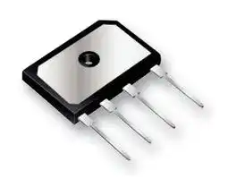
- Bridge Rectifier Case Style: SIP
- Repetitive Peak Reverse Voltage: 1kV
| Delivery and price | |
|---|---|
| Units per pack | 1000 |
| Price | 1.52 € |
| Current stock | 1000+ |
| Lead time | 30 days |
## **PB5006, PB5008, PB5010** www.vishay.com Vishay General Semiconductor “ww ~~a~~ **Enhanced isoCink+[TM] Bridge Rectifiers**

**==> picture [181 x 167] intentionally omitted <==**

**----- Start of picture text -----**<br>
isoCink+™<br>’ \ 4 N<br>+<br>~ [-] GC<br>~<br>NS + SS - [~] [~]<br>Case Style PB<br>+ ~ ~ -<br>**----- End of picture text -----**<br>


*Tested to UL standard for safety electrically isolated semiconductor devices. UL 1557 4th edition. Dielectric tested to maximum case, storage and junction temperature to 150 °C to withstand 1500 V. Epoxy meets UL 94 V-0 flammability rating.

**LINKS TO ADDITIONAL RESOURCES** ~~es~~ 3D Models

## **PRIMARY CHARACTERISTICS**

## **FEATURES**

- UL recognition file number E312394 (QQQX2) UL 1557 (see *)

- Enhanced high-current density single  in-line package

- Superior thermal conductivity

- Glass passivated chip junction

- Solder dip 275 °C max. 10 s, per JESD 22-B106

- Material categorization: for definitions of compliance please see www.vishay.com/doc?99912

## **TYPICAL APPLICATIONS**

General purpose use in AC/DC bridge full wave rectification for switching power supply, home appliances and white-goods applications.

## **MECHANICAL DATA**

## **Case:** PB

Molding compound meets UL 94 V-0 flammability rating Base P/N-E3 - RoHS-compliant, industrial grade

**Terminals:** matte tin plated leads, solderable per J-STD-002 and JESD 22-B102

E3 suffix meets JESD 201 class 1A whisker test

**Polarity:** as marked on body

**Mounting Torque:** 10 cm-kg (8.8 inches-lbs) max. **Recommended Torque:** 5.7 cm-kg (5 inches-lbs)

|**PRIMARY CHARACTERISTICS**|**PRIMARY CHARACTERISTICS**|
|---|---|
|Package|PB|
|IF(AV)|45 A|
|VRRM|600 V, 800 V, 1000 V|
|IFSM|450 A|
|IR|10 μA|
|VFat IF= 22.5 A|0.90 V|
|TJmax.|150 °C|
|Circuit configuration|In-line|


## **MAXIMUM RATINGS** (TA = 25 °C unless otherwise noted)

|**MAXIMUM RATINGS**(TA = 25 °C unless otherwise noted)TA = 25 °C unless otherwise noted)A = 25 °C unless otherwise noted)= 25 °C unless otherwise noted))|**MAXIMUM RATINGS**(TA = 25 °C unless otherwise noted)TA = 25 °C unless otherwise noted)A = 25 °C unless otherwise noted)= 25 °C unless otherwise noted))|**MAXIMUM RATINGS**(TA = 25 °C unless otherwise noted)TA = 25 °C unless otherwise noted)A = 25 °C unless otherwise noted)= 25 °C unless otherwise noted))|**MAXIMUM RATINGS**(TA = 25 °C unless otherwise noted)TA = 25 °C unless otherwise noted)A = 25 °C unless otherwise noted)= 25 °C unless otherwise noted))|**MAXIMUM RATINGS**(TA = 25 °C unless otherwise noted)TA = 25 °C unless otherwise noted)A = 25 °C unless otherwise noted)= 25 °C unless otherwise noted))|**MAXIMUM RATINGS**(TA = 25 °C unless otherwise noted)TA = 25 °C unless otherwise noted)A = 25 °C unless otherwise noted)= 25 °C unless otherwise noted))|
|---|---|---|---|---|---|
|**PARAMETER**|**SYMBOL**|**PB5006**|**PB5008**|**PB5010**|**UNIT**|
|Maximum repetitive peak reverse voltage|VRRM|600|800|1000|V|
|Average rectified forward current (Fig. 1, 2)<br>TC= 84 °C(1)<br>TA= 25 °C(2)|IO|45|||A|
|||4.5||||
|Non-repetitive peak forward surge current<br>8.3 ms single sine-wave, TJ= 25 °C|IFSM|450|||A|
|Ratingfor fusing(t < 8.3 ms) TJ= 25 °C|I2t|840|||A2s|
|Operatingjunction and storage temperature range|TJ, TSTG|-55 to +150|||°C|


## **Notes**

- (1) With heatsink

> (2) Without heatsink, free air

Revision: 25-Mar-2021

Document Number: 84809

**1**

For technical questions within your region: DiodesAmericas@vishay.com, DiodesAsia@vishay.com, DiodesEurope@vishay.com THIS DOCUMENT IS SUBJECT TO CHANGE WITHOUT NOTICE. THE PRODUCTS DESCRIBED HEREIN AND THIS DOCUMENT ARE SUBJECT TO SPECIFIC DISCLAIMERS, SET FORTH AT www.vishay.com/doc?91000

**PB5006, PB5008, PB5010**

www.vishay.com

Vishay General Semiconductor

|**ELECTRICAL CHARACTERISTICS**(TA= 25 °C unless otherwise noted)|**ELECTRICAL CHARACTERISTICS**(TA= 25 °C unless otherwise noted)|**ELECTRICAL CHARACTERISTICS**(TA= 25 °C unless otherwise noted)|**ELECTRICAL CHARACTERISTICS**(TA= 25 °C unless otherwise noted)|**ELECTRICAL CHARACTERISTICS**(TA= 25 °C unless otherwise noted)|**ELECTRICAL CHARACTERISTICS**(TA= 25 °C unless otherwise noted)|**ELECTRICAL CHARACTERISTICS**(TA= 25 °C unless otherwise noted)|
|---|---|---|---|---|---|---|
|**PARAMETER**|**TEST CONDITIONS**||**SYMBOL**|**TYP.**|**MAX.**|**UNIT**|
|Maximum instantaneous forward<br>voltage per diode(1)|IF= 22.5 A|TA= 25 °C|VF|1.00|1.10|V|
|||TA= 125 °C||0.90|1.00||
|Reverse current per diode(2)|rated VR|TA= 25 °C|IR|-|10|μA|
|||TA= 125 °C||170|500||
|Typical junction capacitance per diode|4.0 V, 1 MHz||CJ|162|-|pF|


## **Notes**

- (1) Pulse test: 300 μs pulse width, 1 % duty cycle

- (2) Pulse test: 10 ms pulse width

|**THERMAL CHARACTERISTICS**(TA= 25 °C unless otherwise noted)|**THERMAL CHARACTERISTICS**(TA= 25 °C unless otherwise noted)|**THERMAL CHARACTERISTICS**(TA= 25 °C unless otherwise noted)|**THERMAL CHARACTERISTICS**(TA= 25 °C unless otherwise noted)|**THERMAL CHARACTERISTICS**(TA= 25 °C unless otherwise noted)|**THERMAL CHARACTERISTICS**(TA= 25 °C unless otherwise noted)|
|---|---|---|---|---|---|
|**PARAMETER**|**SYMBOL**|**PB5006**|**PB5008**|**PB5010**|**UNIT**|
|Typical thermal resistance|RθJC(1)|0.7|||°C/W|
||RθJA (2)|18||||


## **Notes**

- (1) With 60 W air cooled heatsink

- (2) Without heatsink, free air

## **ORDERING INFORMATION** (Example)

|**ORDERING INFORMATION**(Example)|**ORDERING INFORMATION**(Example)|**ORDERING INFORMATION**(Example)|**ORDERING INFORMATION**(Example)|**ORDERING INFORMATION**(Example)|
|---|---|---|---|---|
|**PREFERRED P/N**|**UNIT WEIGHT (g)**|**PREFERRED PACKAGE CODE**|**BASE QUANTITY**|**DELIVERY MODE**|
|PB5006-E3/45|7.62|45|20|Tube|


Revision: 25-Mar-2021

Document Number: 84809

**2**

For technical questions within your region: DiodesAmericas@vishay.com, DiodesAsia@vishay.com, DiodesEurope@vishay.com THIS DOCUMENT IS SUBJECT TO CHANGE WITHOUT NOTICE. THE PRODUCTS DESCRIBED HEREIN AND THIS DOCUMENT ARE SUBJECT TO SPECIFIC DISCLAIMERS, SET FORTH AT www.vishay.com/doc?91000

**PB5006, PB5008, PB5010**

**==> picture [77 x 10] intentionally omitted <==**

**----- Start of picture text -----**<br>
www.vishay.com<br>**----- End of picture text -----**<br>


## Vishay General Semiconductor

## **RATINGS AND CHARACTERISTICS CURVES** (TA  = 25 °C unless otherwise noted)

**==> picture [460 x 566] intentionally omitted <==**

**----- Start of picture text -----**<br>
100<br>With Heatsink TA = 150  ° C<br>Sine-Wave, R-Load<br>TA = 125 °C<br>10<br>TC TC T A  = 100 °C<br>T A  = 25 °C<br>1<br>T A  = 85 °C<br>T C Measured at Device Bottom<br>0.1<br>0.4 0.5 0.6 0.7 0.8 0.9 1.0 1.1 1.2<br>Case Temperature (°C) Instantaneous Forward Voltage (V)<br>Fig. 1 - Derating Curve Output Rectified Current Fig. 4 - Typical Forward Characteristics Per Diode<br>1000 TA = 150 °C<br>TA = 125  ° C<br>100<br>TA = 100 °C<br>10 TA = 85 °C<br>1<br>Without Heatsink Sine-Wave, R-Load 0.1 T A = 25 °C<br>Free Air, TA<br>0.01<br>10 20 30 40 50 60 70 80 90 100<br>Ambient Temperature (°C) Percent of Rated Peak Reverse Voltage (%)<br>Fig. 2 - Forward Current Derating Curve Fig. 5 - Typical Reverse Characteristics Per Diode<br>120<br>TJ = 25  ° C<br>f = 1.0 MHz<br>100 V sig  = 50 mV p-p<br>80<br>60<br>40<br>20<br>0<br>0 5 10 15 20 25 30 35 40 45 50 55<br>Average Forward Current (A) Reverse Voltage (V)<br>50<br>45<br>40<br>35<br>30<br>25<br>20<br>15<br>10<br>5<br>0<br>0 20 40 60 80 100 120 140 160<br>5<br>4<br>3<br>2<br>1<br>0<br>0 25 50 75 100 125 150<br>1000<br>100<br>10<br>0.1 1 10 100<br>Instantaneous Reverse Current (µA)<br>Forward Power Dissipation (W)<br>Instantaneous Forward Current (A)<br>Average Forward Rectified Current (A)<br>Average Forward Output Current (A)<br>Junction Capacitance (pF)<br>**----- End of picture text -----**<br>


Fig. 4 - Typical Forward Characteristics Per Diode

**==> picture [178 x 9] intentionally omitted <==**

**----- Start of picture text -----**<br>
Fig. 5 - Typical Reverse Characteristics Per Diode<br>**----- End of picture text -----**<br>


Fig. 6 - Typical Junction Capacitance Per Diode

Fig. 3 - Forward Power Dissipation

Revision: 25-Mar-2021

Document Number: 84809

**3**

For technical questions within your region: DiodesAmericas@vishay.com, DiodesAsia@vishay.com, DiodesEurope@vishay.com THIS DOCUMENT IS SUBJECT TO CHANGE WITHOUT NOTICE. THE PRODUCTS DESCRIBED HEREIN AND THIS DOCUMENT ARE SUBJECT TO SPECIFIC DISCLAIMERS, SET FORTH AT www.vishay.com/doc?91000

**PB5006, PB5008, PB5010**

**==> picture [77 x 10] intentionally omitted <==**

**----- Start of picture text -----**<br>
www.vishay.com<br>**----- End of picture text -----**<br>


## Vishay General Semiconductor

## **PACKAGE OUTLINE DIMENSIONS** in inches (millimeters)

**==> picture [61 x 9] intentionally omitted <==**

**----- Start of picture text -----**<br>
Case Type PB<br>**----- End of picture text -----**<br>


**==> picture [405 x 225] intentionally omitted <==**

**----- Start of picture text -----**<br>
Front Side View Side View<br>1.193 (30.3) 0.201 (5.1)<br>0.118 (3.0) x 45° 1.169 (29.7) 0.177 (4.5) 0.161 (4.1)<br>CHAMFER 0.138 (3.5)<br>0.799 (20.3) 0.145 (3.7) 0.134 (3.4)<br>0.130 (3.3) 0.118 (3.0)<br>0.776 (19.7)<br>0.441 (11.2)<br>0.425 (10.8) 0.205 (5.20) 120° TYP.<br>0.189 (4.80)<br>5° TYP. 5° TYP.<br>0.106 (2.70) 0.118 (3.0)<br>0.091 (2.30)<br>0.165 (4.20) 0.102 (2.6)<br>0.094 (2.40) 0.150 (3.80) 0.708 (18.0)<br>0.079 (2.00) 0.669 (17.0)<br>0.043 (1.10)<br>0.035 (0.90) 0.032 (0.80)<br>0.402 (10.2) 0.303 (7.70) 0.024 (0.60)<br>0.386 (9.80) 0.303 (7.70) 0.287 (7.30)<br>0.287 (7.30)<br>**----- End of picture text -----**<br>


**Back Side View**

**==> picture [242 x 175] intentionally omitted <==**

**----- Start of picture text -----**<br>
1.041 (26.44) REF.<br>0.070 (1.78) REF.<br>0.088 (2.24)<br>REF.<br>0.633 (16.07)<br>REF.<br>0.214 (5.44) REF.<br>0.066 (1.68)<br>REF.<br>**----- End of picture text -----**<br>


Revision: 25-Mar-2021

Document Number: 84809

**4**

For technical questions within your region: DiodesAmericas@vishay.com, DiodesAsia@vishay.com, DiodesEurope@vishay.com THIS DOCUMENT IS SUBJECT TO CHANGE WITHOUT NOTICE. THE PRODUCTS DESCRIBED HEREIN AND THIS DOCUMENT ARE SUBJECT TO SPECIFIC DISCLAIMERS, SET FORTH AT www.vishay.com/doc?91000

**Legal Disclaimer Notice** Vishay

www.vishay.com

## **Disclaimer**

ALL PRODUCT, PRODUCT SPECIFICATIONS AND DATA ARE SUBJECT TO CHANGE WITHOUT NOTICE TO IMPROVE RELIABILITY, FUNCTION OR DESIGN OR OTHERWISE.

Vishay Intertechnology, Inc., its affiliates, agents, and employees, and all persons acting on its or their behalf (collectively, “Vishay”), disclaim any and all liability for any errors, inaccuracies or incompleteness contained in any datasheet or in any other disclosure relating to any product.

Vishay makes no warranty, representation or guarantee regarding the suitability of the products for any particular purpose or the continuing production of any product.  To the maximum extent permitted by applicable law, Vishay disclaims (i) any and all liability arising out of the application or use of any product, (ii) any and all liability, including without limitation special, consequential or incidental damages, and (iii) any and all implied warranties, including warranties of fitness for particular purpose, non-infringement and merchantability.

Statements regarding the suitability of products for certain types of applications are based on Vishay’s knowledge of typical requirements that are often placed on Vishay products in generic applications.  Such statements are not binding statements about the suitability of products for a particular application.  It is the customer’s responsibility to validate that a particular product with the properties described in the product specification is suitable for use in a particular application. Parameters provided in datasheets and / or specifications may vary in different applications and performance may vary over time.  All operating parameters, including typical parameters, must be validated for each customer application by the customer’s technical experts.  Product specifications do not expand or otherwise modify Vishay’s terms and conditions of purchase, including but not limited to the warranty expressed therein.

Except as expressly indicated in writing, Vishay products are not designed for use in medical, life-saving, or life-sustaining applications or for any other application in which the failure of the Vishay product could result in personal injury or death. Customers using or selling Vishay products not expressly indicated for use in such applications do so at their own risk. Please contact authorized Vishay personnel to obtain written terms and conditions regarding products designed for such applications.

No license, express or implied, by estoppel or otherwise, to any intellectual property rights is granted by this document or by any conduct of Vishay.  Product names and markings noted herein may be trademarks of their respective owners.

_**© 2021 VISHAY INTERTECHNOLOGY, INC. ALL RIGHTS RESERVED**_

Revision: 01-Jan-2021

Document Number: 91000

**1**
Updated at June 4, 2026
Vishay is a global leader in the manufacturing of discrete semiconductors and passive electronic components. Renowned for its exceptional quality and engineering expertise, the company produces highly reliable solutions that drive innovation across the industrial, automotive, telecommunications, and consumer electronics markets. From advanced factory automation to vehicle electrification, Vishay components provide the foundational building blocks for modern electronic design. The company's expansive portfolio is heavily focused on efficient power management, signal routing, and energy storage. Within its passive component lineup, Vishay is recognized for its extensive array of high-performance capacitors, including robust aluminium electrolytic, film, and polymer variants, alongside highly efficient power inductors. In the realm of discrete semiconductors, Vishay is a premier manufacturer of single and dual MOSFETs, as well as a vast selection of Schottky, Zener, and fast-recovery rectifier diodes designed for demanding power applications. Furthermore, Vishay delivers industry-leading circuit protection and thermal management solutions. With a broad offering of transient voltage suppressors (TVS diodes) and temperature-sensing NTC thermistors, these components are engineered to safeguard sensitive circuitry against both electrical and thermal overstress. By combining this vital mix of advanced discretes and passives, Vishay enables engineers to develop robust, space-saving, and highly resilient electronic systems.
About Novapart
Novapart is a B2B electronic component broker specialising in stock shortages and cost reduction. We source hard-to-find parts and identify compliant alternatives across a catalogue of 410,000+ components from 500+ manufacturers.
Learn more →Stock Shortage Specialist
When a component is unavailable, discontinued or has an unacceptable lead time, we tap into our network of vetted European and Asian distributors to source what you need — without compromising on quality or traceability.
Request a quote →Compliant Alternatives
We identify pin-to-pin, electrically equivalent substitutes that meet the same certifications (RoHS, AEC-Q100, REACH) as your original specification — validated against datasheets, not just part numbers. Often at a lower cost.
BOM Analysis service →