
Image not available
Illustrative purposes only

PA.25A
Cellular/3G Antenna, 1.71GHz to 2.17GHz, 3 VSWR, 3.51dBi Gain, 50ohm, Linear Polarisation, PCB
⚠️ Reference pricing provided. In case of supply shortages, we will connect you with our trusted procurement partners to ensure your project's continuity.
- Manufacturer: TAOGLAS
- Product type:
- Antenna Type:Cellular / 3G; Frequency Min:1.71GHz; Frequency Max:2.17GHz; Antenna Mounting:PCB; Gain:3.51dBi; VSWR:3; Input Power:5W; Input Impedance:50ohm; Antenna Polarisation:Lin
- Gain: 3.51dBi
- SVHC: To Be Advised
- VSWR: 3
- Input Power: 5W
- Antenna Type: Cellular / 3G
- Frequency Max: 2.17GHz
- Frequency Min: 1.71GHz
- Product Range: Anam
- Input Impedance: 50ohm
- Antenna Mounting: PCB
- Antenna Polarisation: Linear
| Delivery and price | |
|---|---|
| Units per pack | 250 |
| Price | 3.0 € |
| Current stock | 10+ |
| Lead time | 30 days |
Datasheet

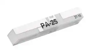
**==> picture [385 x 309] intentionally omitted <==**

**----- Start of picture text -----**<br>
Anam<br>PA.25a<br>Specification<br>Part No. PA.25a<br>Product Name Anam<br>Hexa-Band Cellular SMD Antenna<br>GSM / CDMA / DCS / PCS / WCDMA<br>/UMTS /HSDPA / GPRS / EDGE<br>800 MHz to 2200 MHz<br>Feature High Efficiency Multi-Band SMD Antenna<br>35*5*6mm<br>RoHS Compliant<br>**----- End of picture text -----**<br>


SPE-11-8-061/G   | page 1 of 21

**==> picture [131 x 40] intentionally omitted <==**

## **1. Introduction**

This ceramic multiband cellular antenna uses high grade ceramics which have been developed in Taoglas through years of expertise in delivering the right materials for high performance antennas.

Taoglas designers, through constant research and development have been able to “fit” 6 bands in a small area, while also achieving high efficiency. The PA.25 is a unique SMT solution which is delivered on

tape and reel. For very detailed integration information additional to this specification please download our comprehensive PA.25 integration application note from our website.

## **1.1  Key Advantages**

**1.** Highest efficiency in small size 35*5*6mm. A comparative metal, FR4, FPC, whip, rod, helix antenna would have much more reduced efficiency in this configuration for the same size due to their different dielectric constants.

**2.** More resistant to detuning compared to other antenna integrations. If tuning is required it can be tuned for the device environment. There is no need for new tooling, thereby saving money if customisation is required.

**3.** Highly reliable and robust– its predecessor the PA.22 antenna is used by the world’s leading auto makers in extremely challenging environments. The antenna meets all temperature and mechanical specs required (vibration, drop tests etc)

- **4** . Rectangular shape - Easy to integrate. Other antenna designs come in irregular shapes and sizes making them hard to integrate.

**5.** SMD (On-Board) antenna saves on labor, cable and connector costs, leads to higher integration yield rates, and reduces losses in transmission.

**6.** It can be mounted directly on edge of device main-board.

**7.** Transmission losses are kept to absolute minimum resulting in much improved over the air (OTA) device performance compared to similar efficiency cable and connector antenna solutions

**8.** Reductions in probability of radiated spurious emissions compared to other antenna technologies are observed when using the PA.25 and strictly following this application note layout

**9.** Achieves moderate to high gain in both vertical and horizontal polarization planes.

This feature is very useful in certain wireless communications where the antenna orientation is not fixed and the reflections or multipath signals may be present from any plane.

In those cases the important parameter to be considered is the total field strength, which is the vector sum of the signal from the horizontal and vertical polarization planes at any instant in time.

SPE-11-8-061/G   | page 2 of 21

## **2. Electrical Characteristics**

|**Parameter**|**Specification**|
|---|---|
|**Working Frequency**|824~960MHz to 1700~2170MHz|
|**Dimensions**|35*5*6mm|
|**VSWR**|3:1 max(depends on the special environment)|
|**Polarization**|Linear|
|**Impedance**|50 Ω|
|**Operating Temperature**|-40°C~+105°C|
|**Termination**|Ag (EnvironmentallyFriendlyPb Free)|


- Ground Plane Size 40*97mm

- Actual Electrical value will depend on customer ground plane size.

## **3. Key Antenna Performance Indicators**

Measured in Satimo Starlab system

*Efficiency & Gain (Ground Plane Length: 97 mm)

|*Efficiency & Gain (Ground Plane Length: 97 mm)|*Efficiency & Gain (Ground Plane Length: 97 mm)|*Efficiency & Gain (Ground Plane Length: 97 mm)|*Efficiency & Gain (Ground Plane Length: 97 mm)|*Efficiency & Gain (Ground Plane Length: 97 mm)|*Efficiency & Gain (Ground Plane Length: 97 mm)|||||||
|---|---|---|---|---|---|---|---|---|---|---|---|
|**Hexa-band Antenna PA.25a peak gain parameter Summary**||||||||||||
|**Band**|**GSM(MHz)**||||**3G**|**DCS(MHz)**||**PCS(MHz)**||**WCDMA(MHz)**||
||**824**|**890**|**880**|**960**|**1700**|**1710**|**1880**|**1850**|**1990**|**2110**|**2170**|
|**Peak Gain(dBi)**|1.49|0.92|1.76|1.35|2.40|2.53|2.38|2.30|2.46|2.69|4.62|
|**Efficiency (%)**|60.6|65.4|69.3|64.6|51.0|54.7|63.1|61.6|51.5|56.2|65.8|


SPE-11-8-061/G   | page 3 of 21

## **3.1   Reference efficiency data with different ground plane length**

## **3.2   S11 - Return Loss**

**==> picture [400 x 300] intentionally omitted <==**

**----- Start of picture text -----**<br>
Tr1     S11  Log  Mag 3.000dB/  Ref 0.000dB  [F1]<br>a<br>3.000<br>>1   824.00000 MHz     -6.3905 dB<br>0.000 >2   960.00000 MHz     -12.714 dB<br>>3   1.7100000 GHz     -10.787 dB<br>>4   2.1700000 GHz     -13.510 dB<br>-3.000<br>-6.000<br>1<br>1<br>-9.000<br>-12.00 3 4<br>2<br>-15.00<br>-18.00<br>-21.00<br>-24.00<br>-27.00<br>**----- End of picture text -----**<br>


SPE-11-8-061/G   | page 4 of 21

**==> picture [131 x 40] intentionally omitted <==**

## **3.3   S11 – Smith Chart**

Tr1 S11   Smith   (R+j X)   Scale  1.000U   [F1] 1      824.00000  MHz      32.824 Ω      -41.861 Ω       4.6141 pF 2      960.00000  MHz      51.214 Ω        29.208 Ω       4.8422 nH 3      1.7100000  GHz       31.210 Ω       8.0208 Ω        746.52 pH >4      2.1700000  GHz       36.866 Ω      -11.950 Ω        6.1373 pF ~~2~~ 3 4 1

**==> picture [106 x 106] intentionally omitted <==**

SPE-11-8-061/G   | page 5 of 21

**==> picture [131 x 40] intentionally omitted <==**

## **3.4   VSWR**

**==> picture [468 x 358] intentionally omitted <==**

**----- Start of picture text -----**<br>
Tr1     S11   SWR   1.000/ Ref 1.000<br>11.00<br>>1     824.00000 MHz     3.2646<br>2     890.00000 MHz     2.0309<br>10.00 3     880.00000 MHz     2.0212<br>4     960.00000 MHz     2.5039<br>5     1.7100000 GHz     2.0375<br>6     1.8800000 GHz     1.6615<br>9.000 7     1.9900000 GHz     1.9366<br>8     2.1100000 GHz     1.5498<br>9     2.1700000 GHz     1.5954<br>8.000<br>7.000<br>6.000<br>5.000<br>4.000<br>1 1<br>3.000<br>2.000 4<br>32 5 7<br>6 8 9<br>1.000<br>**----- End of picture text -----**<br>


SPE-11-8-061/G   | page 6 of 21

## **3.5   Radiation Patterns**

SPE-11-8-061/G   | page 7 of 21

## **3.5   Radiation Patterns**

SPE-11-8-061/G   | page 8 of 21

## **3.5   Radiation Patterns**

SPE-11-8-061/G   | page 9 of 21

**==> picture [131 x 40] intentionally omitted <==**

## **3.6   Test data below shows the affect of different ground plane lengths on the antenna in terms of antenna efficiency on all frequencies**

||**9.5cm**|**8.5cm**|**7.5cm**|**6.5cm**|**5.5cm**|**4.5cm**|
|---|---|---|---|---|---|---|
|**800MHz**|51%|33%|24%|18%|11%|10%|
|**815MHz**|57%|38%|27%|20%|12%|10%|
|**830MHz**|63%|44%|33%|24%|14%|13%|
|**845MHz**|70%|51%|39%|29%|17%|15%|
|**860MHz**|70%|53%|42%|32%|20%|17%|
|**875MHz**|71%|57%|45%|35%|22%|19%|
|**890MHz**|65%|53%|42%|33%|20%|17%|
|**905MHz**|65%|53%|43%|33%|19%|16%|
|**920MHz**|66%|55%|46%|36%|22%|19%|
|**935MHz**|68%|57%|48%|38%|23%|20%|
|**950MHz**|60%|50%|42%|34%|22%|19%|
|**965MHz**|67%|55%|46%|38%|24%|21%|
|**980MHz**|65%|54%|45%|37%|23%|20%|
|**995MHz**|63%|51%|43%|34%|22%|19%|
|**1010MHz**|64%|52%|43%|35%|22%|20%|
|**1025MHz**|65%|52%|42%|34%|22%|20%|
|**1040MHz**|57%|45%|37%|29%|18%|16%|
|**1055MHz**|58%|45%|36%|28%|18%|16%|
|**1070MHz**|59%|46%|37%|29%|18%|16%|
|**1085MHz**|54%|43%|34%|26%|16%|14%|
|**1100MHz**|52%|41%|32%|24%|14%|13%|
|**1115MHz**|49%|39%|30%|22%|13%|11%|
|**1130MHz**|43%|35%|27%|20%|11%|10%|
|**1145MHz**|38%|32%|24%|18%|10%|8%|
|**1160MHz**|32%|28%|22%|16%|9%|7%|
|**1175MHz**|28%|25%|20%|14%|8%|7%|
|**1190MHz**|26%|24%|19%|14%|7%|6%|
|**1205MHz**|21%|21%|17%|12%|7%|6%|
|**1220MHz**|14%|15%|12%|9%|5%|4%|
|**1235MHz**|13%|14%|12%|9%|5%|4%|
|**1250MHz**|11%|12%|11%|8%|4%|4%|
|**1265MHz**|10%|11%|10%|8%|4%|4%|


SPE-11-8-061/G   | page 10 of 21

**==> picture [131 x 40] intentionally omitted <==**

## **3.6   Test data below shows the affect of different ground plane lengths on the antenna in terms of antenna efficiency on all frequencies**

|**1280MHz**|8%|9%|9%|7%|4%|3%|
|---|---|---|---|---|---|---|
|**1295MHz**|8%|9%|9%|7%|4%|4%|
|**1310MHz**|6%|7%|7%|6%|4%|3%|
|**1325MHz**|5%|6%|6%|5%|3%|3%|
|**1340MHz**|5%|5%|5%|5%|4%|3%|
|**1355MHz**|5%|5%|5%|5%|4%|4%|
|**1370MHz**|5%|5%|5%|5%|4%|4%|
|**1385MHz**|5%|5%|5%|5%|5%|5%|
|**1400MHz**|5%|5%|5%|5%|5%|5%|
|**1415MHz**|5%|5%|5%|5%|5%|6%|
|**1430MHz**|6%|6%|6%|6%|6%|6%|
|**1445MHz**|6%|6%|7%|7%|6%|6%|
|**1460MHz**|7%|7%|8%|9%|7%|7%|
|**1475MHz**|8%|9%|10%|11%|9%|8%|
|**1490MHz**|9%|11%|12%|14%|11%|10%|
|**1505MHz**|11%|13%|15%|17%|13%|11%|
|**1520MHz**|12%|14%|17%|20%|16%|13%|
|**1535MHz**|13%|15%|18%|21%|18%|15%|
|**1550MHz**|15%|17%|21%|25%|22%|17%|
|**1565MHz**|19%|21%|25%|30%|27%|21%|
|**1580MHz**|22%|24%|28%|34%|33%|25%|
|**1595MHz**|25%|28%|32%|39%|39%|30%|
|**1610MHz**|28%|31%|35%|42%|43%|34%|
|**1625MHz**|31%|34%|38%|46%|48%|38%|
|**1640MHz**|36%|38%|42%|50%|54%|44%|
|**1655MHz**|41%|42%|47%|55%|61%|50%|
|**1670MHz**|45%|47%|51%|59%|66%|56%|
|**1685MHz**|47%|49%|52%|60%|66%|56%|
|**1700MHz**|51%|52%|56%|63%|70%|59%|
|**1715MHz**|57%|58%|63%|70%|76%|65%|
|**1730MHz**|51%|52%|55%|61%|65%|57%|
|**1745MHz**|53%|54%|58%|63%|67%|59%|
|**1760MHz**|61%|62%|67%|72%|74%|65%|
|**1775MHz**|60%|62%|66%|71%|73%|64%|
|**1790MHz**|59%|60%|64%|70%|70%|61%|
|**1805MHz**|63%|65%|71%|77%|75%|65%|
|**1820MHz**|61%|63%|69%|75%|74%|63%|


SPE-11-8-061/G   | page 11 of 21

**==> picture [131 x 40] intentionally omitted <==**

## **3.6   Test data below shows the affect of different ground plane lengths on the antenna in terms of antenna efficiency on all frequencies**

|**1835MHz**|61%|63%|68%|75%|73%|62%|
|---|---|---|---|---|---|---|
|**1850MHz**|62%|65%|70%|77%|75%|64%|
|**1865MHz**|63%|66%|72%|80%|77%|64%|
|**1880MHz**|63%|66%|73%|81%|78%|65%|
|**1895MHz**|62%|65%|72%|80%|78%|65%|
|**1910MHz**|60%|62%|68%|77%|75%|62%|
|**1925MHz**|58%|60%|66%|75%|74%|60%|
|**1940MHz**|56%|58%|64%|72%|73%|59%|
|**1955MHz**|54%|55%|61%|69%|71%|58%|
|**1970MHz**|53%|53%|58%|67%|70%|57%|
|**1985MHz**|52%|51%|56%|64%|69%|56%|
|**2000MHz**|51%|50%|54%|62%|68%|55%|
|**2015MHz**|49%|47%|51%|58%|64%|53%|
|**2030MHz**|50%|48%|51%|59%|66%|54%|
|**2045MHz**|48%|45%|47%|54%|62%|52%|
|**2060MHz**|49%|45%|47%|53%|62%|53%|
|**2075MHz**|53%|48%|49%|56%|67%|57%|
|**2090MHz**|54%|48%|49%|56%|66%|58%|
|**2105MHz**|56%|49%|49%|56%|67%|59%|
|**2120MHz**|58%|50%|50%|56%|68%|61%|
|**2135MHz**|58%|51%|50%|55%|66%|61%|
|**2150MHz**|62%|54%|52%|57%|69%|64%|
|**2165MHz**|66%|57%|55%|59%|72%|68%|
|**2180MHz**|65%|56%|53%|56%|68%|66%|
|**2195MHz**|67%|59%|55%|58%|68%|68%|
|**2210MHz**|67%|60%|56%|57%|66%|66%|
|**2225MHz**|66%|60%|56%|57%|63%|64%|
|**2240MHz**|63%|59%|55%|55%|60%|61%|
|**2255MHz**|62%|59%|56%|55%|58%|59%|
|**2270MHz**|63%|61%|58%|57%|57%|58%|
|**2285MHz**|58%|58%|56%|54%|52%|52%|
|**2300MHz**|58%|59%|58%|57%|51%|52%|


SPE-11-8-061/G   | page 12 of 21

## **4.  Drawings**

## **4.1   Layout for the antenna mounting**

The size of the ground plane for the complete evaluation board is 97x40 mm. The size of the entire board including the antenna area free of ground plane is 107x40 mm. The area occupied by the antenna is 40x13 mm.

SPE-11-8-061/G   | page 13 of 21

## **4.2   Footprint of antenna**

SPE-11-8-061/G   | page 14 of 21

## **4.3   Solder Mask and Solder Areas**

To avoid movements of the antenna in the SMD process, we highly recommend to follow the next solder mask and solder pad areas.

The size of the inductor is 0402. The layout has the area to allocate the inductor with a solder land of 0.6x0.5 m for each pad.

SPE-11-8-061/G   | page 15 of 21

**==> picture [131 x 40] intentionally omitted <==**

## **4.4   Antenna Dimensions**

**==> picture [433 x 486] intentionally omitted <==**

**----- Start of picture text -----**<br>
Bottom<br>Top<br>PA-25<br>XX-YY<br>Week<br>Year<br>Silver<br>Ground Clearance Area<br>XX-YY<br>PA-25<br>**----- End of picture text -----**<br>


**==> picture [92 x 35] intentionally omitted <==**

SPE-11-8-061/G   | page 16 of 21

## **5.  Test Board Dimensions - PAD.25**

The test Board is designed for evaluation purposes with a SMA(F) Connector

The size of the ground plane for the complete evaluation board is 97 x 40 mm. The size of the entire board including the antenna area free of ground plane is 110 x 40 mm. The area occupied by the antenna is 13 x 40 mm.

SPE-11-8-061/G   | page 17 of 21

**==> picture [131 x 40] intentionally omitted <==**

## **5.1** ~~**E**~~ **V** ~~**B Draw**~~ **ing**

**==> picture [402 x 463] intentionally omitted <==**

||**Name**|**Material**|**Finish**|**QTY**|
|---|---|---|---|---|
|~~1~~|~~PA.25.A EVB PCB~~|~~FR4 0.8t~~|~~Black~~|~~1~~|
|~~2~~|~~SMA(F) ST PCB~~|~~Brass~~|~~Gold Plated~~|~~1~~|
|~~3~~|~~PA.25A Antenna~~|~~Ceramics~~|~~White~~|~~1~~|
|4|6.8nH Inductor (0402)|~~Ceram~~i~~cs~~|~~N/A~~|1|


SPE-11-8-061/G   | page 18 of 21

**==> picture [131 x 40] intentionally omitted <==**

## **6.  Transmission Line and Matching Component**

A matching component of a 2nH inductor in parallel with PA.25 is required for the PA.25 to have the optimal performance in the evaluation board, located outside of the ground plane in the space specified in the above drawings.

The matching component in a device we recommend starting with a 2.2 nH for short

ground planes (45-75 mm) and 6.8 nH for larger ground planes (80-100 mm). The inductor is strictly required in the antenna integration (this lumped element is considered as part of the antenna).

Is not possible to determine if further improvement in matching is necessary for a PCB in specific, but we recommend

incorporating in the design extra spaces for a “pi” network in between the GSM module and the edge of the ground plane. The starting point will be putting a 0 ohm resistor in series in the “pi” network (S1) and the required 6.8 nH or 2 nH outside of the ground plane (L1). With these spaces we have 3 options for matching topologies as in the next figures:

**==> picture [331 x 140] intentionally omitted <==**

**----- Start of picture text -----**<br>
S3 S2 L1<br>Antenna<br>S1<br>Module Component<br>Ground Plane Limit<br>Component Component Component<br>**----- End of picture text -----**<br>


**==> picture [103 x 11] intentionally omitted <==**

**----- Start of picture text -----**<br>
“pi” matching network<br>**----- End of picture text -----**<br>


**==> picture [296 x 91] intentionally omitted <==**

**----- Start of picture text -----**<br>
Typical config Typical config Component types<br>S3 S2<br>Inductor<br>S1 S1<br>Capacitor<br>**----- End of picture text -----**<br>


## **“L” and “Inverted-L” matching network**

Further optimization could be done as part of a matching circuit to determine if more components are necessary in the “pi” network, but cannot be determined before, until we test the board with the antenna on it.

SPE-11-8-061/G   | page 19 of 21

**==> picture [131 x 40] intentionally omitted <==**

## **7.  Recommended Reflow Temperature Profile**

The PA.25 can be assembled following either Sn-Pb or Pb-Free assembly processes. The recommended soldering temperatures are as follows:

|**Phase**|**Profle Features**|**Sn-Pb Assembly**|**Pb-Free Assembly**<br>**(SnAgCu)**|
|---|---|---|---|
|Ramp-Up|Avg Ramp-Up Rate<br>(Tsmax to Tp)|3°C/second (max)|3°C/second (max)|
||Temperature Min (Tsmin)|100°C|150°C|
|Preheat|Temperature Max (Tsmax)|150°C|200°C|
||Time (tsmin to tsmax)|60-120 seconds|60-120 seconds|
|Refow|Temperature (TL)<br>Total Time Above TLb(tL)|<br>183°C<br>60-150 seconds|217°C<br>60-150 seconds|
|Peak|Temperature (Tp)<br>Time (tp)|235°C<br>10-30 seconds|260°C<br>20-40 seconds|
|Ramp-Down|Rate|6°C/second (max)|6°C/second (max)|
|Time from 25°C|to peak Temperature|6 minutes max|8 minutes max|


**==> picture [424 x 214] intentionally omitted <==**

**----- Start of picture text -----**<br>
tp<br>Tp Ramp-up Critical Zone TL to Tp<br>TL<br>Tsmax<br>Tsmin<br>ts Preheat<br>Ramp-down<br>25°<br>t 25°C to Peak<br>Temperature<br>**----- End of picture text -----**<br>


Time

Temperature profile – (green area) for the assembly process in reflow ovens

SPE-11-8-061/G   | page 20 of 21

## **8. Packaging**

**1.** Blister tape to IEC 286-3 ’ polyester

**2.** Pieces/tape: 450

Taoglas makes no warranties based on the accuracy or completeness of the contents of this document and reserves the right to make changes to specifications and

product descriptions at any time without notice. Taoglas reserves all rights to this document and the information contained herein.

Reproduction, use or disclosure to third parties without express permission is strictly prohibited. Copyright © Taoglas Ltd.

SPE-11-8-061/G   | page 21 of 21
Updated at June 9, 2026
About Novapart
Novapart is a B2B electronic component broker specialising in stock shortages and cost reduction. We source hard-to-find parts and identify compliant alternatives across a catalogue of 410,000+ components from 500+ manufacturers.
Learn more →Stock Shortage Specialist
When a component is unavailable, discontinued or has an unacceptable lead time, we tap into our network of vetted European and Asian distributors to source what you need — without compromising on quality or traceability.
Request a quote →Compliant Alternatives
We identify pin-to-pin, electrically equivalent substitutes that meet the same certifications (RoHS, AEC-Q100, REACH) as your original specification — validated against datasheets, not just part numbers. Often at a lower cost.
BOM Analysis service →