


P6KE440A
TVS Diode, P6KE Series, Unidirectional, 376 V, 776 V, DO-15, 2 Pins
- Manufacturer: STMICROELECTRONICS
- Product type: TVS Diodes
- Product Range:P6KE4 Series; TVS Polarity:Unidirectional; Reverse Stand-Off Voltage Vrwm:376V; Clamping Voltage Vc Max:776V; Diode Case Style:DO-15; No. of Pins:2Pins; Breakdown Voltage Min:380V; B
- SVHC: No SVHC (25-Jun-2025)
- No. of Pins: 2Pins
- TVS Polarity: Unidirectional
- Product Range: P6KE Series
- Qualification: -
- Diode Mounting: Through Hole
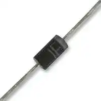
- Diode Case Style: DO-15
- Clamping Voltage Max: 776V
- Reverse Standoff Voltage: 376V
- Maximum Breakdown Voltage: 420V
- Minimum Breakdown Voltage: 380V
- Operating Temperature Max: 175°C
- Peak Pulse Power Dissipation: 600W
| Delivery and price | |
|---|---|
| Units per pack | 500 |
| Price | 0.225 € |
| Current stock | 500+ |
| Lead time | 30 days |
**P6KE**

**==> picture [61 x 39] intentionally omitted <==**

## Transil™, transient voltage surge suppressor (TVS)

**Datasheet** − **production data**

## **Features**

- Peak pulse power: 600 W (10/1000 µs )

- Stand-off voltage range 6.8 to 440 V

- Unidirectional and bidirectional types

- Low clamping factor

- Fast response time

- UL recognized

## **Complies with the following standards**

**==> picture [89 x 89] intentionally omitted <==**

**DO-15 (DO-204AC)**

- IEC 61000-4-2 level 4

   - 15 kV (air discharge)

   - 8 kV (contact discharge)

- MIL STD 883G, method 3015-7 Class 3

   - HBM (human body model)

## **Description**

Transil diodes provide high overvoltage protection by clamping action. Their instantaneous response to transient overvoltages makes them particularly suited to protect voltage sensitive devices such as MOS Technology and low voltage supplied IC’s.

TM:Transil is a trademarks of STMicroelectronics.

1/9

April 2012

Doc ID 3068 Rev 7

This is information on a product in full production.

_www.st.com_

**Characteristics**

**P6KE**

## **1 Characteristics**

## **Table 1. Absolute maximum ratings (Tamb = 25 °C)**

|**Table 1.**|**Absolute maximum ratings (Tamb = 25 °C)**|**Absolute maximum ratings (Tamb = 25 °C)**|||
|---|---|---|---|---|
|**Symbol**|**Parameter**||**Value**|**Unit**|
|PPP|Peak pulse power dissipation(1)|Tj initial= Tamb|600|W|
|P|Power dissipation on infinite heatsink|Tamb= 75 °C|5|W|
|IFSM|Non repetitive surge peak forward current for unidirectional<br>types|tp= 10 ms<br>Tj initial= Tamb|100|A|
|Tstg|Storage temperature range||-65 to + 175|°C|
|Tj|Maximum operating junction temperature||175|°C|
|TL|Maximum lead temperature for soldering during 10 s at 5 mm from case.||260|°C|


1. For a surge greater than the maximum values, the diode will fail in short-circuit.

## **Table 2. Thermal resistances**

**==> picture [461 x 216] intentionally omitted <==**

**----- Start of picture text -----**<br>
Symbol Parameter Value Unit<br>R Junction to leads 20<br>th(j-l)<br>°C/W<br>Rth(j-a) Junction to ambient on printed circuit. L lead = 10 mm 75<br>Figure 1. Electrical characteristics - definitions<br>I I<br>Symbol VRM Parameter Stand-off voltage Unidirectional IF IPP<br>VBR Breakdown voltage<br>VIRMCL Leakage current @ VClamping voltage RM VCLVBR VRM VF V VCLVBR VRM IIRMR V<br>IαPPT Peak pulse currentVoltage temperature coefficient IRMIR IRMIR VRMVBR VCL<br>VF Forward voltage drop<br>RD Dynamic resistance IPP IPP Bidirectional<br>**----- End of picture text -----**<br>


## **Figure 2. Pulse definition for electrical characteristics**

**==> picture [142 x 88] intentionally omitted <==**

**----- Start of picture text -----**<br>
Repetitive pulse current<br>tr = rise time (µs)<br>tp = pulse duration time (µs)<br>tr tp<br>**----- End of picture text -----**<br>


2/9

Doc ID 3068 Rev 7

**Characteristics**

**P6KE**

**Table 3. Electrical characteristics - values (Tamb = 25 °C)**

|**Order code**|**Order code**|**IRM @ VRM**<br>**(1)**<br>**max**|**IRM @ VRM**<br>**(1)**<br>**max**|**VBR @ IR**<br>**(2)**<br>**min**<br>**nom**<br>**max**|**VBR @ IR**<br>**(2)**<br>**min**<br>**nom**<br>**max**|**VBR @ IR**<br>**(2)**<br>**min**<br>**nom**<br>**max**|**VBR @ IR**<br>**(2)**<br>**min**<br>**nom**<br>**max**|**VCL @ IPP**<br>**10/1000 µs**<br>**max**|**VCL @ IPP**<br>**10/1000 µs**<br>**max**|**VCL @ IPP**<br>**8/20µs**<br>**max**|**VCL @ IPP**<br>**8/20µs**<br>**max**|α**T(3)**<br>**max**|**C(4)**<br>**typ**|
|---|---|---|---|---|---|---|---|---|---|---|---|---|---|
|**Unidirectional**|**Bidirectional**|**µA**|**V**|**V**|**V**|**V**|**mA**|**V**|**A**|**V**|**A**|**10-4/ °C**|**pF**|
|P6KE6V8A|P6KE6V8CA|10|5.8|6.45|6.8|7.14|10|10.5|57|13.4|298|5.7|4000|
|P6KE7V5A|P6KE7V5CA|10|6.4|7.13|7.5|7.88|10|11.3|53|14.5|276|6.1|3700|
|P6KE10A|P6KE10CA|1|8.55|9.5|10|10.5|1|14.5|41|18.6|215|7.5|2800|
|P6KE12A|P6KE12CA|0.5|10|11.4|12|12.6|1|16.7|36|21.7|184|7.8|2300|
|P6KE15A|P6KE15CA|0.5|13|14.3|15|15.8|1|21.2|28|27.2|147|8.4|1900|
|P6KE18A|P6KE18CA|0.5|15|17.1|18|18.9|1|25.2|24|32.5|123|8.8|1600|
|P6KE22A|P6KE22CA|0.5|19|20.9|22|23.1|1|30.6|20|39.3|102|9.2|1350|
|P6KE24A|P6KE24CA|0.5|20|22.8|24|25.2|1|33.2|18|42.8|93|9.4|1250|
|P6KE27A|P6KE27CA|0.5|23|25.7|27|28.4|1|37.5|16|48.3|83|9.6|1150|
|P6KE30A|P6KE30CA|0.5|26|28.5|30|31.5|1|41.5|14.5|53.5|75|9.7|1075|
|P6KE33A|P6KE33CA|0.5|28|31.4|33|34.7|1|45.7|13.1|59|68|9.8|1000|
|P6KE36A|P6KE36CA|0.5|31|34.2|36|37.8|1|49.9|12|64.3|62|9.9|950|
|P6KE39A|P6KE39CA|0.5|33|37.1|39|41.0|1|53.9|11.1|69.7|57|10.0|900|
|P6KE47A|P6KE47CA|0.5|40|44.7|47|49.4|1|64.8|9.3|84|48|10.1|800|
|P6KE56A|P6KE56CA|0.5|48|53.2|56|58.8|1|77|7.8|100|40|10.3|700|
|P6KE68A|P6KE68CA|0.5|58|64.6|68|71.4|1|92|6.5|121|33|10.4|625|
|P6KE82A|P6KE82CA|0.5|70|77.9|82|86.1|1|113|5.3|146|27|10.5|550|
|P6KE100A|P6KE100CA|0.5|85|95.0|100|105|1|137|4.4|178|22.5|10.6|500|
|P6KE120A|P6KE120CA|0.5|102|114|120|126|1|165|3.6|212|19|10.7|450|
|P6KE150A|P6KE150CA|0.5|128|143|150|158|1|207|2.9|265|15|10.8|400|
|P6KE180A|P6KE180CA|0.5|154|171|180|189|1|246|2.4|317|12.6|10.8|360|
|P6KE200A|P6KE200CA|0.5|171|190|200|210|1|274|2.2|353|11.3|10.8|350|
|P6KE220A|P6KE220CA|0.5|188|209|220|231|1|328|1.85|388|10.3|10.8|330|
|P6KE250A|P6KE250CA|0.5|213|237|250|263|1|344|1.75|442|9|11|310|
|P6KE300A|P6KE300CA|0.5|256|285|300|315|1|414|1.45|529|7.6|11|290|
|P6KE350A|P6KE350CA|0.5|299|332|350|368|1|482|1.25|618|6.5|11|270|
|P6KE400A|P6KE400CA|0.5|342|380|400|420|1|548|1.1|706|5.7|11|360|
|P6KE440A|P6KE440CA|0.5|376|418|440|462|1|603|1.0|776|5.2|11|350|


1. For bidirectional types having VRM ≤ 10V, IRM is multiplied by 2

2. Pulse test: t < 50 ms. p

3. ΔVBR = αT * (Tamb - 25) * VBR(25°C).

4. VR = 0 V,  F = 1 MHz. For bidirectional types, capacitance value is divided by 2.

3/9

Doc ID 3068 Rev 7

**Characteristics**

**P6KE**

**Figure 3. Peak power dissipation vs. initial Figure 4. Peak pulse power vs. exponential junction temperature pulse duration. (printed circuit board)**

**==> picture [462 x 343] intentionally omitted <==**

**----- Start of picture text -----**<br>
% Ppp (W)<br>100<br>80<br>60<br>40<br>20<br>Tj initial (°C)ø<br>0<br>0 20 40 60 80 100 120 140 160 180 200 0.001 0.01 0.1 1 10 100<br>Figure 5. Clamping voltage vs. peak pulse  Figure 6. Capacitance vs. reverse applied<br>current [(1)] voltage for unidirectional types<br>(typical values).<br>1000 VCL (V) C (pF)<br>P6KE 440A % Ipp Tj initial = 25øC° 10000<br>P6KE 220A 100 50 F=Tj =1 25MHz°øC<br>100 P6KE P6KE 68A 100A 0 tr tp t r < 10 s t 1000<br>P6KE 39A<br>P6KE 22A<br>P6KE 12A<br>10 P6KE 6V8A 100<br>Exponential waveform: tp = 20µs<br>tt p p = 1ms= 10ms Ipp (A) V R (V)<br>1 10<br>0.1 1 10 100 1000 1 10 100 500<br>P6KE6V8A<br>P6KE 15A<br>P6KE68A<br>P6KE200A<br>**----- End of picture text -----**<br>


1. The curves in _Figure 5_ are specified for a junction temperature of 25°C  before surge. The given results may be extrapolated for other junction temperatures by using the following formula : ΔVBR = αT x [Tamb -25] x VBR(25°C) For intermediate voltages, extrapolate the given results.

**Figure 7. Capacitance vs. reverse applied voltage for bidirectional types (typical values).**

**Figure 8. Peak forward voltage drop vs. peak forward current for unidirectional types (typical value).[(1)]**

**==> picture [462 x 164] intentionally omitted <==**

**----- Start of picture text -----**<br>
C (pF)<br>10000<br>Tj = 25°øC<br>F= 1 MHz<br>1000<br>100<br>V R (V)<br>10<br>1 10 100 500<br>1. Multiply by 2 for units with VBR > 220 V.<br>P6KE 15CA<br>P6KE68CA<br>P6KE6V8CA<br>P6KE200CA<br>**----- End of picture text -----**<br>


4/9

Doc ID 3068 Rev 7

**Characteristics**

**P6KE**

**Figure 9. Transient thermal impedance Figure 10. Relative variation of leakage junction to ambient vs. pulse current vs. junction temperature duration**

**==> picture [196 x 140] intentionally omitted <==**

**----- Start of picture text -----**<br>
Zth (j-a) (°C/W)<br>100<br>Printed circuit board FR4,<br>L lead  = 10 mm<br>10<br>tp<br>1<br>0.01 0.1 1 10 100 1000<br>**----- End of picture text -----**<br>


**==> picture [220 x 140] intentionally omitted <==**

5/9

Doc ID 3068 Rev 7

**Ordering information scheme**

**P6KE**

## **2 Ordering information scheme**

## **Figure 11. Ordering information scheme**

**==> picture [226 x 133] intentionally omitted <==**

**----- Start of picture text -----**<br>
P6   KE   100   CA   RL<br>Peak Pulse Power<br>P6 = 600 W<br>Breakdown Voltage<br>100 = 100 V<br>Types<br>A = Unidirectional<br>CA = Bidirectional<br>Packaging<br>Blank = Ammopack tape<br>RL = Tape and reel<br>**----- End of picture text -----**<br>


## **3 Package information**

- Epoxy meets UL94, V0

- Lead-free package

In order to meet environmental requirements, ST offers these devices in different grades of ECOPACK[®] packages, depending on their level of environmental compliance. ECOPACK[®] specifications, grade definitions and product status are available at: _www.st.com_ . ECOPACK[®] is an ST trademark.

## **Table 4. DO-15 dimensions**

||||||**C**|**Ref.**|**Dimensions**|**Dimensions**|**Dimensions**|**Dimensions**|
|---|---|---|---|---|---|---|---|---|---|---|
||||||||**Millimeters**||**Inches**||
||**C**||**A**||**C**||||||
||||||||||||
||||||||**Min.**|**Max.**|**Min.**|**Max.**|
|||||||A|6.05|6.75|0.238|0.266|
||||||||||||
||**D**|||||B|2.95|3.53|0.116|0.139|
|||||**B**|||||||
|||||||C|26|31|1.024|1.220|
||||||||||||
|||||||D|0.71|0.88|0.028|0.035|


6/9

Doc ID 3068 Rev 7

**Package information**

**P6KE**

**Table 5.**

**Marking**

|**Table 5.**<br>**Marking**||||
|---|---|---|---|
|**Unidirectional**<br>**order code**|**Marking(1)**|**Bidirectional**<br>**order code**|**Marking(1)**|
|P6KE6V8A|P6KE6V8A|P6KE6V8CA|P6KE6V8CA|
|P6KE7V5A|P6KE7V5A|P6KE7V5CA|P6KE7V5CA|
|P6KE10A|P6KE10A|P6KE10CA|P6KE10CA|
|P6KE12A|P6KE12A|P6KE12CA|P6KE12CA|
|P6KE15A|P6KE15A|P6KE15CA|P6KE15CA|
|P6KE18A|P6KE18A|P6KE18CA|P6KE18CA|
|P6KE22A|P6KE22A|P6KE22CA|P6KE22CA|
|P6KE24A|P6KE24A|P6KE24CA|P6KE24CA|
|P6KE27A|P6KE27A|P6KE27CA|P6KE27CA|
|P6KE30A|P6KE30A|P6KE30CA|P6KE30CA|
|P6KE33A|P6KE33A|P6KE33CA|P6KE33CA|
|P6KE36A|P6KE36A|P6KE36CA|P6KE36CA|
|P6KE39A|P6KE39A|P6KE39CA|P6KE39CA|
|P6KE47A|P6KE47A|P6KE47CA|P6KE47CA|
|P6KE56A|P6KE56A|P6KE56CA|P6KE56CA|
|P6KE68A|P6KE68A|P6KE68CA|P6KE68CA|
|P6KE82A|P6KE82A|P6KE82CA|P6KE82CA|
|P6KE100A|P6KE100A|P6KE100CA|P6KE100CA|
|P6KE120A|P6KE120A|P6KE120CA|P6KE120CA|
|P6KE150A|P6KE150A|P6KE150CA|P6KE150CA(2)|
|P6KE180A|P6KE180A|P6KE180CA|P6KE180CA|
|P6KE200A|P6KE200A|P6KE200CA|P6KE200CA|
|P6KE220A|P6KE220A|P6KE220CA|P6KE220CA|
|P6KE250A|P6KE250A|P6KE250CA|P6KE250CA|
|P6KE300A|P6KE300A|P6KE300CA|P6KE300CA|
|P6KE350A|P6KE350A|P6KE350CA|P6KE350CA|
|P6KE400A|P6KE400A(2)|P6KE400CA|P6KE400CA|
|P6KE440A|P6KE440A(2)|P6KE440CA|P6KE440CA|


1. Includes a space character after P6KE for ECOPACK2 compliant devices

2. Includes a space character after P6KE for ECOPACK1 compliant devices in tape and reel packaging.

7/9

Doc ID 3068 Rev 7

**Ordering information**

**P6KE**

## **4 Ordering information**

## **Table 6. Ordering information**

|**Order code**|**Marking(1)**|**Package**|**Weight**|**Base qty**|**Delivery mode**|
|---|---|---|---|---|---|
|P6KExxxx|See_Table 5_|DO-15|0.4 g|1000|Ammopack|
|P6KExxxxRL||||6000|Tape and reel|


1. Logo, date code, type code, cathode band (for unidirectional types only).

## **5 Revision history**

**Table 7. Document revision history**

|**Date**|**Revision**|**Changes**|
|---|---|---|
|Feb-2003|4A|Last update|
|Oct-2004|5|1/ Note 5, figure 7 on page 4, updated from VBR> 220V to<br>VBR ≥200V.<br>2/ Types table on page 2: IPP(@10/1000µs) changed for<br>P6KE220xx to P6KE440xx|
|14-Sep-2011|6|Updated IRM@ VRMvalues, VBRmax@ IRfor P6KE33 and<br>order codes in_Table 3_. Updated footnotes to_Table 5_.<br>Updated TLtemperature in_Table 1._|
|26-Apr-2012|7|Corrected typographical area_Table 3_.|


8/9

Doc ID 3068 Rev 7

**P6KE**

## **Please Read Carefully:**

Information in this document is provided solely in connection with ST products. STMicroelectronics NV and its subsidiaries (“ST”) reserve the right to make changes, corrections, modifications or improvements, to this document, and the products and services described herein at any time, without notice.

All ST products are sold pursuant to ST’s terms and conditions of sale.

Purchasers are solely responsible for the choice, selection and use of the ST products and services described herein, and ST assumes no liability whatsoever relating to the choice, selection or use of the ST products and services described herein.

No license, express or implied, by estoppel or otherwise, to any intellectual property rights is granted under this document. If any part of this document refers to any third party products or services it shall not be deemed a license grant by ST for the use of such third party products or services, or any intellectual property contained therein or considered as a warranty covering the use in any manner whatsoever of such third party products or services or any intellectual property contained therein.

**UNLESS OTHERWISE SET FORTH IN ST’S TERMS AND CONDITIONS OF SALE ST DISCLAIMS ANY EXPRESS OR IMPLIED WARRANTY WITH RESPECT TO THE USE AND/OR SALE OF ST PRODUCTS INCLUDING WITHOUT LIMITATION IMPLIED WARRANTIES OF MERCHANTABILITY, FITNESS FOR A PARTICULAR PURPOSE (AND THEIR EQUIVALENTS UNDER THE LAWS OF ANY JURISDICTION), OR INFRINGEMENT OF ANY PATENT, COPYRIGHT OR OTHER INTELLECTUAL PROPERTY RIGHT.**

**UNLESS EXPRESSLY APPROVED IN WRITING BY TWO AUTHORIZED ST REPRESENTATIVES, ST PRODUCTS ARE NOT RECOMMENDED, AUTHORIZED OR WARRANTED FOR USE IN MILITARY, AIR CRAFT, SPACE, LIFE SAVING, OR LIFE SUSTAINING APPLICATIONS, NOR IN PRODUCTS OR SYSTEMS WHERE FAILURE OR MALFUNCTION MAY RESULT IN PERSONAL INJURY, DEATH, OR SEVERE PROPERTY OR ENVIRONMENTAL DAMAGE. ST PRODUCTS WHICH ARE NOT SPECIFIED AS "AUTOMOTIVE GRADE" MAY ONLY BE USED IN AUTOMOTIVE APPLICATIONS AT USER’S OWN RISK.**

Resale of ST products with provisions different from the statements and/or technical features set forth in this document shall immediately void any warranty granted by ST for the ST product or service described herein and shall not create or extend in any manner whatsoever, any liability of ST.

ST and the ST logo are trademarks or registered trademarks of ST in various countries.

Information in this document supersedes and replaces all information previously supplied.

The ST logo is a registered trademark of STMicroelectronics. All other names are the property of their respective owners.

© 2012 STMicroelectronics - All rights reserved

## STMicroelectronics group of companies

Australia - Belgium - Brazil - Canada - China - Czech Republic - Finland - France - Germany - Hong Kong - India - Israel - Italy - Japan - Malaysia - Malta - Morocco - Philippines - Singapore - Spain - Sweden - Switzerland - United Kingdom - United States of America

**www.st.com**

9/9

Doc ID 3068 Rev 7
Updated at June 5, 2026
STMicroelectronics is a global leader in the semiconductor industry, recognized for developing highly integrated, energy-efficient solutions that power modern electronics. With a strong focus on innovation, ST provides a comprehensive portfolio of microelectronics that address the demanding requirements of industrial, automotive, communications, and consumer applications. Our extensive selection of STMicroelectronics components is built around a robust lineup of discrete semiconductors and circuit protection devices. We offer a wide variety of single MOSFETs, Schottky diodes, and fast and ultrafast recovery rectifier diodes, designed to deliver exceptional efficiency and thermal performance in power management and conversion systems. For robust circuit protection, our inventory features hundreds of transient voltage suppressors and TVS diodes that safeguard sensitive electronic components against destructive voltage spikes. In addition to core power discretes like TRIACs, SCRs, bipolar transistors, and single IGBTs, our STMicroelectronics range includes specialized integrated passive filters and MEMS sensors. Furthermore, ST offers advanced integrated passive devices, such as baluns and RF filters, which utilize high-quality monolithic RF IPD processes on glass or high-resistance silicon substrates. These components provide competitive cost structures, reduced power losses, and simplified RFIC-to-antenna matching, ensuring optimal system performance and delivering the reliability required for next-generation wireless and power designs.
About Novapart
Novapart is a B2B electronic component broker specialising in stock shortages and cost reduction. We source hard-to-find parts and identify compliant alternatives across a catalogue of 540,000+ components from 500+ manufacturers.
Learn more →Stock Shortage Specialist
When a component is unavailable, discontinued or has an unacceptable lead time, we tap into our network of vetted European and Asian distributors to source what you need — without compromising on quality or traceability.
Request a quote →Compliant Alternatives
We identify pin-to-pin, electrically equivalent substitutes that meet the same certifications (RoHS, AEC-Q100, REACH) as your original specification — validated against datasheets, not just part numbers. Often at a lower cost.
BOM Analysis service →