
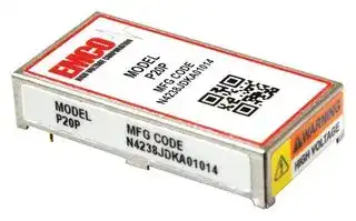


P12N
High Voltage DC/DC Converter, Regulated, Negative Output, Fixed, Adjustable, 2.4 mW, 2 µA
- Manufacturer: XP POWER
- Product type:
- Product Range:P Series; Output Power Max:2.4mW; Output Voltage Min:0V; Output Voltage Max:-1.2kV; Output Current Max:2µA; Polarity:Negative Output; DC / DC Converter Output Type:Fixed
- SVHC: No SVHC (15-Jan-2018)
- Depth: 35.05mm
- Width: 17.27mm
- Height: 6.2mm
- Polarity: Negative Output
- Power Rating: 2.4mW
- Product Range: P Series
- Output Power Max: 2.4mW
- Output Current Max: 2µA
- Output Voltage Max: -1.2kV
- Output Voltage Min: 0V
- Input Voltage DC Max: 12V
- Input Voltage DC Min: 5V
- Power Supply Mounting: Through Hole
- DC / DC Converter Type: DIP
- DC / DC Converter Output Type: Fixed, Adjustable
- High Voltage Power Supply Type: Regulated
| Delivery and price | |
|---|---|
| Units per pack | 5 |
| Price | 259.52 € |
| Current stock | 10+ |
| Lead time | 30 days |
## P Series

## 2.4mW

## DC-HVDC CONVERTER

The P Series of micro-power DC to high voltage DC converters feature extremely low ripple (<100μV) and low EMI/RFI due to a unique magnetic free design. Fully regulated and programmable outputs of 0 to 1200 volts or 0 to 2000 volts are available in positive or negative polarity. A precision on-board voltage reference allows for simple configuration for full scale, fixed or variable output. A high impedance voltage programming input allow for easy system integration. Voltage monitoring is provided at a 1000:1 ratio.

Very low power consumption and light weight, with a case height of less than 0.220 inches, make these PCB mount modules ideal for portable, battery powered equipment. Soft-start high voltage ramp-rates are designed in to further protect sensitive detectors to support long-term reliability.

## **Features** [i • Precision Voltage Regulated

• Output Voltages 1.2kV and 2kV

- Ultra-Low Noise, Magnetic Free Design

- Soft-Start for Sensitive Detectors

- Low Ripple, <100μV

## **Typical Applicati** ~~**on**~~ **s**

2) ~~@~~

   - Portable Toxin Detection

   - Electrostatic Applications

   - Low Power Biasing

   - Piezo Devices

   - Battery Po ~~were~~ d Eq ~~uipm~~ ent

- Output Voltage Monitor

## **Dimensions**

- On-board Voltage Reference

- Standard and Extended Operating Temperatures

1.38” x 0.68” x 0.25” (35.1 x 17.3 x 6.40mm)

- Lightweight Shielded Case

- 3 Year Warranty

## **Models & Ratings**

|Model Number<br>P12N|Output Voltage<br>0 to -1200V|Output Current<br>2μA|
|---|---|---|
|P12P|0 to +1200V|2μA|
|P12P-T|0 to +1200V|2μA|
|P20N|0 to -2000V|1μA|
|P20P|0 to +2000V|1μA|
|P20P-T|0 to +2000V|1μA|


DC-HVDC CONVERTER

## P Series

## **Input**

|12Vin Models|12Vin Models|12Vin Models|12Vin Models|12Vin Models|12Vin Models|
|---|---|---|---|---|---|
|Characteristc|Minimum|Typical|Maximum|Units|Notes & Conditons|
|Input Voltage Range|5||12.0|VDC|Input voltage range is 6V to 12V below -10°C|
|Input Current, No Load|||2.1, 2.6|mA|For 1.2kV, 2kVout, @5V input|
|Input Current, No Load|||3.3, 3.6|mA|For 1.2kV, 2kVout, @5V input|
|Input Current, Capacitance||1||μF||
|Control Voltage, VCTL|0||+4.096|VDC||


## **Output**

**==> picture [540 x 23] intentionally omitted <==**

**----- Start of picture text -----**<br>
Characteristic Minimum Typical Maximum Units Notes & Conditions<br>**----- End of picture text -----**<br>


|Characteristc|Minimum|Typical|Maximum|Units|Notes & Conditons|
|---|---|---|---|---|---|
|Output Programming|||100|%||
|Output Voltage Tolerance||±1||%|For Max Vout|
|Standby Current|||300|μA||
|Minimum Load|No minimum load required|||||
|Ripple and Noise|||100|μV||
|Temperature Coeffcient||250||ppm/°C|With Voltage Reference Output tied to Voltage Control|
|Stability|||100|ppm/hr||
|Voltage Monitor Output||1000:1||Ratio|VMON= VHV/1000|
|Voltage Reference Output||+4.096||VDC|Fixed output voltage|
|Start Up Time||10,15||sec|For 1.2kV, 2kVout, time to output high voltage after applying<br>input|
|Response Time||900||msec|Response to Control Voltage, after Start Up Time|


## **General**

**==> picture [539 x 20] intentionally omitted <==**

**----- Start of picture text -----**<br>
Characteristic Minimum Typical Maximum Units Notes & Conditions<br>**----- End of picture text -----**<br>


|Characteristc|Minimum<br>Typical<br>Maximum<br>Units<br>Notes & Conditons|Minimum<br>Typical<br>Maximum<br>Units<br>Notes & Conditons|Minimum<br>Typical<br>Maximum<br>Units<br>Notes & Conditons|Minimum<br>Typical<br>Maximum<br>Units<br>Notes & Conditons|Minimum<br>Typical<br>Maximum<br>Units<br>Notes & Conditons|
|---|---|---|---|---|---|
|Isolation|N/A – Input ground is connected to output ground|||||
|Construction|Magnet free design, grounded metal case|||||
|Switching Frequency|21.6|24|26.4|kHz||
|Mean Time Between Failure|1.6|||Mhrs|Per Bellcore TR 332 GB +25°C|


Notes:

1. Maximum rated output current is available at maximum rated output voltage.

2

DC-HVDC CONVERTER

## P Series

## **Environmental**

**==> picture [539 x 21] intentionally omitted <==**

**----- Start of picture text -----**<br>
Characteristic Minimum Typical Maximum Units Notes & Conditions<br>**----- End of picture text -----**<br>


|Characteristc|Minimum|Typical|Maximum|Units|Notes & Conditons|
|---|---|---|---|---|---|
|Operating Temperature|-10||+70|°C|Standard operating temperature|
|Storage Temperature|-40||+85|°C|Extended operating temperature, -T suffx|
|Cooling|Natural convection|||||
|Humidity|-55||+105|%RH||


## **Mechanical Details**

**==> picture [525 x 384] intentionally omitted <==**

**----- Start of picture text -----**<br>
TOP  VIEW<br>1.38 (35.1) 0.11<br>(2.8)<br>RECOMMENDED<br>    PCB  LAYOUT HOLE & PAD SIZE:<br>COMPONENT SIDE Ø 0.035         (0.89) &+0.005-0.000<br>0.68  Ø 0.055 (1.40)<br>(17.3) TOP VIEW  7 PLACES<br>1 6<br>Ø 0.025 (.64)  2<br>7 PINS 0.14  3 4 EQ SP @ 0.100 (2.54)<br>(3.6) 4 7 = 0.400 (10.16)<br>0.25 (6.4) 5<br>0.09<br>1.100 (27.94)<br>(2.3)<br>5<br>4 7<br>4 EQ SP @ 0.100 (2.54)<br>3<br>= 0.400 (10.16)<br>2<br>6<br>0.14 (3.6) 1<br>0.09 (2.3) 1.100 (27.94)<br>BOTTOM  VIEW Pin Function Description<br>1 GND Signal Ground<br>2 VIN Input Voltage<br>3 VREF Reference Voltage Output<br>4 VCTL Control Voltage Input<br>5 VMON Voltage Monitor Output<br>6 HV RTN HV Output Return<br>7 HV OUT High Voltage Output<br>HIGH<br>VOLTAGE<br>**----- End of picture text -----**<br>


Notes:

1. All dimensions are in inches (mm)

2. Weight: 0.26oz (7.5g)

3. Tolerance: X.XX±0.02 (0.51)

4. Pin Tolerance: ±0.005 (0.127)

5. All grounds are internally connected to case. Grounded case assists low noise design efforts. Both grounds must be connected to ground for proper operation.

6. Voltage Reference and Voltage Monitor should be left floating when not in use to reduce power consumption.

Specifications subject to change without notice.

3

DC-HVDC CONVERTER

**==> picture [468 x 348] intentionally omitted <==**

**----- Start of picture text -----**<br>
P Series<br>Block Diagram<br>+5V to 12V<br>VOLTAGE REGULATOR HV MULTIPLIER FILTER HV OUT<br>GROUND<br>OSCILLATOR<br>REF VOLTAGE REFERENCE<br>MON<br>HV RETURN<br>FEEDBACK/<br>CONTROL<br>CTL<br>pol<br>Connection Diagram<br>Fixed output (full-scale voltage) Fixed output (reduced voltage)<br>**----- End of picture text -----**<br>


**==> picture [463 x 262] intentionally omitted <==**

**----- Start of picture text -----**<br>
+5 to 12V<br>+5 to 12V<br>GND GND<br>GND GND<br>GND GND IN<br>GND IN GND REF Vhv = Vfs * R2/(R1+R2)<br>REF R1 CTL HV<br>CTL HV Vhv = Vfs MON<br>MON<br>R2<br>4<br>* R1 + R2 ~ 50k<br>GND<br>+ ft<br>Variable output Voltage-controlled output<br>+5 to 12V +5 to 12V<br>GND GND GND GND<br>GND GND GND GND<br>IN IN<br>REF REF<br>R CTL HV Vhv = 0 to Vfs Vctl CTL HV Vhv = Vfs<br>MON MON<br>e e<br>**----- End of picture text -----**<br>


GND * R ~50k

4

25 May 2022
Updated at April 22, 2026
XP Power is a globally recognized leader in the design and manufacture of critical power solutions for the electronics industry. With a steadfast commitment to total quality and in-house engineering expertise, the company delivers highly reliable components that support complex applications across the industrial, healthcare, and technology sectors. Their extensive manufacturing capabilities provide engineers with a broad and dependable source for innovative power products. Our extensive portfolio of XP Power components is heavily focused on robust power and line protection. The core of this offering features a vast selection of high-performance AC/DC converters, designed to meet the rigorous efficiency and footprint demands of modern electronic systems. Complementing these are numerous reliable DC/DC converters, providing versatile options for precise voltage regulation and seamless system integration. Beyond their primary power conversion ranges, XP Power manufactures specialized components to address specific design challenges. Our selection includes essential passive components, such as power line filters for effective EMC and RFI suppression, ensuring signal integrity and strict regulatory compliance. Additionally, we provide dedicated AC/DC LED power supplies tailored for reliable, long-lasting performance in advanced commercial and industrial lighting applications.
About Novapart
Novapart is a B2B electronic component broker specialising in stock shortages and cost reduction. We source hard-to-find parts and identify compliant alternatives across a catalogue of 410,000+ components from 500+ manufacturers.
Learn more →Stock Shortage Specialist
When a component is unavailable, discontinued or has an unacceptable lead time, we tap into our network of vetted European and Asian distributors to source what you need — without compromising on quality or traceability.
Request a quote →Compliant Alternatives
We identify pin-to-pin, electrically equivalent substitutes that meet the same certifications (RoHS, AEC-Q100, REACH) as your original specification — validated against datasheets, not just part numbers. Often at a lower cost.
BOM Analysis service →