
Image not available
Illustrative purposes only

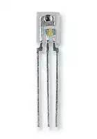
OPL551
Optical Sensor, OPL551 Series, Photologic®, Totem Pole, 4.5 V to 5.5 V
⚠️ Reference pricing provided. In case of supply shortages, we will connect you with our trusted procurement partners to ensure your project's continuity.
- Manufacturer: TT ELECTRONICS / OPTEK TECHNOLOGY
- Product type: Optical / Slot Photoelectric Sensors
- Product Range: OPL551 Series
- Sensor Output: Totem Pole
- Output Current: 16mA
- Supply Voltage DC Max: 5.5V
- Supply Voltage DC Min: 4.5V
| Delivery and price | |
|---|---|
| Units per pack | 100 |
| Price | 1.08 € |
| Current stock | 500+ |
| Lead time | 7 days |
Datasheet

Photologic® Sensor OPL530, OPL531, OPL535, OPL536, OPL550, OPL551, OPL560, OPL561, OPL562, OPL563

## **Features:**

- Choice of four output options in low-cost side-looking package

- Choice of two sensitivity options (OPL560/561/562/563)

- High noise immunity

- Direct TTL/LSTTL CMOS interface

- Data rates to 250 kBaud for all except OPL560 series (200 kBaud)

- Low power consumption

**==> picture [24 x 6] intentionally omitted <==**

**----- Start of picture text -----**<br>
RoHS<br>**----- End of picture text -----**<br>


**Description:** All components in this series include a photodiode, amplifier, voltage regulator, Schmitt trigger and NPN output transistor on a single silicon chip. **OPL560** chips also include a voltage regulator on the chip.  All devices in the series have a  Photologic® chip that is encapsulated in a molded plastic side-looking package with an integral lens (recessed integral lens for OPL535 and OPL536).  This packaging provides enhanced optical coupling, combined with mechanical protection.  The hysteresis characteristics of the Schmitt trigger on each device offers high immunity to noise on input and VCC.

**OPL530** , **OPL531** , **OPL535** and **OPL536** include a 10 K Ω pull-up resistor (RL) from output to VCC.  These components exhibit very stable performance over supply voltages ranging from 4.5 V to 16 V and a wide range of irradiance levels. **OPL550** and **OPL551** devices feature TTL/LSTTL compatible logic level output which can drive up to 8 TTL loads without additional circuitry and medium-speed data rates to 250 kBaud, with typical rise and fall times of 25 nanoseconds. **OPL560** , **OPL561** , **OPL562** and **OPL563** devices feature TTL/LSTTL compatible logic level output which can drive up to 10 TTL loads over supply voltages ranging from 4.5 V to 16 V.

**OPL530** , **OPL531** , **OPL550** , **OPL551** , **OPL560** , **OPL561** , **OPL562** and **OPL563** are mechanically and spectrally matched to  OP140 and OP240 LEDs. **OPL535** and **OPL536** are mechanically and spectrally matched to OP145 and OP245 series LEDs.

**Applications:** Non-contact reflective object sensor, Assembly line automation, Machine automation, Machine safety, End of travel sensor, Door sensor

|**Base Part Number**|**Package**|**Output Type - with Light**|**Input Power Range**<br>**(mW/cm2) [Min/Max]**|**Input Power Range**<br>**(mW/cm2) [Min/Max]**|**Input Power Range**<br>**(mW/cm2) [Min/Max]**|
|---|---|---|---|---|---|
||||**-**|**A**|**B**|
|**OPL530, OPL530-OC**|External Lens|Internal 10K  - High|0.08/0.40|0.08/0.25|0.20/0.40|
|**OPL531A, OPL531-OCA**||Internal 10K  - Low||||
|**OPL535A, OPL535B**|Recessed<br>Lens|Internal 10K  - High||||
|**OPL536A, OPL536-OC, OPL536-OCA**||Internal 10K  - Low||||
|**OPL550, OPL550A, OPL550-OC, OPL550-OCA**|External Lens|Totem Pole - High|0.25/2.4|0.25/1.4|N/A|
|**OPL551A, OPL551-OC, OPL551-OCA**||Totem Pole - Low|0.25/2.5|0.25/1.5||
|**OPL560, OPL560A, OPL560-OCA**||Totem Pole - High|0.09/0.55|0.09/0.36|N/A|
|**OPL561, OPL561-OC, OPL561-OCA**||Totem Pole - Low||||
|**OPL562, OPL562A, OPL562-OC, OPL562-OCA**||Totem Pole - High|0.025/0.23|0.025/0.14  N/A|0.025/0.14  N/A|
|**OPL563, OPL563-OC, OPL563-OCA**||Totem Pole - Low||||
|**OC = Open Collector Output**||||||


## General Note

OPTEK Technology, Inc. 1645 Wallace Drive, Carrollton, TX 75006|Ph: +1 972 323 2200 www.optekinc.com | www.ttelectronics.com

TT Electronics reserves the right to make changes in product specification without notice or liability.  All information is subject to TT Electronics’ own data and is considered accurate at time of going to print.

Issue D      04/2018     Page 1

© TT electronics plc

OPL530, OPL531, OPL535, OPL536, OPL550, 9 OPL551, OPL560, OPL561, OPL562, OPL563

## **OPL530, OPL550, OPL560 Series**

**==> picture [115 x 13] intentionally omitted <==**

**----- Start of picture text -----**<br>
[ MILLIMETERS]<br>DIMENSIONS ARE IN:  INCHES<br>**----- End of picture text -----**<br>


|**Pin #**|**Sensor**|
|---|---|
|1|Ground|
|2|Output|
|3|VCC|


## **OPL535, OPL536 Series**

**==> picture [115 x 12] intentionally omitted <==**

**----- Start of picture text -----**<br>
[ MILLIMETERS]<br>DIMENSIONS ARE IN:  INCHES<br>**----- End of picture text -----**<br>


|**Pin #**|**Sensor**|
|---|---|
|1|Ground|
|2|Output|
|3|VCC|


OPTEK Technology, Inc. 1645 Wallace Drive, Carrollton, TX 75006|Ph: +1 972 323 2200 www.optekinc.com | www.ttelectronics.com

General Note TT Electronics reserves the right to make changes in product specification without notice or liability.  All information is subject to TT Electronics’ own data and is considered accurate at time of going to print.

Issue CD     04/2018     Page 2

© TT electronics plc

OPL530, OPL531, OPL535, OPL536, OPL550, OPL551, OPL560, OPL561, OPL562, OPL563

## **OPL530, OPL531, OPL535, OPL536, OPL550, OPL551, OPL560, OPL561, OPL562, OPL563 (-OC, -OCA, -OCB) OPL550, OPL550A, OPL551A, OPL560, OPL560A, OPL561, OPL562, OPL562A, OPL563, OPL563A**

**==> picture [506 x 254] intentionally omitted <==**

**----- Start of picture text -----**<br>
OPL550/550A/560/560A/562/562A  Totem-Pole  OPL530/535/550/560/562 (-OC, -OCA, -OCB)  Open-Collector<br>VCC O VCC<br>S<br>OUT<br>OUT<br>Me ; GND  rr> + GND<br>2 O<br>OPL 551A/561/563/563A  Inverted Totem-Pole  OPL 531/536/551/561/563 (-OC, -OCA, -OCB)  Inverted Open-Collector<br>VCC VCC<br>OUT<br>-<br>[ J ©) | O<br>Me [> OUT  ne i><br>S<br>GND  GND<br>**----- End of picture text -----**<br>


General Note TT Electronics reserves the right to make changes in product specification without notice or liability.  All information is subject to TT Electronics’ own data and is considered accurate at time of going to print.

OPTEK Technology, Inc. 1645 Wallace Drive, Carrollton, TX 75006|Ph: +1 972 323 2200 www.optekinc.com | www.ttelectronics.com

Issue CD     04/2018     Page 3

© TT electronics plc

OPL530, OPL531, OPL535, OPL536, OPL550, OPL551, OPL560, OPL561, OPL562, OPL563

## **OPL530, OPL531A, OPL535A, OPL535B, OPL536, OPL536A**

**==> picture [143 x 8] intentionally omitted <==**

**----- Start of picture text -----**<br>
OPL530, OPL535A/535B  10K Pull-Up<br>**----- End of picture text -----**<br>


**==> picture [177 x 8] intentionally omitted <==**

**----- Start of picture text -----**<br>
OPL531A, OPL536/536A  Inverted 10K Pull-Up<br>**----- End of picture text -----**<br>


**==> picture [222 x 248] intentionally omitted <==**

**----- Start of picture text -----**<br>
VCC O VCC<br>OUT<br>OUT<br>GND  AMP i GND<br>VCC VCC<br>OUT<br>OUT<br>GND  GND<br>**----- End of picture text -----**<br>


General Note TT Electronics reserves the right to make changes in product specification without notice or liability.  All information is subject to TT Electronics’ own data and is considered accurate at time of going to print.

OPTEK Technology, Inc. 1645 Wallace Drive, Carrollton, TX 75006|Ph: +1 972 323 2200 www.optekinc.com | www.ttelectronics.com

Issue CD     04/2018     Page 4

© TT electronics plc

## OPL530, OPL531, OPL535, OPL536, OPL550, OPL551, OPL560, OPL561, OPL562, OPL563

**Absolute Maximum Ratings** (TA = 25° C unless otherwise noted)

|OPL530, OPL531, OPL535, OPL536, OPL550,<br>OPL551, OPL560, OPL561, OPL562, OPL563<br>Photologic®Sensor<br>;<br>@Electronics|OPL530, OPL531, OPL535, OPL536, OPL550,<br>OPL551, OPL560, OPL561, OPL562, OPL563<br>Photologic®Sensor<br>;<br>@Electronics|
|---|---|
|**Absolute Maximum Ratings**(TA = 25° C unless otherwise noted)A = 25° C unless otherwise noted)= 25° C unless otherwise noted)||
|**Input Diode**||
|Supply Voltage (VCC)<br>OPL530, OPL530-OC, OPL536-OC,<br>OPL550<br>OPL560, OPL561, OPL562, OPL563|18 V<br>10 V<br>18 V|
|Operating Temperature Range|-40° C to + 85° C|
|Storage Temperature Range|-40° C to + 100° C|
|Lead Soldering Temperature [1/16 inch (1.6mm) from the case for 5 sec. with soldering iron]|260°C|
|Sourcing Current<br>OPL560, OPL561, OPL562, OPL563|10 mA|
|Power Dissipation<br>OPL530, OPL530-OC, OPL536-OC<br>OPL550, OPL560, OPL561, OPL562, OPL563|90 mW<br>200 mW(2)|
|Sinking Current<br>OPL530, OPL530-OC, OPL536-OC<br>OPL550<br>OPL560, OPL561, OPL562, OPL563|50 mA<br>-<br>50 mA|
|Voltage at Output Lead(4)<br>OPL530, OPL530-OC, OPL536-OC<br>OPL550-OC, OPL551-OC<br>OPL561-OC, OPL562-OC, OPL563-OC|35 V<br>35 V<br>35 V|
|Duration of Output Short to VCCor Ground<br>OP550|1 second|
|Duration of Output Short to VCC<br>OPL550-OC, OPL551-OC<br>OPL560, OPL561, OPL562, OPL563, OPL561-OC, OPL562-OC, OPL563-OC|1 second<br>1 second|
|Low Level Output Current<br>OPL550, OPL551 Series|16 mA|
|High Level Output Current<br>OPL550, OPL551 Series|1 mA|
|Irradiance<br>OPL550, OPL551 Series<br>OPL560, OPL561, OPL561-OC<br>OPL562, OPL562-OC, OPL563, OPL563-OC|10 mW/cm2<br>9 mW/cm<br>3 mW/cm2|


Notes:

(1) RMA flux is recommended.  Duration can be extended to 10 sec. max. when flow soldering.  For OPL530, OPL530-OC, OPL531, OPL531-OC, OPL535, OPL535-OC, OPL536 and OPL536-OC, a maximum of 20 grams force may be applied to leads while at soldering temperatures.

(2) Derate linearly 2.67 mW/°C above 70° C for OPL530, OPL530-OC, OPL531, OPL531-OC, OPL535, OPL535-OC, OPL536 and OPL536-OC.  Derate linearly 2.5 mW/° C above 25° C for all devices in the OPL550, OPL551, OPL560, OPL561, OPL562 and OPL563 series.

(3) Irradiance measurements are made with  λi = 935 nm.

(4) This applies to OC versions only.  For ICC on pull-up versions, add VCC/10 KΩ.

General Note

OPTEK Technology, Inc. 1645 Wallace Drive, Carrollton, TX 75006|Ph: +1 972 323 2200 www.optekinc.com | www.ttelectronics.com

TT Electronics reserves the right to make changes in product specification without notice or liability.  All information is subject to TT Electronics’ own data and is considered accurate at time of going to print.

Issue CD     04/2018     Page 5

© TT electronics plc

## OPL530, OPL531, OPL535, OPL536, OPL550, OPL551, OPL560, OPL561, OPL562, OPL563

## **Electrical Characteristics** (TA = 25° C unless otherwise noted)

|OPL530, OPL531, OPL535, OPL536, OPL550,<br>OPL551, OPL560, OPL561, OPL562, OPL563<br>Photologic®Sensor<br>;<br>@Electronics|OPL530, OPL531, OPL535, OPL536, OPL550,<br>OPL551, OPL560, OPL561, OPL562, OPL563<br>Photologic®Sensor<br>;<br>@Electronics|OPL530, OPL531, OPL535, OPL536, OPL550,<br>OPL551, OPL560, OPL561, OPL562, OPL563<br>Photologic®Sensor<br>;<br>@Electronics|OPL530, OPL531, OPL535, OPL536, OPL550,<br>OPL551, OPL560, OPL561, OPL562, OPL563<br>Photologic®Sensor<br>;<br>@Electronics|OPL530, OPL531, OPL535, OPL536, OPL550,<br>OPL551, OPL560, OPL561, OPL562, OPL563<br>Photologic®Sensor<br>;<br>@Electronics|OPL530, OPL531, OPL535, OPL536, OPL550,<br>OPL551, OPL560, OPL561, OPL562, OPL563<br>Photologic®Sensor<br>;<br>@Electronics|OPL530, OPL531, OPL535, OPL536, OPL550,<br>OPL551, OPL560, OPL561, OPL562, OPL563<br>Photologic®Sensor<br>;<br>@Electronics|
|---|---|---|---|---|---|---|
|**Electrical Characteristics**(TA = 25° C unless otherwise noted)A = 25° C unless otherwise noted)= 25° C unless otherwise noted)|||||||
|**SYMBOL**|**PARAMETER**|**MIN**|**TYP**|**MAX**|**UNITS**|**TEST CONDITIONS**|
|VCC|Operating Supply Voltage<br>OPL530, OPL530-OC, OPL531, OPL531-OC<br>OPL535, OPL535-OC, OPL536, OPL536-OC,<br>OPL560, OPL561 Series<br>OPL550, OPL551 Series|4.5<br>4.5|-<br>-|16<br>5.5|V<br>V|-<br>-|
||Peak-to-Peak VCCRipple Necessary to Cause False<br>Triggering of Output<br>OPL530, OPL530-OC, OPL531, OPL531-OC<br>OPL535, OPL535-OC, OPL536, OPL536-OC<br>OPL560, OPL561 Series<br>OPL550, OPL551 Series|-<br>-|-<br>2|2<br>-|V<br>V|f = DC to 50 MHz<br>VCC= 5 V DC, f = DC to 50 MHz|
|ICC|Supply Current(4)<br>OPL530, OPL530-OC<br>OPL536-OC<br>OPL550, OPL551 Series<br>OPL560, OPL561 Series|-<br>-<br>-|2.7<br>8<br>8|5<br>15<br>12|mA<br>mA<br>mA|EE= 0 or 1 mW/cm2<br>EE= 0 or 3 mW/cm2, VCC= 5.5 V<br>EE= 0 or 1 mW/cm2|
|EeT(+)|Positive-Going Threshold Irradiance(3)<br>OPL530, OPL530-OC<br>OPL536-OC<br>OPL531A, OPL531-OCA<br>OPL535A, OPL536A, OPL536-OCA<br>OPL535B<br>OPL550, OPL550-OC, OPL551-OC<br>OPL550A, OPL550-OCA, OPL551-OCA|0.08<br>0.08<br>0.12<br>.25<br>.25|-<br>-<br>-<br>-<br>-|0.40<br>0.25<br>0.40<br>2.4<br>1.4|mW/cm2<br>mW/cm2<br>mW/cm2<br>mW/cm2<br>mW/cm2|TA= 25° C<br>TA= 25° C<br>TA= 25° C<br>VCC= 5 V, TA= 25° C<br>VCC= 5 V, TA= 25° C|


General Note TT Electronics reserves the right to make changes in product specification without notice or liability.  All information is subject to TT Electronics’ own data and is considered accurate at time of going to print.

OPTEK Technology, Inc. 1645 Wallace Drive, Carrollton, TX 75006|Ph: +1 972 323 2200 www.optekinc.com | www.ttelectronics.com

Issue CD     04/2018     Page 6

© TT electronics plc

## OPL530, OPL531, OPL535, OPL536, OPL550, OPL551, OPL560, OPL561, OPL562, OPL563

## **Electrical Characteristics** (TA = 25° C unless otherwise noted)

|OPL530, OPL531, OPL535, OPL536, OPL550,<br>OPL551, OPL560, OPL561, OPL562, OPL563<br>Photologic®Sensor<br>;<br>@Electronics|OPL530, OPL531, OPL535, OPL536, OPL550,<br>OPL551, OPL560, OPL561, OPL562, OPL563<br>Photologic®Sensor<br>;<br>@Electronics|OPL530, OPL531, OPL535, OPL536, OPL550,<br>OPL551, OPL560, OPL561, OPL562, OPL563<br>Photologic®Sensor<br>;<br>@Electronics|OPL530, OPL531, OPL535, OPL536, OPL550,<br>OPL551, OPL560, OPL561, OPL562, OPL563<br>Photologic®Sensor<br>;<br>@Electronics|OPL530, OPL531, OPL535, OPL536, OPL550,<br>OPL551, OPL560, OPL561, OPL562, OPL563<br>Photologic®Sensor<br>;<br>@Electronics|OPL530, OPL531, OPL535, OPL536, OPL550,<br>OPL551, OPL560, OPL561, OPL562, OPL563<br>Photologic®Sensor<br>;<br>@Electronics|OPL530, OPL531, OPL535, OPL536, OPL550,<br>OPL551, OPL560, OPL561, OPL562, OPL563<br>Photologic®Sensor<br>;<br>@Electronics|
|---|---|---|---|---|---|---|
|**Electrical Characteristics**(TA = 25° C unless otherwise noted)A = 25° C unless otherwise noted)= 25° C unless otherwise noted)|||||||
|**SYMBOL**|**PARAMETER**|**MIN**|**TYP**|**MAX**|**UNITS**|**TEST CONDITIONS**|
|EeT(+)/EeT(-)|Hysteresis Ratio<br>OP530, OP531 Series<br>OP535, OP536 Series<br>OPL550, OPL551 Series<br>OPL560, OPL561 Series|1.05<br>1.05<br>1.05<br>1.20|1.3<br>1.2<br>2<br>1.55|1.6<br>1.5<br>2.5<br>2|-<br>-<br>-<br>-|-<br>-<br>-<br>-|
|∆Eet(+)(∆T)|Temperature Co-efficient<br>OPL530, OPL530-OC<br>OPL536-OC|-<br>-|-0.6<br>-1.6|-<br>-|%/°C<br>%/°C|>0°C<br><0°C|


Notes:

(1) RMA flux is recommended.  Duration can be extended to 10 sec. max. when flow soldering.  For OPL530, OPL530-OC, and OPL536-OC, a maximum of 20 grams force may be applied to leads while at soldering temperatures.

(2) Derate linearly 2.67 mW/°C above 70° C for OPL530, OPL530-OC, and OPL536-OC.  Derate linearly 2.5 mW/° C above 25° C for all devices in the OPL550, OPL560, OPL561, OPL562 and OPL563 series.

(3) Irradiance measurements are made with  λi = 935 nm.

(4) This applies to OC versions only.  For ICC on pull-up versions, add VCC/10 KΩ.

General Note

OPTEK Technology, Inc. 1645 Wallace Drive, Carrollton, TX 75006|Ph: +1 972 323 2200 www.optekinc.com | www.ttelectronics.com

TT Electronics reserves the right to make changes in product specification without notice or liability.  All information is subject to TT Electronics’ own data and is considered accurate at time of going to print.

Issue CD     04/2018     Page 7

© TT electronics plc

## OPL530, OPL531, OPL535, OPL536, OPL550, OPL551, OPL560, OPL561, OPL562, OPL563

## **Electrical Characteristics** (TA = 25° C unless otherwise noted)

|OPL530, OPL531, OPL535, OPL536, OPL550,<br>OPL551, OPL560, OPL561, OPL562, OPL563<br>Photologic®Sensor<br>;<br>@Electronics|OPL530, OPL531, OPL535, OPL536, OPL550,<br>OPL551, OPL560, OPL561, OPL562, OPL563<br>Photologic®Sensor<br>;<br>@Electronics|OPL530, OPL531, OPL535, OPL536, OPL550,<br>OPL551, OPL560, OPL561, OPL562, OPL563<br>Photologic®Sensor<br>;<br>@Electronics|OPL530, OPL531, OPL535, OPL536, OPL550,<br>OPL551, OPL560, OPL561, OPL562, OPL563<br>Photologic®Sensor<br>;<br>@Electronics|OPL530, OPL531, OPL535, OPL536, OPL550,<br>OPL551, OPL560, OPL561, OPL562, OPL563<br>Photologic®Sensor<br>;<br>@Electronics|OPL530, OPL531, OPL535, OPL536, OPL550,<br>OPL551, OPL560, OPL561, OPL562, OPL563<br>Photologic®Sensor<br>;<br>@Electronics|OPL530, OPL531, OPL535, OPL536, OPL550,<br>OPL551, OPL560, OPL561, OPL562, OPL563<br>Photologic®Sensor<br>;<br>@Electronics|
|---|---|---|---|---|---|---|
|**Electrical Characteristics**(TA = 25° C unless otherwise noted)A = 25° C unless otherwise noted)= 25° C unless otherwise noted)|||||||
|**SYMBOL**|**PARAMETER**|**MIN**|**TYP**|**MAX**|**UNITS**|**TEST CONDITIONS**|
|VOH|Operating Supply Voltage<br>OPL550<br>OPL560<br>OPL561|2.4<br>VCC-2.1<br>VCC-2.1|3.3<br>-<br>-|-<br>-<br>-|V<br>V<br>V|VCC= 4.5 V, IOH= -800 µa,<br>EE= 3 mW/cm2<br>IOH= -1 µA, EE= 1 mW/cm2<br>IOH= -1 µA, EE= 0|
|VOL|Low Level Output Voltage<br>OPL530, OPL530-OC<br>OPL536-OC<br>OPL550<br>OPL560<br>OPL561, OPL561-OC|-<br>-<br>-<br>-<br>-|0.2<br>0.2<br>0.25<br>-<br>-|0.4<br>0.4<br>0.4<br>.4<br>.4|V<br>V<br>V<br>V<br>V|IOL= 16 mA, EE= 0<br>IOL= 16 mA, EE= 1 mW/cm2<br>VCC= 4.5 V, IOL= 12.8 mA,<br>EE= 0<br>IOL= 16 mA, EE= 0<br>IOL= 16 mA, EE= 1 mW/cm2|
|IOS|Short Circuit Output Current<br>OPL550|-20|-55|-100|mA|VCC= 5.5 V, Output = GND,<br>EE= 3 mW/cm2|
|IOH|High Level Output Current(4)<br>OPL536-OC<br>OPL530, OPL530-OC<br>OPL550-OC<br>OPL551-OC<br>OPL561-OC|-<br>-<br>-<br>-<br>-|0.1<br>0.1<br>1<br>1<br>-|10<br>10<br>100<br>100<br>100|µA<br>µA<br>µA<br>µA<br>µA|VOH= 30 V, EE= 0<br>VOH= 30 V, EE= 1 mW/cm2<br>VCC= 4.5 V, VOH= 30 V,<br>EE= 3 mW/cm2<br>VCC= 4.5 V, VOH= 30 V,<br>EE= 0<br>VOH= 30 V, EE= 0|


- (1) RMA flux is recommended.  Duration can be extended to 10 sec. max. when flow soldering.  For OPL530, OPL530-OC, and OPL536-OC, a maximum of 20 grams force may be applied to leads while at soldering temperatures.

- (2) Derate linearly 2.67 mW/°C above 70° C for OPL530, OPL530-OC, and OPL536-OC.  Derate linearly 2.5 mW/° C above 25° C for all devices in the OPL550, OPL560, OPL561, OPL562 and OPL563 series.

- (3) Irradiance measurements are made with  λi = 935 nm.

- (4) This applies to OC versions only.  For ICC on pull-up versions, add VCC/10 KΩ.

General Note TT Electronics reserves the right to make changes in product specification without notice or liability.  All information is subject to TT Electronics’ own data and is considered accurate at time of going to print.

OPTEK Technology, Inc. 1645 Wallace Drive, Carrollton, TX 75006|Ph: +1 972 323 2200 www.optekinc.com | www.ttelectronics.com

Issue CD     04/2018     Page 8

© TT electronics plc

## OPL530, OPL531, OPL535, OPL536, OPL550, OPL551, OPL560, OPL561, OPL562, OPL563

## **Electrical Characteristics** (TA = 25° C unless otherwise noted)

|OPL530, OPL531, OPL535, OPL536, OPL550,<br>OPL551, OPL560, OPL561, OPL562, OPL563<br>Photologic®Sensor<br>;<br>@Electronics|OPL530, OPL531, OPL535, OPL536, OPL550,<br>OPL551, OPL560, OPL561, OPL562, OPL563<br>Photologic®Sensor<br>;<br>@Electronics|OPL530, OPL531, OPL535, OPL536, OPL550,<br>OPL551, OPL560, OPL561, OPL562, OPL563<br>Photologic®Sensor<br>;<br>@Electronics|OPL530, OPL531, OPL535, OPL536, OPL550,<br>OPL551, OPL560, OPL561, OPL562, OPL563<br>Photologic®Sensor<br>;<br>@Electronics|OPL530, OPL531, OPL535, OPL536, OPL550,<br>OPL551, OPL560, OPL561, OPL562, OPL563<br>Photologic®Sensor<br>;<br>@Electronics|OPL530, OPL531, OPL535, OPL536, OPL550,<br>OPL551, OPL560, OPL561, OPL562, OPL563<br>Photologic®Sensor<br>;<br>@Electronics|OPL530, OPL531, OPL535, OPL536, OPL550,<br>OPL551, OPL560, OPL561, OPL562, OPL563<br>Photologic®Sensor<br>;<br>@Electronics|
|---|---|---|---|---|---|---|
|**Electrical Characteristics**(TA = 25° C unless otherwise noted)A = 25° C unless otherwise noted)= 25° C unless otherwise noted)|||||||
|**SYMBOL**|**PARAMETER**|**MIN**|**TYP**|**MAX**|**UNITS**|**TEST CONDITIONS**|
|tr|Output Rise Time<br>OPL530<br>OPL530-OC,<br>OPL536-OC<br>OPL550<br>OPL550-OC, OPL551-OC<br>OPL560, OPL561<br>OPL561-OC|-<br>-<br>-<br>-<br>-<br>-|1.5<br>50<br>25<br>25<br>-<br>-|-<br>-<br>70<br>70<br>70<br>100|µs<br>ns<br>ns<br>ns<br>ns<br>µs|EE= 0 or 1 mW/cm2, CL= 50 pF<br>EE= 0 or 1 mW/cm2, RL = 300 Ω to 5 V,<br>CL= 50 Pf<br>VCC= 5 V, TA= 25° C, EE= 0 or 3 mW/cm2,<br>f = 10 kHz, DC = 50%<br>RL = 8 TTL loads<br>VCC= 5 V, TA= 25° C, EE= 0 or 3 mW/cm2,<br>f = 10 kHz, DC = 50%,<br>RL= 360 Ω<br>TA= 25° C, EE= 0 or 1 mW/cm2,<br>f = 10 kHz, DC = 50%,<br>RL= 360 Ω|
|tr|Output Rise Time<br>OPL530<br>OPL530-OC,<br>OPL536-OC<br>OPL550-OC, OPL551-OC<br>OPL561-OC<br>OPL560, OPL561<br>OPL561-OC|-<br>-<br>-<br>-<br>-<br>-|-<br>-<br>25<br>-<br>-<br>-|-<br>-<br>70<br>70<br>70<br>100|µs<br>ns<br>ns<br>ns<br>ns<br>ns|EE= 0 or 1 mW/cm2, CL= 50 pF<br>EE= 0 or 1 mW/cm2, RL = 300 Ω to 5 V,<br>CL= 50 pF<br>VCC= 5 V, TA= 25° C, EE= 0 or 3 mW/cm2,<br>RL= 8 TTL loads,<br>f = 10 kHz, DC = 50%<br>VCC= 5 V, TA= 25° C, EE= 0 or 3 mW/cm2,<br>RL= 8 TTL loads,<br>f = 10 kHz, DC = 50%<br>TA= 25° C, EE= 0 or 1 mW/cm2,<br>f = 10 kHz<br>TA= 25° C, EE= 0 or 1 mW/cm2,<br>f = 10 kHz|
|tf|Output Fall Time<br>OPL530<br>OPL530-OC,<br>OPL536-OC<br>OPL550-OC, OPL551-OC<br>OPL560, OPL561<br>OPL561-OC|-<br>-<br>-<br>-<br>-|20<br>20<br>25<br>-<br>-|-<br>-<br>70<br>70<br>100|ns<br>ns<br>ns<br>ns<br>ns|EE= 0 or 1 mW/cm2, CL= 50 Pf<br>EE= 0 or 1 mW/cm2, RL = 300 Ω to 5 V,<br>CL= 50 pF<br>VCC= 5 V, TA= 25° C, EE= 0 or 3 mW/cm2,<br>RL= 360 Ω, f = 10 kHz, DC = 50%<br>TA= 25° C, EE= 0 or 1 mW/cm2,<br>f = 10 kHz<br>TA= 25° C, EE= 0 or 1 mW/cm2,<br>f = 10 kHz|


Notes:

(1) RMA flux is recommended.  Duration can be extended to 10 sec. max. when flow soldering.  For OPL530, OPL530-OC, and OPL536-OC, a maximum of 20 grams force may be applied to leads while at soldering temperatures.

(2) Derate linearly 2.67 mW/°C above 70° C for OPL530, OPL530-OC and OPL536-OC.  Derate linearly 2.5 mW/° C above 25° C for all devices in the OPL550, OPL560, OPL561, OPL562 and OPL563 series.

- (3) Irradiance measurements are made with  λi = 935 nm.

- (4) This applies to OC versions only.  For ICC on pull-up versions, add VCC/10 KΩ.

General Note

OPTEK Technology, Inc.

TT Electronics reserves the right to make changes in product specification without notice or liability.  All information is subject to TT Electronics’ own data and is considered accurate at time of going to print.

1645 Wallace Drive, Carrollton, TX 75006|Ph: +1 972 323 2200 www.optekinc.com | www.ttelectronics.com

Issue CD     04/2018     Page 9

© TT electronics plc

## OPL530, OPL531, OPL535, OPL536, OPL550, OPL551, OPL560, OPL561, OPL562, OPL563

## **Electrical Characteristics** (TA = 25° C unless otherwise noted)

|OPL530, OPL531, OPL535, OPL536, OPL550,<br>OPL551, OPL560, OPL561, OPL562, OPL563<br>Photologic®Sensor<br>;<br>@Electronics|OPL530, OPL531, OPL535, OPL536, OPL550,<br>OPL551, OPL560, OPL561, OPL562, OPL563<br>Photologic®Sensor<br>;<br>@Electronics|OPL530, OPL531, OPL535, OPL536, OPL550,<br>OPL551, OPL560, OPL561, OPL562, OPL563<br>Photologic®Sensor<br>;<br>@Electronics|OPL530, OPL531, OPL535, OPL536, OPL550,<br>OPL551, OPL560, OPL561, OPL562, OPL563<br>Photologic®Sensor<br>;<br>@Electronics|OPL530, OPL531, OPL535, OPL536, OPL550,<br>OPL551, OPL560, OPL561, OPL562, OPL563<br>Photologic®Sensor<br>;<br>@Electronics|OPL530, OPL531, OPL535, OPL536, OPL550,<br>OPL551, OPL560, OPL561, OPL562, OPL563<br>Photologic®Sensor<br>;<br>@Electronics|OPL530, OPL531, OPL535, OPL536, OPL550,<br>OPL551, OPL560, OPL561, OPL562, OPL563<br>Photologic®Sensor<br>;<br>@Electronics|
|---|---|---|---|---|---|---|
|**Electrical Characteristics**(TA = 25° C unless otherwise noted)A = 25° C unless otherwise noted)= 25° C unless otherwise noted)|||||||
|**SYMBOL**|**PARAMETER**|**MIN**|**TYP**|**MAX**|**UNITS**|**TEST CONDITIONS**|
|tpEeT(+)|Propagation Delay<br>OPL530<br>OPL530-OC,<br>OPL536-OC<br>OPL550-OC, OPL551-OC|-<br>-<br>-|1.0<br>1.0<br>2.5|-<br>-<br>5|µs<br>µs<br>µs|EE= 0 or 1 mW/cm2, RL = 300 Ω to 5 V,<br>CL= 50 pF<br>EE= 0 or 1 mW/cm2, RL = 300 Ω to 5 V,<br>CL= 50 pF<br>VCC= 5 V, TA= 25° C,<br>EE= 0 or 3 mW/cm2,  RL= 8 TTL loads, f =<br>10 kHz, DC = 50%|
|tpEeT(-)|Propagation Delay<br>OPL530,<br>OPL530-OC,<br>OPL536-OC<br>OPL550-OC, OPL551-OC|-<br>-|3.0<br>2.5|-<br>5|µs<br>µs|EE= 0 or 1 mW/cm2, RL = 300 Ω to 5V, CL<br>= 50 pF<br>VCC= 5 V, TA= 25° C, EE= 0 or 3 mW/cm2,<br>RL= 360 Ω, f = 10 kHz, DC = 50%|
|tPLH, TPHL|Propagation Delay (Low-High/High-Low)<br>OPL560, OPL561<br>OPL561-OC|-<br>-|5<br>5|-<br>-|µs<br>µs|DC = 50%, RL= 10 TTL Loads<br>DC = 50%, RL= 300 Ω|


Notes:

(1) RMA flux is recommended.  Duration can be extended to 10 sec. max. when flow soldering.  For OPL530, OPL530-OC, OPL536, a maximum of 20 grams force may be applied to leads while at soldering temperatures.

(2) Derate linearly 2.67 mW/°C above 70° C for OPL530, OPL530-OC, OPL531, OPL531-OC, OPL535, OPL535-OC, OPL536 and OPL536-OC.  Derate linearly 2.5 mW/° C above 25° C for all devices in the OPL550, OPL551, OPL560, OPL561, OPL562 and OPL563 series.

- (3) Irradiance measurements are made with  λi = 935 nm.

- (4) This applies to OC versions only.  For ICC on pull-up versions, add VCC/10 KΩ.

General Note TT Electronics reserves the right to make changes in product specification without notice or liability.  All information is subject to TT Electronics’ own data and is considered accurate at time of going to print.

OPTEK Technology, Inc. 1645 Wallace Drive, Carrollton, TX 75006|Ph: +1 972 323 2200 www.optekinc.com | www.ttelectronics.com

Issue CD     04/2018     Page 10

© TT electronics plc
Updated at February 9, 2023
About Novapart
Novapart is a B2B electronic component broker specialising in stock shortages and cost reduction. We source hard-to-find parts and identify compliant alternatives across a catalogue of 410,000+ components from 500+ manufacturers.
Learn more →Stock Shortage Specialist
When a component is unavailable, discontinued or has an unacceptable lead time, we tap into our network of vetted European and Asian distributors to source what you need — without compromising on quality or traceability.
Request a quote →Compliant Alternatives
We identify pin-to-pin, electrically equivalent substitutes that meet the same certifications (RoHS, AEC-Q100, REACH) as your original specification — validated against datasheets, not just part numbers. Often at a lower cost.
BOM Analysis service →