
Image not available
Illustrative purposes only

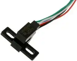
OPB933W55Z
OPTICAL SENSOR TRANSMISSIVE / SLOTTED INTERRUPTER
⚠️ Reference pricing provided. In case of supply shortages, we will connect you with our trusted procurement partners to ensure your project's continuity.
- Manufacturer: TT ELECTRONICS / OPTEK TECHNOLOGY
- Product type: Transmissive Photo Interrupters
- Gap Width: 3.18mm
- Product Range: OPB930 (L and W) Series
- Sensor Output: Open Collector
- Aperture Width: 1.27mm
- Forward Voltage: 1.7V
- Sensor Mounting: Panel / Chassis
- Forward Current If: 40mA
- Reverse Voltage Vr: 2V
| Delivery and price | |
|---|---|
| Units per pack | 250 |
| Price | 4.98 € |
| Current stock | 50+ |
| Lead time | 7 days |
Datasheet

## Features: Choice of aperture size Choice of output configurations Choice of opaque or IR transmissive shell Choice of pins (L) or wires (W) **==> picture [90 x 85] intentionally omitted <==** **----- Start of picture text -----**<br> L Package<br>Ih 1]<br>W Package<br>**----- End of picture text -----**<br> 0.125” (3.18 mm) slot width 0.320” (8.128 mm) lead spacing for PCBoard (side mounting) Data rates to 250 kBaud The **OPB930** and **OPB940** series of Photologic® photo integrated circuit switches provide optimum flexibility for the design engineer. Building from a standard housing with a 0.125” (3.18 mm) wide slot, a user can specify the type and polarity of TTL output, discrete shell material, aperture width and either 0.350” (8.9 mm) long pins **(L Series)** or 24” (610 mm) AWG, UL listed wire leads **(W Series)** . All housings are made from an opaque grade of injection-molded plastic that minimizes the assembly’s sensitivity to both visible and near-infrared ambient radiation. Discrete shells (exposed on the parallel faces inside the device throat) are either IR transmissive plastic (for applications where aperture contamination may occur) or opaque plastic (for maximum protection against ambient light). Electrical output can be specified as either TTL Totem Pole or TTL Open Collector, either of which can be supplied with buffer or inverter output polarity. All devices have the added stability of a built-in hysteresis amplifier. Custom electrical, wire and cabling and connectors are available. Contact your local representative or OPTEK for more information. - Mechanical switch replacement - Speed indication (tachometer) - Mechanical limit indication - Edge sensing ## **Part Number Guide — OPB930 and OPB940 Series** **==> picture [466 x 187] intentionally omitted <==** **----- Start of picture text -----**<br> OPB 9 X X X X X Z———————For “W” series only<br>Optek Assembly Sensor Aperture:<br>1 — 0.010” (2.54 mm)<br>5 — 0.050” (12.70 mm)<br>Photologic® Photo Integrated Emitter Aperture:<br>Circuit Sensor Family 5 — 0.050” (12.70 mm)<br>Discrete Shell Material: Mounting configurations:<br>3 — Side mount IR transmissive L — Solder leads termination<br>Plastic discrete shell W — Wire termination<br>4 — Side mount opaque Electrical Specification Variations:<br>Plastic discrete shell 0 = Buffered Totem-Pole Output<br>1 = Buffered Open-Collector Output<br>2 = Inverted Totem-Pole Output<br>3 = Inverted Open-Collector Output Industries’ Vibra-Tite<br>Vibra-Tite<br>RoHS<br>**----- End of picture text -----**<br> **CONTAINS POLYSULFONE** To avoid stress cracking, we suggest using ND Industries’ **Vibra-Tite** for thread-locking. **Vibra-Tite** evaporates fast without causing structural failure in OPTEK’s molded plastics. **==> picture [152 x 8] intentionally omitted <==** **----- Start of picture text -----**<br> OPB930, OPB940 Buffered Totem-Pole<br>**----- End of picture text -----**<br> **==> picture [167 x 9] intentionally omitted <==** **----- Start of picture text -----**<br> OPB931, OPB941 Buffered Open-Collector<br>**----- End of picture text -----**<br> **OPB932, OPB942 Inverted Totem-Pole** **OPB933 & OPB943 Inverted Open-Collector** |**OPB932, OPB942 Inverted Totem-Pole**<br>**OPB933 & OPB943 Inverted Open-Collector**<br>V<br>V<br>Anode<br>Bz O *CC<br>Anode<br>© ©cc<br>Cathode<br>=<br>OGND<br>Cathode<br>OGND|**OPB932, OPB942 Inverted Totem-Pole**<br>**OPB933 & OPB943 Inverted Open-Collector**<br>V<br>V<br>Anode<br>Bz O *CC<br>Anode<br>© ©cc<br>Cathode<br>=<br>OGND<br>Cathode<br>OGND| |---|---| |Cathode<br>=<br>O GND<br>Cathode<br>O GND<br>Absolute Maximum Ratings (T,= 25°C unlessotherwise noted)|| |Supply Voltage, VCC(not to exceed 3 seconds)|10 V| |Operating Temperature Range|-40°C to +70° C| |Storage Temperature Range|-40°C to +85° C| |Lead Soldering Temperature (1/16 inch (1.6mm) from the case for 5 sec. with soldering iron(1)|260° C| ||| |Input Diode Power Dissipation(2)|100 mW| |Output Photologic® Power Dissipation(3)|200 mW| |Total Device Power Dissipation(4)|300 mW| ||| |Voltage at Output Lead (Open Collector Output)|35 V| |Diode Forward DC Current|40 mA| |Diode Reverse DC Voltage|2 V| ## Notes: (1) RMA flux is recommended. Duration can be extended to 10 seconds maximum when flow soldering. (2) Derate linearly 2.22 mW/°C above 25°. (3) Derate linearly 4.44 mW/°C above 25°. (4) Derate linearly 6.66 mW/°C above 25°. (5) OPB930L/OPB940L series devices are terminated with 0.020” square leads designed for PCBoard mounting. (6) Methanol and isopropanol are recommended as cleaning agents. Plastic housing is soluble in chlorinated hydrocarbons and ketones. (7) All parameters tested using pulse technique. |**Color- Pin # Description**<br>Red—1<br>Black—2|**Color- Pin # Description**<br>Anode<br>Cathode|**PCBoard (L) version**|**PCBoard (L) version**| |---|---|---|---| |White—3<br>Blue—4|VCC<br>Output||| |Green—5|Ground|**DIMENSIONS ARE IN:**|**INCHES**<br>**[ MILLIMETERS]**| ## **Wired (W) version** The W Series includes wire terminations of 24” (610 mm) 7-strand, 26 AWG UL insulated wire on each terminal. Each device incorporates a wire strain relief at the housing surface. The insulation functions and colors are: anode (red), cathode (black), phototransistor collector (white) and phototransistor emitter (green). |Electrical Characteristics (T,= 25° C unless otherwise noted)<br>~~‘svwsou |~~<br>~~ataMener~~<br>~~|MIN|TWP[Max|UNITS |~~<br>~~TESTCONDITIONS|~~|Electrical Characteristics (T,= 25° C unless otherwise noted)<br>~~‘svwsou |~~<br>~~ataMener~~<br>~~|MIN|TWP[Max|UNITS |~~<br>~~TESTCONDITIONS|~~|Electrical Characteristics (T,= 25° C unless otherwise noted)<br>~~‘svwsou |~~<br>~~ataMener~~<br>~~|MIN|TWP[Max|UNITS |~~<br>~~TESTCONDITIONS|~~|Electrical Characteristics (T,= 25° C unless otherwise noted)<br>~~‘svwsou |~~<br>~~ataMener~~<br>~~|MIN|TWP[Max|UNITS |~~<br>~~TESTCONDITIONS|~~|Electrical Characteristics (T,= 25° C unless otherwise noted)<br>~~‘svwsou |~~<br>~~ataMener~~<br>~~|MIN|TWP[Max|UNITS |~~<br>~~TESTCONDITIONS|~~|Electrical Characteristics (T,= 25° C unless otherwise noted)<br>~~‘svwsou |~~<br>~~ataMener~~<br>~~|MIN|TWP[Max|UNITS |~~<br>~~TESTCONDITIONS|~~|Electrical Characteristics (T,= 25° C unless otherwise noted)<br>~~‘svwsou |~~<br>~~ataMener~~<br>~~|MIN|TWP[Max|UNITS |~~<br>~~TESTCONDITIONS|~~| |---|---|---|---|---|---|---| |~~‘svwsou |~~|~~|~~<br>~~ataMener~~<br>~~|~~|~~|MIN|~~|~~MIN|TWP[Max~~|~~[Max|~~|~~|UNITS |~~|~~|~~<br>~~TESTCONDITIONS|~~| |~~‘svwsou |~~<br>~~ataMener~~<br>~~| MIN| TWP [Max| UNITS |~~<br>~~TESTCONDITIONS |~~||||||| |VF|Forward Voltage|-|-|1.7|V|IF= 20 mA| |IR|Reverse Current|-|-|100|µA|VR= 2.0 V| |||||||| |VCC|Operating D.C. Supply Voltage|4.75|-|5.25|V|-| |ICCL|Low Level Supply Current:<br>Totem Pole & Open-Collector|-|-|15|mA|VCC= 5.25, IF= 0 mA(1)| ||Inverted Totem-Pole &<br>Inverted Open-Collector|-|-|15|mA|VCC= 5.25, IF= 15 mA| |ICCH|High Level Supply Current:<br>Totem Pole & Open-Collector|-|-|15|mA|VCC= 5.25, IF= 15 mA| ||Inverted Totem-Pole &<br>Inverted Open-Collector|-|-|15|mA|VCC= 5.25, IF= 0 mA(1)| |VOL|Low Level Output Voltage:<br>Totem Pole & Open-Collector|-|-|0.4|V|VCC= 4.75, IOL= 12.8 mA, IF= 0 mA<br>(1)| ||Inverted Totem-Pole &<br>Inverted Open-Collector|-|-|0.4|V|VCC= 4.75, IOL= 12.8 mA, IF= 15 mA| |VOH|High Level Output Voltage:<br>Totem-Pole & Open-Collector|2.4|-|-|V|VCC= 4.75, IOH= -800 µA, IF= 15 mA| ||Inverted Totem-Pole &<br>Inverted Open-Collector|2.4|-|-|V|VCC= 4.75, IOH= -800 µA, IF= 0 mA<br>(1)| |IOH|High Level Output Current:<br>Totem Pole & Open-Collector|-|-|100|µA|VCC= 4.75, VOH= 30 V, IF= 15 mA,| ||Inverted Totem-Pole &<br>Inverted Open-Collector|-|-|100|µA|VCC= 4.75, VOH= 30 V, IF= 0 mA(1)| |IF(+)|LED Positive-Going Threshold Current|-|-|15|mA|VCC= 5.0 V| |IF(+), IF(-) Hysteresis|(-) Hysteresis|-|2.0|-|V|VCC= 5.0 V| |IOS|Short Circuit Output Current:<br>Totem Pole & Open-Collector|-15|-|-60|mA|VCC= 5.25 V, IF= 15 mA, Output =<br>GND| ||Inverted Totem-Pole &<br>Inverted Open-Collector|-15|-|-60|mA|VCC= 5.25 V, IF= 0 mA(1), Output =<br>GND| |Electrical Characteristics (T,= 25° C unless otherwise noted)<br>~~-sywaot|~~<br>~~PARAMETER~~<br>~~|MIN|T¥P|Max|UNITS |~~<br>~~TEST.CONDITIONS|~~|Electrical Characteristics (T,= 25° C unless otherwise noted)<br>~~-sywaot|~~<br>~~PARAMETER~~<br>~~|MIN|T¥P|Max|UNITS |~~<br>~~TEST.CONDITIONS|~~|Electrical Characteristics (T,= 25° C unless otherwise noted)<br>~~-sywaot|~~<br>~~PARAMETER~~<br>~~|MIN|T¥P|Max|UNITS |~~<br>~~TEST.CONDITIONS|~~|Electrical Characteristics (T,= 25° C unless otherwise noted)<br>~~-sywaot|~~<br>~~PARAMETER~~<br>~~|MIN|T¥P|Max|UNITS |~~<br>~~TEST.CONDITIONS|~~|Electrical Characteristics (T,= 25° C unless otherwise noted)<br>~~-sywaot|~~<br>~~PARAMETER~~<br>~~|MIN|T¥P|Max|UNITS |~~<br>~~TEST.CONDITIONS|~~|Electrical Characteristics (T,= 25° C unless otherwise noted)<br>~~-sywaot|~~<br>~~PARAMETER~~<br>~~|MIN|T¥P|Max|UNITS |~~<br>~~TEST.CONDITIONS|~~|Electrical Characteristics (T,= 25° C unless otherwise noted)<br>~~-sywaot|~~<br>~~PARAMETER~~<br>~~|MIN|T¥P|Max|UNITS |~~<br>~~TEST.CONDITIONS|~~| |---|---|---|---|---|---|---| |~~-sywaot|~~|~~|~~<br>~~PARAMETER~~<br>~~|~~|~~|MIN|~~|~~|T¥P|~~|~~|Max|~~|~~|UNITS |~~|~~|~~<br>~~TEST.CONDITIONS|~~| |trtr<br>~~-sywaot |~~|Output Rise Time, Output Fall Time<br>~~|~~<br>~~PARAMETER~~<br>~~|~~|-<br>~~| MIN |~~|70<br>~~| T¥P |~~|-<br>~~| Max |~~|ns<br>~~| UNITS |~~|VCC= 5 V, IF= 0 or 15 mA<br>~~|~~<br>~~TEST.CONDITIONS |~~| |TPLH|Propagation Delay Low-High|-|5.0|-|µs|RL= 8TTL loads (Totem Pole)| |TPHL|Propagation Delay High-Low|-|5.0|-|µs|RL= 360 Ω (Open-Collector)| Notes: (1) Normal application would be with light source blocked, simulated by IF = 0 mA. (2) All parameters are tested using pulse techniques. **==> picture [504 x 265] intentionally omitted <==** **----- Start of picture text -----**<br> OPB930_11, OPB940_11 - Flag Next to Emitter OPB930_11, OPB940_11 - Flag Next to Sensor<br>1.20 1.20<br>1.00 1.00<br>|<br>: Right to Left | Right to Left<br>Right to Left (back)<br>Right to Left (back)<br>0.80 0.80<br>|<br>0.60 Bottom to TopTop to Bottom ol | | 0.60 Bottom to Top Top to Bottom<br>|<br>|<br>Left to Right Left to Right<br>0.40 al _— Left to Right (back) 0.40 mie Left to Right (back)<br>|<br>|<br>0.20 0.20<br>|<br>|<br>0.00 i 0.0 0<br>0.00 0.05 0.10 0.15 0.20 0.25 0.00 0.05 0.10 0.15 0.20 0.25<br>Displacement Distance (inches) Displacement Distance (inches)<br>Logic Logic<br>**----- End of picture text -----**<br> **==> picture [207 x 10] intentionally omitted <==** **----- Start of picture text -----**<br> OPB930_11, OPB940_11 - Flag in Middle of Slot<br>**----- End of picture text -----**<br> **==> picture [443 x 256] intentionally omitted <==** **----- Start of picture text -----**<br> 1.20<br>1.00<br>Right to Left<br>Right to Left (back)<br>Top to Bottom<br>0.80 0<br>Top to Bottom<br>Bottom to Top<br>0.60<br>Left to Right<br>0.40 Left to Right (back) Emitter<br>| C1<br>Left to Right Right to Left<br>———><br>0.20 [al<br>Sensor<br>|<br>0 Width<br>0.00<br>0.00 0.05 0.10 0.15 0.20 0.25<br>Displacement Distance (inches)<br>Logic<br>**----- End of picture text -----**<br> **==> picture [504 x 553] intentionally omitted <==** **----- Start of picture text -----**<br> OPB930_51, OPB940_51 - Flag Next to Emitter OPB930_51, OPB940_51 - Flag Next to Sensor<br>1.20 1.20<br>1.00 1.00<br>Right to Left Right to Left<br>Right to Left (back) Right to Left (back)<br>0.80 0.80<br>'<br>'<br>t<br>Top to Bottom md Top to Bottom<br>0.60 0.60<br>Bottom to Top Bottom to Top<br>' 1<br>Left to Right Left to Right<br>0.40 0.40<br>Left to Right (back) Left to Right (back)<br>0.20 0.20<br>0.00 0.00<br>0.00 0.05 0.10 0.15 0.20 0.25 0.00 0.05 0.10 0.15 0.20 0.25<br>Displacement Distance (inches) Displacement Distance (inches)<br>OPB930_51, OPB940_51 - Flag in Middle of Slot<br>1.20<br>1.00<br>Right to Left<br>Right to Left (back)<br>Top to Bottom<br>0.80 0<br>Top to Bottom<br>0.60 aa Bottom to Top<br>Left to Right<br>0.40 Emitter<br>Left to Right (back)<br>Left to Right Right to Left<br>0.20<br>Sensor<br>0 Width<br>0.00<br>0.00 0.05 0.10 0.15 0.20 0.25<br>Displacement Distance (inches)<br>Logic<br>Logic Logic<br>**----- End of picture text -----**<br> **==> picture [504 x 269] intentionally omitted <==** **----- Start of picture text -----**<br> OPB930_55, OPB940_55 - Flag Next to Emitter OPB930_55, OPB940_55 - Flag Next to Sensor<br>1.20 1.20<br>1.00 1.00<br>Right to Left<br>Right to Left Right to Left (back)<br>Right to Left (back)<br>0.80 0.80<br>ee eee ee<br>Top to Bottom<br>Top to Bottom<br>0.60 Bottom to Top 0.60 Bottom to Top<br>Left to Right<br>0.40 Left to Right 1°, 0.40 + Left to Right (back)<br>Left to Right (back)<br>0.20 0.20<br>0.00 0.00<br>0.00 0.05 0.10 0.15 0.20 0.25 0.00 0.05 0.10 0.15 0.20 0.25<br>Displacement Distance (inches) Displacement Distance (inches)<br>Logic Logic<br>**----- End of picture text -----**<br> **==> picture [207 x 9] intentionally omitted <==** **----- Start of picture text -----**<br> OPB930_55, OPB940_55 - Flag in Middle of Slot<br>**----- End of picture text -----**<br> **==> picture [250 x 256] intentionally omitted <==** **----- Start of picture text -----**<br> 1.20<br>1.00<br>Right to Left<br>Right to Left (back)<br>0.80<br>Top to Bottom<br>0.60 Bottom to Top<br>Left to Right<br>0.40 Left to Right (back)<br>0.20<br>0.00<br>0.00 0.05 0.10 0.15 0.20 0.25<br>Displacement Distance (inches)<br>Logic<br>**----- End of picture text -----**<br> **==> picture [138 x 156] intentionally omitted <==** **----- Start of picture text -----**<br> Top to Bottom<br>0<br>Emitter<br>| C1<br>Left to Right Right to Left<br>[al<br>Sensor<br>0 Width<br>**----- End of picture text -----**<br>
Updated at February 9, 2023
About Novapart
Novapart is a B2B electronic component broker specialising in stock shortages and cost reduction. We source hard-to-find parts and identify compliant alternatives across a catalogue of 410,000+ components from 500+ manufacturers.
Learn more →Stock Shortage Specialist
When a component is unavailable, discontinued or has an unacceptable lead time, we tap into our network of vetted European and Asian distributors to source what you need — without compromising on quality or traceability.
Request a quote →Compliant Alternatives
We identify pin-to-pin, electrically equivalent substitutes that meet the same certifications (RoHS, AEC-Q100, REACH) as your original specification — validated against datasheets, not just part numbers. Often at a lower cost.
BOM Analysis service →