
Image not available
Illustrative purposes only

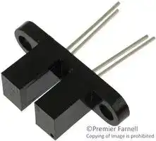
OPB866T51
OPTICAL SWITCH, 3.18MM, PHOTOTRANSISTOR
⚠️ Reference pricing provided. In case of supply shortages, we will connect you with our trusted procurement partners to ensure your project's continuity.
- Manufacturer: TT ELECTRONICS / OPTEK TECHNOLOGY
- Product type: Transmissive Photo Interrupters
- Gap Width: 3.18mm
- Sensor Output: Phototransistor
- Aperture Width: 1.27mm
- Forward Voltage: 1.3V
- Sensor Mounting: Through Hole
- Forward Current If: 50mA
- Reverse Voltage Vr: 2V
| Delivery and price | |
|---|---|
| Units per pack | 500 |
| Price | 2.28 € |
| Current stock | 200+ |
| Lead time | 7 days |
Datasheet

- Features: - 0.125” (3.175 mm) slot width - Choice of aperture (0.050” or 0.010” width) - Choice of opaque or IR transmissive shell material - Choice of mounting configurations - Choice of lead spacing or wires The slotted optical sensors in this series provide the flexibility of a custom device from a standard product line. Building from a standard housing with a 0.125” (3.18mm) wide slot, the user can specify output logic state, output driver circuit, aperture width, aperture surface and mounting tab locations. Furthermore, an option of wire or PCB leads allows electrical interface flexibility. The device body is an opaque plastic which minimizes sensitivity to both visible and near-infrared external light sources which may impact operation. Aperture width choices provide different optical resolution for motion sensing. A covered aperture provides dust protection, while an open aperture provides maximum protection against external light sources. Phototransistor sensor devices are: OPB360, OPB370, OPB380, OPB390, OPB859, OPB860, OPB870, OPB880, OPB890. The OPB355 provides a photodiode detector, which has a lower linear output-versus-light. Wide electrical output current ranges are available. LED emissions are near-infrared (850-940nm). Custom electrical, wire and cabling services are available. Contact your local representative or OPTEK for more information. Compliant to EU RoHS Directive 2002/95/EC. **==> picture [492 x 217] intentionally omitted <==** **----- Start of picture text -----**<br> OPB360, OPB370, OPB380, OPB390<br>Applications: OPB859<br>OPB355<br> Non-contact object sensing OPB860, OPB870, OPB880, OPB890<br>1 3<br> Assembly line automation 1 3<br>e e e e<br> Machine automation<br> Equipment safety<br> Machine safety<br>Vr w yv V + ~<br>e e<br>2 4<br>2 4<br>Wire Colors<br>Color # Description<br>1 Red CONTAINS POLYSULFONE<br>2 Black To avoid stress cracking, we suggest using ND Industries’ Vibra-Tite for thread-locking. ND<br>Vibra-Tite Formula 3 evaporates fast without causing structural failure in OPTEK’s molded<br>3 White plastics.<br>4 Green Applies to: OPB360, OPB370, OPB380, OPB390<br>and OPB860, OPB870, OPB880, OPB890.<br>**----- End of picture text -----**<br> **RoHS** ## **Part Number Guide — OPB355 OPB 3 X X X** **Optek Assembly** **Phototransistor Output Family** **Mounting Configurations:** L - Emitter side mounting tab only N - No mounting tabs P - Sensor side mounting tab only T - Two mounting tabs ## **Part Number Guide — OPB360 / OPB370** **OPB 3 X X X X X** - **Optek Assembly Sensor Aperture:** 1 - 0.010” (0.254 mm) 5 - 0.050” (1.270 mm) - **Phototransistor Output Family Emitter Sensor:** 1 - 0.010” (0.254 mm) 5 - 0.050” (1.270 mm) - **Discrete Shell Material:** 6 - Covered (apertures not visible), PCB leads **Mounting Configurations:** 7 - Open (apertures visible), PCB leads L - Emitter side mounting tab only N - No mounting tabs P - Sensor side mounting tab only T - Two mounting tabs **Lead Spacer Designator:** 0 = 0.320” (8.12 mm) lead space 5 = 0.220” (5.59 mm) lead space ## **Part Number Guide — OPB380 / OPB390** **OPB 3 X 0 X X X Z** **Optek Assembly RoHS Compliant Sensor Aperture: Phototransistor Output Family** 1 - 0.010” (0.254 mm) 5 - 0.050” (1.270 mm) **Emitter Sensor: Discrete Shell Material:** 1 - 0.010” (0.254 mm) 8 - Covered (apertures not visible), Wires 5 - 0.050” (1.270 mm) 9 - Open (apertures visible), Wires **Mounting Configurations:** L - Emitter side mounting tab only N - No mounting tabs P - Sensor side mounting tab only T - Two mounting tabs ## **Part Number Guide — OPB859** ## **OPB 8 5 9** **Optek Assembly** **Phototransistor Output Family** **Emitter Aperture** : 0.050” (1.270 mm) **Sensor Aperture** : 0.050” (1.270 mm) **Mounting Configurations:** T - Two mounting tabs ## **Part Number Guide — OPB860 / OPB870** ## **OPB 8 X X X X X** **Optek Assembly** **Phototransistor Output Family** **Sensor Aperture:** 1 - 0.010” (0.254 mm) 5 - 0.050” (1.270 mm) **Emitter Sensor:** 1 - 0.010” (0.254 mm) 5 - 0.050” (1.270 mm) ## **Discrete Shell Material:** 6 - Covered (apertures not visible), PCB leads 7 - Open (apertures visible), PCB leads **Electrical Specification Variations:** 0 = Electrical Parameter A (lead spacing = 0.320”) 1 = Electrical Parameter B (lead spacing = 0.320”) - 2 = Electrical Parameter C (lead spacing = 0.320”) ## **Mounting Configurations:** L - Emitter side mounting tab only N - No mounting tabs P - Sensor side mounting tab only T - Two mounting tabs - 5 = Electrical Parameter A (lead spacing = 0.220”) 6 = Electrical Parameter B (lead spacing = 0.220”) - 7 = Electrical Parameter C (lead spacing = 0.220”) Note: Assemblies with dual 0.010” apertures are currently available with electrical parameter “A” only. ## **Part Number Guide — OPB880 / OPB890** ## **OPB 8 X X X X X Z** ## **Optek Assembly** ## **Phototransistor Output Family** ## **Discrete Shell Material:** 8 - Covered (apertures not visible), Wires 9 - Open (apertures visible), Wires ## **RoHS Compliant** **Sensor Aperture:** 1 - 0.010” (0.254 mm) 5 - 0.050” (1.270 mm) ## **Emitter Sensor:** 1 - 0.010” (0.254 mm) 5 - 0.050” (1.270 mm) **Mounting Configurations:** **Electrical Specification Variations:** 0 = Electrical Parameter A 1 = Electrical Parameter B - 2 = Electrical Parameter C L - Emitter side mounting tab only N - No mounting tabs P - Sensor side mounting tab only T - Two mounting tabs NOTE: Assemblies with dual 0.010” apertures are currently available with electrical parameter “A” only. Wires = 26AWG - 24” long. UL approved. **==> picture [111 x 9] intentionally omitted <==** **----- Start of picture text -----**<br> OPB355, OPB360, OPB370<br>**----- End of picture text -----**<br> ## **OPB859** |**Pin #**|**Emitter **|**Pin #**|**Transistor/Diode**| |---|---|---|---| |1|Anode|3|Collector / Anode| |2|Cathode|4|Emitter / Cathode| **OPB380, OPB390** **OPB880, OPB890** **==> picture [115 x 19] intentionally omitted <==** **----- Start of picture text -----**<br> [ MILLIMETERS]<br>DIMENSIONS ARE IN:<br>INCHES<br>**----- End of picture text -----**<br> **OPB860, OPB870** |Absolute Maximum Ratings (T,= 25° C unless otherwise noted)|Absolute Maximum Ratings (T,= 25° C unless otherwise noted)| |---|---| |Storage Temperature(1) (2)<br>OPB355, OPB360, OPB370, OPB859, OPB860, OPB870 Series<br>OPB380, OPB390, OPB880, OPB890 Series|-40° C to +100° C<br>-40° C to +85° C| |Operating Temperature(1) (2)|-40° C to +85° C| |Lead Soldering Temperature(7)|260° C| |**Input LED**|| |Forward DC Current<br>OPB355, OPB360, OPB370, OPB380, OPB390, OPB859, OPB860, OPB870, OPB880, OPB890|50 mA| |Peak Forward Current (1µs pulse width, 300 pps)|1 A| |Reverse DC Voltage|2 V| |Power Dissipation(2)|75 mW| |**Output Phototransistor/Diode**|| |Cathode-Anode Reverse Voltage -OPB355|60 V| |Collector-Emitter Voltage<br>OPB360, OPB370, OPB380, OPB390, OPB859, OPB860, OPB870, OPB880, OPB890 Series|30 V| |Emitter-Collector Voltage|5 V| |Collector DC Current|30 mA| |Power Dissipation(1)|100 mW| ## Notes: - (1) For wire series (OPB380, OPB390, OPB880 and OPB890), maximum storage and operating temperature is limited by the temperature rating of the lead wires. - (2) Derate linearly 1.67 mW/° C above 25° C. - (3) For OPB355, OPB360 and OPB370, polarity is denoted by color of housing top: LED (clear); sensor (black). - (4) Cleaning agents methanol and isopropanol are recommended. Spray or wipe; do not submerge. - (5) OPB380 and OPB390 wire terminations have 24” of 7-strand 26 AWG UL approved insulated wire on each terminal. These devices incorporate a wire strain relief at the housing surface. The insulation colors and functions are: IRED anode (red); IRED cathode (black); phototransistor collector (white); phototransistor emitter (green). - (6) RMA flux is recommended. Duration can be extended to 10 seconds maximum when flow soldering. - (7) All parameters were tested using pulse technique. |Electrical Characteristics (T,= 25° C unless otherwise noted)<br>~~“syweou|~~<br>~~Parawerer|MIN|TYP|MAXUNITS|_TESTCONDITIONS~~|Electrical Characteristics (T,= 25° C unless otherwise noted)<br>~~“syweou|~~<br>~~Parawerer|MIN|TYP|MAXUNITS|_TESTCONDITIONS~~|Electrical Characteristics (T,= 25° C unless otherwise noted)<br>~~“syweou|~~<br>~~Parawerer|MIN|TYP|MAXUNITS|_TESTCONDITIONS~~|Electrical Characteristics (T,= 25° C unless otherwise noted)<br>~~“syweou|~~<br>~~Parawerer|MIN|TYP|MAXUNITS|_TESTCONDITIONS~~|Electrical Characteristics (T,= 25° C unless otherwise noted)<br>~~“syweou|~~<br>~~Parawerer|MIN|TYP|MAXUNITS|_TESTCONDITIONS~~|Electrical Characteristics (T,= 25° C unless otherwise noted)<br>~~“syweou|~~<br>~~Parawerer|MIN|TYP|MAXUNITS|_TESTCONDITIONS~~|Electrical Characteristics (T,= 25° C unless otherwise noted)<br>~~“syweou|~~<br>~~Parawerer|MIN|TYP|MAXUNITS|_TESTCONDITIONS~~| |---|---|---|---|---|---|---| |~~“syweou|~~|~~|~~<br>~~Parawerer|~~|~~|MIN|~~|~~MIN|TYP~~|~~|MAX~~|~~UNITS~~|~~|_TESTCONDITIONS~~| |**Input Transistor/Diode**(See OP240 for additional information—for reference only)<br>~~“syweou|~~<br>~~Parawerer | MIN| TYP |MAX UNITS | _TESTCONDITIONS~~||||||| |VF|Forward Voltage|-|1.3|1.8|V|IF= 20 mA| |IR|Reverse Current|-|-|100|µA|VR= 2 V| |**Output Diode — OPB355**(See OPB950 for additional information — for reference only)||||||| |VBR|Reverse Diode Breakdown Voltage|60|-|-|V|IR= 100 µA, IF= 0, EE= 0| |VFD|Forward Voltage Photodiode|-|-|1.2|V|IF= 1 mA, IF= 0, EE= 0| |ID|Reverse Dark Current|-|-|60|nA|VR= 30 V, EE= 0, IF= 0| |**Output Transistor**(See OP550 for additional information—for reference only)||||||| |V(BR)CEO|Collector-Emitter Breakdown Voltage|30|-|-|V|IC= 1 mA| |V(BR)ECO|Emitter-Collector Breakdown Voltage|5|-|-|V|IE= 100 µA| |ICEO|Collector-Emitter Dark Current|-|-|100|nA|VCE= 10 V, IF= 0, EE= 0| |**Coupled**||||||| |IL|On-State Collector Current<br>OPB355 (L, N, P, T)|10|-|200|µa|VR= 5 V, IF= 40 mA| |VCE(SAT)|Collector-Emitter Saturation Voltage<br>OPB859<br>OPB860/870/865/875 (Para. A)<br>OPB861/871/866/876 (Para. B)<br>OPB862/872/867/877 (Para. C)<br>OPB880/890/ (Para. A)<br>OPB881/891 (Para. B)<br>OPB882/892 (Para. C)|-<br>-<br>-<br>-<br>-<br>-<br>-|-<br>-<br>-<br>-<br>-<br>-<br>-|0.4<br>0.4<br>0.4<br>0.6<br>0.4<br>0.4<br>0.6|V|IC= 125 µA, IF= 20 mA<br>IC= 400 µA, IF= 20 mA<br>IC= 800 µA, IF= 20 mA<br>IC= 1800 µA, IF= 20 mA<br>IC= 400 µA, IF= 20 mA<br>IC= 800 µA, IF= 10 mA<br>IC= 1800 µA, IF= 20 mA| |IC(ON)<br>~~ae~~|On-State Collector Current<br>OPB36X, OPB37X (T, N, L, P 11)<br>OPB36X, OPB37X (T, N, L, P 51)<br>OPB36X, OPB37X (T, N, L, P 55)<br>OPB38X, OPB39X (T, N, L, P 11)<br>OPB38X, OPB39X (T, N, L, P 51)<br>OPB38X, OPB39X (T, N, L, P 55)|1.0<br>2.5<br>3.5<br>1.0<br>2.5<br>3.5|-<br>-<br>-<br>-<br>-<br>-|5<br>10<br>14<br>5<br>10<br>14|mA|VCE= 0.4 V, IF= 20 mA| ||OPB859|250|-|-|µA|VCE= 10 V, IF= 20 mA| ||OPB860/870/865/875 (Para. A)<br>OPB861/871/866/876 (Para. B)<br>OPB862/872/867/877 (Para. C)<br>OPB880/890/ (Para. A)<br>OPB881/891 (Para. B)<br>OPB882/892 (Para. C)<br>~~ae~~|0.5<br>1.0<br>1.8<br>0.5<br>1.0<br>1.8<br>~~ae~~|-<br>-<br>-<br>-<br>-<br>-<br>~~ae~~|-<br>-<br>-<br>-<br>-<br>-<br>~~ae~~|mA<br>~~ae~~|VCE= 10 V, IF= 20 mA<br>VCE= 5 V, IF= 10 mA<br>VCE= 0.6 V, IF= 20 mA<br>VCE= 10 V, IF= 20 mA<br>VCE= 5 V, IF= 10 mA<br>VCE= 0.6 V, IF= 20 mA<br>~~ae~~| **==> picture [503 x 565] intentionally omitted <==** **----- Start of picture text -----**<br> OPB355 - Flag Next to Emitter OPB355 - Flag Next to Sensor<br>1.20 1.20<br>Top to Bottom<br>Top to Bottom<br>1.00 1.00<br>0.80 0.80<br>Right to Left Left to Right Right to Left<br>Left to Right<br>0.60 aul 0.60 Z<br>)<br>0.40 0.40<br>0.20 0.20<br>0.00 0.00<br>0.00 0.05 0.10 0.15 0.20 0.25 0.00 0.05 0.10 0.15 0.20 0.25<br>Displacement Distance (inches) Displacement Distance (inches)<br>OPB355 - Flag in Middle of Slot<br>1.20<br>Top to Bottom<br>1.00 Top to Bottom<br>0<br>0.80<br>Right to Left<br>Left to Right<br>0.60<br>| Emitter<br>inl<br>0.40 | Left to Right —_—> <—— Right to Left<br>Sensor<br>0 Width<br>0.20<br>0.00<br>0.00 0.05 0.10 0.15 0.20 0.25<br>Displacement Distance (inches)<br> Response (mA)<br>C (ON)<br>Typical I<br> Response (mA)<br>C (ON)<br>Typical I<br> Response (mA)<br>C (ON)<br>Typical I<br>**----- End of picture text -----**<br> **==> picture [503 x 567] intentionally omitted <==** **----- Start of picture text -----**<br> Aperture Configuration 11 - Flag Next to Emitter OPB370T11 - Flag Next to Emitter Aperture Configuration 11 - Flag Next to Sensor OPB370T11 - Flag Next to Sensor<br>1.20 1.20<br>Top to Bottom Top to Bottom<br>1.00 — ——| 1.00 L 1 ——<br>—— | \<br>0.80 0.80<br>Right to Left<br>Left to Right<br>Left to Right Right to Left<br>0.60 m a 0.60 vy<br>\<br>A<br>0.40 0.40<br>0.20 0.20<br>0.00 0.00<br>0.00 0.05 0.10 0.15 0.20 0.25 0.00 0.05 0.10 0.15 0.20 0.25<br>Displacement Distance (inches) Displacement Distance (inches)<br>Aperture Configuration 11 - Flag in Middle of Slot OPB370T11 - Flag in Middle of Slot<br>1.20<br>Top to Bottom<br>1.00 Top to Bottom<br>0<br>0.80<br>0.60 Left to Right Ne\V : Right to Left a<br>Emitter<br>| | |<br>0.40 Left to Right —_> <—— Right to Left<br>Sensor<br>0.20 0 Width<br>0.00<br>0.00 0.05 0.10 0.15 0.20 0.25<br>Diisplacement Distance (inches)<br> Response (mA)<br>C(ON)<br>Typical I<br> Response (mA)<br>C(ON)<br>Typical I<br> Response (mA)<br>C(ON)<br>Typical I<br>**----- End of picture text -----**<br> **==> picture [502 x 571] intentionally omitted <==** **----- Start of picture text -----**<br> Aperture Configuration 51 - Flag Next to Emitter OPB370N51 - Flag in Middle of Slot Aperture Configuration 51 - Flag Next to Sensor OPB370N51 - Flag Next to Sensor<br>1.20 1.20<br>Top to Bottom<br>Top to Bottom<br>1.00 1.00<br>\<br>0.80 0.80<br>a Left to Right t+ Right to Left<br>0.60 Left to Right = Right to Left 0.60<br>|<br>\<br>0.40 0.40<br>0.20 0.20<br>0.00 0.00<br>0.00 0.05 0.10 0.15 0.20 0.25 0.00 0.05 0.10 0.15 0.20 0.25<br>Displacement Distance (inches) Displacement Distance (inches)<br>Aperture Configuration 51 - Flag in Middle of Slot OPB370N51 - Flag in Middle of Slot<br>1.20<br>Top to Bottom<br>1.00 Top to Bottom<br>0<br>0.80<br>Left to Right Right to Left<br>0.60<br>Emitter<br>| | |<br>0.40 | Left to Right —> <—— Right to Left<br>TC<br>Sensor<br>0 Width<br>0.20<br>0.00<br>0.00 0.05 0.10 0.15 0.20 0.25<br>Displacement Distance (inches)<br> Response (mA) Response (mA)<br>C(ON) C(ON)<br>Typical I Typical I<br> Response (mA)<br>C(ON)<br>Typical I<br>**----- End of picture text -----**<br> **==> picture [504 x 571] intentionally omitted <==** **----- Start of picture text -----**<br> Aperture Configuration 55 - Flag Next to Emitter OPB380T55 - Flag Next to Emitter Aperture Configuration 55 - Flag Next to Sensor OPB380T55 - Flag Next to Sensor<br>1.20 1.20<br>Top to Bottom Top to Bottom<br>1.000.80 i eee 1.000.80 eee<br>Right to Left Left to Right Right to Left<br>Left to Right<br>0.60 eG 0.60<br>/ a en 0<br>0.40 ee 0.40 aw,<br>0.20 ee e e 0.20 e e (ee<br>G e e<br>0.00 0.00<br>0.00 0.05 0.10 0.15 0.20 0.25 0.00 0.05 0.10 0.15 0.20 0.25<br>Displacement Distance (inches) Displacement Distance (inches)<br>Aperture Configuration 55 - Flag in Middle of Slot OPB380T55 - Flag in Middle of Slot<br>1.20<br>Top to Bottom<br>1.00 Top to Bottom<br>0<br>0.80 Sa<br>0.60 Left to Right [ Right to Left<br>ee /ee - Emitter<br>\ Left to Right —_> < —__——_. Right to Left<br>0.40 I<br>Sensor<br>0 Width<br>0.20<br>0.00 fh<br>0.00 0.05 0.10 0.15 0.20 0.25<br>Displacement Distance (inches)<br> Response (mA) Response (mA)<br>C(ON) C(ON)<br>Typical I Typical I<br> Response (mA)<br>C(ON)<br>Typical I<br>**----- End of picture text -----**<br>
Updated at February 9, 2023
About Novapart
Novapart is a B2B electronic component broker specialising in stock shortages and cost reduction. We source hard-to-find parts and identify compliant alternatives across a catalogue of 420,000+ components from 500+ manufacturers.
Learn more →Stock Shortage Specialist
When a component is unavailable, discontinued or has an unacceptable lead time, we tap into our network of vetted European and Asian distributors to source what you need — without compromising on quality or traceability.
Request a quote →Compliant Alternatives
We identify pin-to-pin, electrically equivalent substitutes that meet the same certifications (RoHS, AEC-Q100, REACH) as your original specification — validated against datasheets, not just part numbers. Often at a lower cost.
BOM Analysis service →