
Image not available
Illustrative purposes only

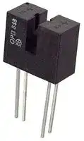
OPB848
SLOTTED SWITCH, TRANSISTOR
⚠️ Reference pricing provided. In case of supply shortages, we will connect you with our trusted procurement partners to ensure your project's continuity.
- Manufacturer: TT ELECTRONICS / OPTEK TECHNOLOGY
- Product type: Transmissive Photo Interrupters
- Gap Width: 2.54mm
- Product Range: OPB848 Series
- Sensor Output: Phototransistor
- Aperture Width: 0.635mm
- Forward Voltage: 1.7V
- Sensor Mounting: Through Hole
- Forward Current If: 50mA
- Reverse Voltage Vr: 2V
| Delivery and price | |
|---|---|
| Units per pack | 500 |
| Price | 1.87 € |
| Current stock | 10+ |
| Lead time | 20 days |
Datasheet

## Slotted Optical Switch

## OPB847, OPB848

## **Features:**

- Non-contact switching

- Apertured for high resolution

- Hermetically sealed components

## **Description:**

The OPB847 and OPB848 consists of a gallium aluminum arsenide LED and a silicon phototransistor, which is soldered into a printed PCBoard and mounted in a high-temperature plastic housing on opposite sides of a 0.100 inch (2.540 mm) wide slot. Both device types have a .025 (0.635mm) inch by .060 inch (1.524 mm) aperture in front of the phototransistor for high resolution positioning sensing.  Phototransistor switching takes place when an opaque object passes through the slot.

## **Applications:**

- Non-contact interruptive object sensing

- Assembly line automation

- Machine automation

|**Part Number**|**LED Peak**<br>**Wavelength**|**Wavelength**<br>**Sensor**|**Slot Width /**<br>**Depth**|**Aperture**<br>**Emitter/Sensor**|**Emitter/Sensor**<br>**Lead Length /**<br>**Spacing**|
|---|---|---|---|---|---|
|**OPB847**|890 nm|Transistor|Transistor<br>0.100" / 0.250”|0.100" / 0.250” 0.025" / 0.025"|0.025" / 0.025" 0.425" / 0.300"|
|**OPB848**||||||


- Equipment security

- Machine safety

**==> picture [54 x 84] intentionally omitted <==**

**----- Start of picture text -----**<br>
1  4<br>y BN<br>|<br>2  3<br>**----- End of picture text -----**<br>


|**Pin #**|**Description**|
|---|---|
|1|Anode|
|2|Cathode|
|3|Emitter|
|4|Collector|


**==> picture [116 x 55] intentionally omitted <==**

**----- Start of picture text -----**<br>
[ MILLIMETERS]<br>DIMENSIONS ARE IN:<br>| INCHES<br>**----- End of picture text -----**<br>


**==> picture [31 x 8] intentionally omitted <==**

**----- Start of picture text -----**<br>
RoHS<br>**----- End of picture text -----**<br>


General Note TT Electronics reserves the right to make changes in product specification without notice or liability.  All information is subject to TT Electronics’ own data and is considered accurate at time of going to print.

TT Electronics | Optek Technology, Inc. 1645 Wallace Drive, Ste. 130, Carrollton, TX USA 75006 |Ph: +1 972 323 2200 www.ttelectronics.com | sensors@ttelectronics.com

Issue A     11/2016     Page 1

© TT electronics plc

## Slotted Optical Switch

## OPB847, OPB848

## **Electrical Specifications**

**Absolute Maximum Ratings** (TA = 25° C unless otherwise noted)

Operating and Storage Temperature Range -40° C to +85° C Lead Soldering Temperature [1/16 inch (1.6mm) from the case for 5 sec. with soldering iron] 240° C ~~ee~~ **Input Diode** Forward DC Current 50 mA Reverse Voltage 2.0 V Power Dissipation[(2)] 100 mW ~~eo~~ **Output Phototransistor** Collector-Emitter Voltage 30 V Emitter-Collector Voltage 7 V Power Dissipation[(2)] 100 mW

## **Electrical Characteristics** (TA = 25° C unless otherwise noted)

|**Electrical Characteristics**|**Electrical Characteristics**|**Electrical Characteristics **(TA = 25° C unless otherwise noted)A = 25° C unless otherwise noted)= 25° C unless otherwise noted)|(TA = 25° C unless otherwise noted)A = 25° C unless otherwise noted)= 25° C unless otherwise noted)|(TA = 25° C unless otherwise noted)A = 25° C unless otherwise noted)= 25° C unless otherwise noted)||||
|---|---|---|---|---|---|---|---|
|**SYMBOL**<br>**Input Diode**<br>~~a~~||**PARAMETER**<br>**Input Diode**|**MIN**|**TYP**|**MAX**|**UNITS**|**TEST CONDITIONS**|
||||1.00|1.35|1.70||IF= 20 mA|
||VF|Forward Voltage(4)|1.20|1.55|1.90|V|IF= 20 mA, TA= -55° C|
||||1.80|1.20|1.60||IF= 20 mA, TA= 100° C|
||IR|Reverse Current|-|0.10|100|µA|VR= 2 V|
||**Output Phototransistor**|||||||
||V(BR)CEO|Collector-Emitter Breakdown Voltage|30|110|-|V|IC= 100 µA, IF= 0|
||V(BR)ECO|Emitter-Collector Breakdown Voltage|5|10|-|V|IE= 100 µA, IF= 0|
||||-|0.20|100|nA|VCE= 10 V, IF= 0|
||ICEO|Collector-Emitter Dark Current||||||
||||-|10|100|µA|VCE= 10 V, IF= 0, TA= 100° C|


Notes:

(1) Duration can be extended to 10 seconds maximum when flow soldering.

- (2) Derate linearly 1.00 mW/° C above 25° C.

(3) Methanol and isopropanol are recommended as cleaning agents.

(4) Measurement is taken during the last 500 µs of a single 1.0 ms test pulse.  Heating due to increased pulse rate or pulse width can cause change in measurement results.

General Note

TT Electronics | Optek Technology, Inc. 1645 Wallace Drive, Ste. 130, Carrollton, TX USA 75006 |Ph: +1 972 323 2200 www.ttelectronics.com | sensors@ttelectronics.com

TT Electronics reserves the right to make changes in product specification without notice or liability.  All information is subject to TT Electronics’ own data and is considered accurate at time of going to print.

Issue A     11/2016     Page 2

© TT electronics plc

## Slotted Optical Switch

## OPB847, OPB848

**Electrical Characteristics** (TA = 25° C unless otherwise noted)

|**Combined**||||||
|---|---|---|---|---|---|
|IC(ON)|On-State Collector Current(1)<br>OPB847<br>OPB848|4.0<br>1.0<br>-<br>-|-<br>-<br>-<br>-|mA|VCE= 10 V, IF= 20 mA<br>VCE= 10 V, IF= 20 mA|
|VCE(SAT)|Collector-Emitter Saturation Voltage<br>OPB847<br>OPB848|0.30<br>0.30|0.30<br>0.30<br>0.40<br>0.40|V|IC= 2 mA, IF= 20 mA<br>IC= 500 µA, IF= 20 mA|
|tr|Output Rise Time<br>OPB847<br>OPB848|12<br>8|12<br>8<br>20<br>15|µs|VCC= 10 V, IF= 20 mA, RL= 1000Ω|
|tf<br>Notes:|Output Fall Time<br>OPB847<br>OPB848|12<br>8|12<br>8<br>20<br>15|||


Notes:

(1) Measurement is taken during the last 500 µs of a single 1.0 ms test pulse.  Heating due to increased pulse rate or pulse width can cause change in measurement results.

**==> picture [507 x 335] intentionally omitted <==**

**----- Start of picture text -----**<br>
OPB847 - Flag Next to Emitter OPB847 - Flag Next to Sensor<br>1.201.00 TP. 1.201.00<br>0.80 0.80<br>0.60 Ap 0.60<br>0.40 0.40<br>Right to Left Right to Left<br>0.20 Left to Right 0.20 Left to Right<br>Top to Bottom Top to Bottom<br>0.00 —AAY\e 0.00 aan|<br>0.00 0.05 0.10 0.15 0.20 0.25 0.00 0.05 0.10 0.15 0.20 0.25<br>Displacement Distance (inches) OPB847 - Flag in Middle of Slot Displacement Distance (inches)<br>1.20<br>1.00<br>0.80<br>0.60<br>0.40<br>Right to Left<br>0.20 Left to Right<br>Top to Bottom<br>0.00<br>0.00 0.05 0.10 0.15 0.20 0.25<br>Displacement Distance (inches)<br> Response (mA)<br>C(ON)<br>Typical I<br> Response (mA)<br>C(ON)<br>Typical I<br> Response (mA)<br>C(ON)<br>Typical I<br>**----- End of picture text -----**<br>


General Note TT Electronics reserves the right to make changes in product specification without notice or liability.  All information is subject to TT Electronics’ own data and is considered accurate at time of going to print.

TT Electronics | Optek Technology, Inc. 1645 Wallace Drive, Ste. 130, Carrollton, TX USA 75006 |Ph: +1 972 323 2200 www.ttelectronics.com | sensors@ttelectronics.com

Issue A     11/2016     Page 3

© TT electronics plc
Updated at February 9, 2023
About Novapart
Novapart is a B2B electronic component broker specialising in stock shortages and cost reduction. We source hard-to-find parts and identify compliant alternatives across a catalogue of 420,000+ components from 500+ manufacturers.
Learn more →Stock Shortage Specialist
When a component is unavailable, discontinued or has an unacceptable lead time, we tap into our network of vetted European and Asian distributors to source what you need — without compromising on quality or traceability.
Request a quote →Compliant Alternatives
We identify pin-to-pin, electrically equivalent substitutes that meet the same certifications (RoHS, AEC-Q100, REACH) as your original specification — validated against datasheets, not just part numbers. Often at a lower cost.
BOM Analysis service →