
Image not available
Illustrative purposes only

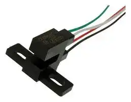
OPB842W51Z
Transmissive Photo Interrupter, Phototransistor, Panel Mount, 3.18 mm, 1.27 mm, 50 mA, 2 V
⚠️ Reference pricing provided. In case of supply shortages, we will connect you with our trusted procurement partners to ensure your project's continuity.
- Manufacturer: TT ELECTRONICS / OPTEK TECHNOLOGY
- Product type: Transmissive Photo Interrupters
- Gap Width: 3.18mm
- Product Range: OPB840 Series
- Sensor Output: Phototransistor
- Aperture Width: 1.27mm
- Forward Voltage: 1.7V
- Sensor Mounting: Panel Mount
- Forward Current If: 50mA
- Reverse Voltage Vr: 2V
| Delivery and price | |
|---|---|
| Units per pack | 50 |
| Price | 4.45 € |
| Current stock | 10+ |
| Lead time | 30 days |
Datasheet

## Slotted Optical Switch ## OPB830 and OPB840 (L and W) ## **Features:** - 0.125” (3.18 mm) wide slot - Choice of electrical output parameters - Choice of aperture - Choice of opaque or IR transmissive shell material - Side mount configuration - Choice of lead spacing (L Series) - 24” [610 mm] 26 AWG wire leads (W Series) **==> picture [77 x 124] intentionally omitted <==** **----- Start of picture text -----**<br> L Package<br>iv<br>W Package<br>bi<br>**----- End of picture text -----**<br> ## **Description:** OPB830 and OPB840 series provide the design engineer with the flexibility of a custom device from a standard product line. The L Series offers a choice of PCBoard mount lead spacing, while the W Series offers 24” (610mm) 26AWG wire leads. Building from a standard housing that utilizes a .375” (9.5 mm) wide slot, a user can specify the electrical output parameters, choice of aperture, discrete shell material, side mount configuration, and a choice of lead spacing (for the L Series) or 24” [610 mm] UL approved 26 AWG wire leads (W Series). Housings are made from an opaque grade of injection-molded plastic that minimizes the assembly’s sensitivity to visible and near-infrared ambient radiation. Discrete shells (exposed on the parallel faces inside the device throat) are made of either IR transmissive plastic (for applications where aperture contamination may occur) or of opaque plastic with aperture openings (for maximum protection against ambient light). Switching of the phototransistor occurs whenever an opaque object passes through the slot and interrupts the beam. ## **Applications:** - Non-contact interruptive object sensing - Assembly line automation - Machine automation - Equipment security - Machine safety > TT Electronics | Optek Technology, Inc. 1645 Wallace Drive, Ste. 130, Carrollton, TX USA 75006 |Ph: +1 972 323 2200 www.ttelectronics.com | sensors@ttelectronics.com General Note TT Electronics reserves the right to make changes in product specification without notice or liability. All information is subject to TT Electronics’ own data and is considered accurate at time of going to print. Issue A 11/2016 Page 1 © TT electronics plc ## Slotted Optical Switch OPB830 and OPB840 (L and W) ## **Electrical Specifications** **Absolute Maximum Ratings** (TA=25°C unless otherwise noted) |**Absolute Maximum Ratings**(TA=25°C unless otherwise noted)A=25°C unless otherwise noted)=25°C unless otherwise noted)|**Absolute Maximum Ratings**(TA=25°C unless otherwise noted)A=25°C unless otherwise noted)=25°C unless otherwise noted)|**Absolute Maximum Ratings**(TA=25°C unless otherwise noted)A=25°C unless otherwise noted)=25°C unless otherwise noted)| |---|---|---| |Storage and Operating Temperature<br>L Series(1)<br>W Series(1)<br>-40° C to +85°C<br>-40° C to +80°C<br>Lead Soldering Temperature [1/16 inch (1.6mm) from the case for 5 sec. with soldering iron](2)<br>260°C<br>~~EEE~~||| ||**Input Diode**|| ||Forward DC Current|50 mA| ||Peak Forward Current (1 µs pulse width, 300 pps)|1 A| ||Reverse DC Voltage|2 V| ||Power Dissipation(1)|100 mW| ||**Output Phototransistor**|| ||Collector-Emitter Voltage|30 V| ||Emitter-Collector Voltage|5 V| ||Collector DC Current|30 mA| ||Power Dissipation(1)|100 mW| **Electrical Characteristics** (TA = 25°C unless otherwise noted) **SYMBOL PARAMETER MIN TYP MAX UNITS TEST CONDITIONS** ~~PT~~ **Input Diode LED** (See OP240 for additional information—for reference only) VF Forward Voltage - - 1.7 V IF = 20 mA IR Reverse Current - - 100 µA VR = 2 V ~~pp~~ **Output Transistor** (See OP550 for additional information—for reference only) V(BR)CEO Collector-Emitter Breakdown Voltage 30 - - V IC = 1 mA V(BR)ECO Emitter-Collector Breakdown Voltage 5 - - V IE = 100 µA ICEO Collector-Emitter Dark Current - - 100 nA VCE = 10 V ~~pe~~ - Notes: (1) Derate linearly 1.67 mW/° C above 25° C for L Series. (2) RMA flux is recommended. Duration can be extended to 10 seconds maximum when flow soldering. - (3) Methanol or isopropanol are recommended as cleaning agents. Plastic housing is soluble in chlorinated hydrocarbons and ketones. (4) The W Series includes wire terminations of 24” (610 mm) 7-strand, 26 AWG UL insulated wire on each terminal. Each device incorporates a wire strain relief at the housing surface. The insulation functions and colors are: anode (red), cathode (black), phototransistor collector (white) and phototransistor emitter (green). - (5) All parameters tested using pulse technique. ## General Note TT Electronics | Optek Technology, Inc. > 1645 Wallace Drive, Ste. 130, Carrollton, TX USA 75006 |Ph: +1 972 323 2200 www.ttelectronics.com | sensors@ttelectronics.com TT Electronics reserves the right to make changes in product specification without notice or liability. All information is subject to TT Electronics’ own data and is considered accurate at time of going to print. Issue A 11/2016 Page 2 © TT electronics plc ## Slotted Optical Switch ## OPB830 and OPB840 (L and W) ## **Electrical Characteristics** (TA = 25°C unless otherwise noted) |**Combined**||||||| |---|---|---|---|---|---|---| |VCE(SAT)|Collector-Emitter Saturation Voltage<br>Parameter A<br>(OPB830L,OPB840L)<br>(OPB835L, OPB845L)<br>(OPB830W,OPB840W)<br>(OPB835W, OPB845W)<br>Parameter B<br>(OPB831L,OPB841L)<br>(OPB836L,OPB846L)<br>(OPB831W,OPB841W)<br>(OPB836W,OPB846W)<br>Parameter C<br>(OPB832L,OPB842L)<br>(OPB837L,OPB847L)<br>(OPB832W,OPB842W)<br>(OPB837W,OPB847W)|-|-|0.4|V|IC= 400 µA, IF= 20 mA| |||-|-|0.4|V|IC= 800 µA, IF= 10 mA| |||-|-|0.6|V|IC= 1800 µA, IF= 20 mA| |IC(ON)|On-State Collector Current<br>Parameter A<br>(OPB830L,OPB840L)<br>(OPB835L, OPB845L)<br>(OPB830W,OPB840W)<br>(OPB835W, OPB845W)<br>Parameter B<br>(OPB831L,OPB841L)<br>(OPB836L,OPB846L)<br>(OPB831W,OPB841W)<br>(OPB836W,OPB846W)<br>Parameter C<br>(OPB832L,OPB842L)<br>(OPB837L,OPB847L)<br>(OPB832W,OPB842W)<br>(OPB837W,OPB847W)|0.625|-|-|mA|VCE= 10 V, IF= 20 mA| |||1.250|-|-|mA|VCE= 5 V, IF= 10 mA| |||2.250|-|-|mA|VCE= .6 V, IF= 20 mA| General Note TT Electronics | Optek Technology, Inc. 1645 Wallace Drive, Ste. 130, Carrollton, TX USA 75006 |Ph: +1 972 323 2200 www.ttelectronics.com | sensors@ttelectronics.com TT Electronics reserves the right to make changes in product specification without notice or liability. All information is subject to TT Electronics’ own data and is considered accurate at time of going to print. Issue A 11/2016 Page 3 © TT electronics plc ## Slotted Optical Switch ## OPB830 and OPB840 (L and W) **==> picture [503 x 578] intentionally omitted <==** **----- Start of picture text -----**<br> OPB8_ _ L11 - Flag Next to Emitter OPB370T11 - Flag Next to Emitter OPB8_ _ L11 - Flag Next to Sensor OPB370T11 - Flag Next to Sensor<br>1.20 1.20<br>Top to Bottom Top to Bottom<br>1.00 1.00<br>CT) Ee<br>0.80 0.80<br>Right to Left<br>os es Left to Right<br>Left to Right Right to Left<br>0.60 0.60<br>eee Gee ee<br>0.40 0.40<br>0.200.00 Pyee Ce | a= 0.200.00 ee|<br>0.00 0.05 0.10 0.15 0.20 0.25 0.00 0.05 0.10 0.15 0.20 0.25<br>Displacement Distance (inches) Displacement Distance (inches)<br>OPB8_ _ L11 - Flag in Middle of Slot OPB370T11 - Flag in Middle of Slot<br>1.20<br>Top to Bottom<br>1.00 Top to Bottom<br>pt Tf 0<br>0.80<br>Wy Left to Right Right to Left<br>0.60<br>ens (oe Emitter<br>Left to Right Right to Left<br>0.40<br>et [RE] | | ) ee<br>Sensor<br>0.20 of 0 _ Width<br>0.00 es Co<br>0.00 0.05 0.10 0.15 0.20 0.25<br>Diisplacement Distance (inches)<br> Response (mA)<br>C(ON)<br>Typical I<br> Response (mA)<br>C(ON)<br>Typical I<br> Response (mA)<br>C(ON)<br>Typical I<br>**----- End of picture text -----**<br> General Note TT Electronics reserves the right to make changes in product specification without notice or liability. All information is subject to TT Electronics’ own data and is considered accurate at time of going to print. TT Electronics | Optek Technology, Inc. 1645 Wallace Drive, Ste. 130, Carrollton, TX USA 75006 |Ph: +1 972 323 2200 www.ttelectronics.com | sensors@ttelectronics.com Issue A 11/2016 Page 4 © TT electronics plc ## Slotted Optical Switch ## OPB830 and OPB840 (L and W) **==> picture [502 x 582] intentionally omitted <==** **----- Start of picture text -----**<br> OPB8_ _ L51 - Flag Next to Emitter OPB370N51 - Flag in Middle of Slot OPB8_ _ L51 - Flag Next to Sensor OPB370N51 - Flag Next to Sensor<br>1.20 1.20<br>Top to Bottom<br>Top to Bottom<br>1.00 ee 1.00 e<br>0.80 0.80<br>Left to Right Right to Left<br>Left to Right Right to Left<br>0.60 a 0.60 ae<br>0.40 0.40<br>0.20 0.20<br>fo (ee Qeni ine<br>0.00 ee 0.00<br>0.00 0.05 0.10 | 0.15 0.20 0.25 0.00 0.05 0.10 0.15 0.20 0.25<br>Displacement Distance (inches) Displacement Distance (inches)<br>OPB8_ _ L51 - Flag in Middle of Slot OPB370N51 - Flag in Middle of Slot<br>1.20<br>Top to Bottom<br>1.00 a Top to Bottom<br>0.80 af 0 ee e<br>Left to Right Right to Left<br>0.60 oe<br>Emitter<br>Left to Right Right to Left<br>0.40 ee<br>Sensor<br>0 Width<br>0.20 ee te a<br>0.00 JL<br>0.00 0.05 0.10 0.15 0.20 0.25<br>Displacement Distance (inches)<br> Response (mA) Response (mA)<br>C(ON) C(ON)<br>Typical I Typical I<br> Response (mA)<br>C(ON)<br>Typical I<br>**----- End of picture text -----**<br> General Note TT Electronics reserves the right to make changes in product specification without notice or liability. All information is subject to TT Electronics’ own data and is considered accurate at time of going to print. TT Electronics | Optek Technology, Inc. 1645 Wallace Drive, Ste. 130, Carrollton, TX USA 75006 |Ph: +1 972 323 2200 www.ttelectronics.com | sensors@ttelectronics.com Issue A 11/2016 Page 5 © TT electronics plc ## Slotted Optical Switch ## OPB830 and OPB840 (L and W) **==> picture [504 x 584] intentionally omitted <==** **----- Start of picture text -----**<br> OPB8_ _ L55 - Flag Next to Emitter OPB380T55 - Flag Next to Emitter OPB8_ _ L55 - Flag Next to Sensor OPB380T55 - Flag Next to Sensor<br>1.20 1.20<br>Top to Bottom Top to Bottom<br>1.00 pt 1.00<br>0.80 hftT | 0.80 Ld|<br>Right to Left Left to Right Right to Left<br>Left to Right<br>0.600.40 ARee ee 0.600.40 ieev) e<br>0.20 OM 0.20<br>0.00 ee 0.00<br>A<br>0.00 0.05 0.10 0.15 0.20 0.25 0.00 0.05 0.10 0.15 0.20 0.25<br>Displacement Distance (inches) Displacement Distance (inches)<br>OPB8_ _ L55 - Flag in Middle of Slot OPB380T55 - Flag in Middle of Slot<br>1.20<br>Top to Bottom<br>1.00 ee Top to Bottom<br>0<br>0.80 2 ee e<br>e e e<br>Left to Right Right to Left<br>0.60<br>Emitter<br>oa<br>Left to Right Right to Left<br>0.40<br>Sensor<br>ee — —<br>0 Width<br>0.20<br>eee<br>0.00 J<br>0.00 0.05 0.10 0.15 0.20 0.25<br>Displacement Distance (inches)<br> Response (mA) Response (mA)<br>C(ON) C(ON)<br>Typical I Typical I<br> Response (mA)<br>C(ON)<br>Typical I<br>**----- End of picture text -----**<br> General Note TT Electronics reserves the right to make changes in product specification without notice or liability. All information is subject to TT Electronics’ own data and is considered accurate at time of going to print. TT Electronics | Optek Technology, Inc. 1645 Wallace Drive, Ste. 130, Carrollton, TX USA 75006 |Ph: +1 972 323 2200 www.ttelectronics.com | sensors@ttelectronics.com Issue A 11/2016 Page 6 © TT electronics plc ## Slotted Optical Switch OPB830 and OPB840 (L and W) ## **Packaging** **==> picture [98 x 8] intentionally omitted <==** **----- Start of picture text -----**<br> OPB830/840L Series<br>**----- End of picture text -----**<br> **==> picture [58 x 90] intentionally omitted <==** **----- Start of picture text -----**<br> 1 3<br>e<br>e<br>aN<br>~<br>e e<br>2 4<br>**----- End of picture text -----**<br> **==> picture [258 x 76] intentionally omitted <==** **----- Start of picture text -----**<br> Pin # / Color Description<br>1 / Black Cathode<br>2 / Red Anode OPB830/840W Series<br>3 / White Collector<br>4 / Green Emitter<br>**----- End of picture text -----**<br> **==> picture [116 x 15] intentionally omitted <==** **----- Start of picture text -----**<br> [ MILLIMETERS]<br>DIMENSIONS ARE IN:<br>INCHES<br>**----- End of picture text -----**<br> General Note TT Electronics reserves the right to make changes in product specification without notice or liability. All information is subject to TT Electronics’ own data and is considered accurate at time of going to print. TT Electronics | Optek Technology, Inc. 1645 Wallace Drive, Ste. 130, Carrollton, TX USA 75006 |Ph: +1 972 323 2200 www.ttelectronics.com | sensors@ttelectronics.com Issue A 11/2016 Page 7 © TT electronics plc ## Slotted Optical Switch OPB830 and OPB840 (L and W) **Part Number Guide — OPB8XX OPB 8 X X L X X Optek Assembly Sensor Aperture: 1 —** 0.010” (0.25 mm) **5 —** 0.050” (1.27 mm) **Phototransistor Output Family Emitter Aperture: 1 —** 0.010” (0.25 mm) **5 —** 0.050” (1.27 mm) **Discrete Shell Material: Mounting configurations: 3 —** Side mount IR transmissive **L —** Solder lead termination Plastic discrete shell ~~==~~ **4 —** Side mount opaque **Electrical Specification Variations:** Plastic discrete shell **0** = Electrical Parameter A - (0.320” lead spacing) **1** = Electrical Parameter B - (0.320” lead spacing) **2** = Electrical Parameter C - (0.320” lead spacing) **5** = Electrical Parameter A - (0.220” lead spacing) **6** = Electrical Parameter B - (0.220” lead spacing) **7** = Electrical Parameter C - (0.220” lead spacing) **Notes:** Assemblies with dual 0.010” apertures are currently available with electrical parameter “A” only. **Part Number Guide — OPB8XX OPB 8 X X W X X Z Optek Assembly Sensor Aperture: 1 —** 0.010” (0.25 mm) **5 —** 0.050” (1.27 mm) **Phototransistor Output Family Emitter Aperture: 1 —** 0.010” (0.25 mm) **5 —** 0.050” (1.27 mm) **Discrete Shell Material: Mounting configurations: 3 —** Side mount IR transmissive **W —** Wire termination Plastic discrete shell ~~SIE~~ **•** Parts ending with “Z” meet **4 —** Side mount opaque **Electrical Specification Variations:** RoHS requirements Plastic discrete shell **0** = Electrical Parameter A **•** Wires = 26 AWG—24” Long **1** = Electrical Parameter B **2** = Electrical Parameter C **Notes:** Assemblies with dual 0.010” apertures are currently available with electrical parameter “A” only. General Note TT Electronics reserves the right to make changes in product specification without notice or liability. All information is subject to TT Electronics’ own data and is considered accurate at time of going to print. TT Electronics | Optek Technology, Inc. 1645 Wallace Drive, Ste. 130, Carrollton, TX USA 75006 |Ph: +1 972 323 2200 www.ttelectronics.com | sensors@ttelectronics.com Issue A 11/2016 Page 8 © TT electronics plc
Updated at February 9, 2023
About Novapart
Novapart is a B2B electronic component broker specialising in stock shortages and cost reduction. We source hard-to-find parts and identify compliant alternatives across a catalogue of 420,000+ components from 500+ manufacturers.
Learn more →Stock Shortage Specialist
When a component is unavailable, discontinued or has an unacceptable lead time, we tap into our network of vetted European and Asian distributors to source what you need — without compromising on quality or traceability.
Request a quote →Compliant Alternatives
We identify pin-to-pin, electrically equivalent substitutes that meet the same certifications (RoHS, AEC-Q100, REACH) as your original specification — validated against datasheets, not just part numbers. Often at a lower cost.
BOM Analysis service →