
Image not available
Illustrative purposes only

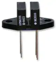
OPB822SD
Transmissive Photo Interrupter, Phototransistor, Panel / Chassis, 2.286 mm, 0.254 mm, 20 mA, 2 V
⚠️ Reference pricing provided. In case of supply shortages, we will connect you with our trusted procurement partners to ensure your project's continuity.
- Manufacturer: TT ELECTRONICS / OPTEK TECHNOLOGY
- Product type: Transmissive Photo Interrupters
- Gap Width: 2.286mm
- Product Range: OPB822SD Series
- Sensor Output: Phototransistor
- Aperture Width: 0.254mm
- Forward Voltage: 1.7V
- Sensor Mounting: Panel / Chassis
- Forward Current If: 20mA
- Reverse Voltage Vr: 2V
| Delivery and price | |
|---|---|
| Units per pack | 50 |
| Price | 4.85 € |
| Current stock | 50+ |
| Lead time | 7 days |
Datasheet

- Non-contact switching
- Features:
- Single or double apertures for high resolution
- Choice of slot widths
- Choice of side-by-side or over/under dual channels
- Choice of electrical outputs
**==> picture [77 x 98] intentionally omitted <==**
**----- Start of picture text -----**<br>
» OPB826<br>OPB822<br>**----- End of picture text -----**<br>
Each **OPB822** and **OPB826** slotted switch consists of two infrared emitting diodes and two NPN silicon phototransistors mounted on opposite sides of a 0.090” (2.29 mm) wide slot **(OPB822)** or a 0.100” (2.54 mm) wide slot **(OPB826)** .
**OPB822** uses an side-by-side mounting configuration, while **OPB826** uses an over/under mounting configuration. **OPB822S** has 0.01” by 0.04” (0.25 mm x 1.02 mm) apertures in front of both phototransistors while the **OPB822SD** has the aperture in front of both phototransistors and both emitters. The **OPB826S** has 0.04” by 0.04” (1.02 mm x 1.02 mm) apertures in front of both phototransistors while the **OPB826SD** has the aperture in front of both phototransistors and both emitters.
Dual channels enable direction of travel sensing, with the low-cost plastic housing reduces possible interference from ambient light and provides protection from dust and dirt.
Phototransistor switching occurs when an opaque object passes through the device slot.
For information on encoder design, see Application Bulletin 203 at:
|Custom electrical, wire and cabling and<br>connectors are available. Contact your local<br>representative or OPTEK for more information.<br>Encoders<br>Non-contact object sensing<br>Assembly line automation<br>Machine automation<br>Equipment security<br>Machine safety<br>—|**Part**<br>**Number**<br>**LED**<br>**Peak**<br>**Wavelength**<br>**Sensor**<br>**Slot**<br>**Width /**<br>**Depth**<br>**Aperture**<br>**Emitter/**<br>**Sensor**<br>**Lead**<br>**Length /**<br>**Spacing**<br>**OPB822S**<br>**Dual**<br>**935 nm**<br>**Dual**<br>**Transistor**<br>**0.09" /**<br>**0.30”**<br>**None /**<br>**0.01"**<br>**0.35" /**<br>**0.30"**<br>**OPB822SD**<br>**0.01" /**<br>**0.01"**<br>**OPB826S**<br>**Dual**<br>**890 nm**<br>**Dual**<br>**Transistor**<br>**0.10" /**<br>**0.42”**<br>**NA / 0.04" 0.20" /**<br>**0.74"**<br>**OPB826SD**<br>**0.04" /**<br>**0.04"**<br>~~=man=e~~|
|---|---|
|**RoHS**||
## **OPB822**
**==> picture [32 x 4] intentionally omitted <==**
**----- Start of picture text -----**<br>
White Dot Pin #1<br>**----- End of picture text -----**<br>
**==> picture [215 x 73] intentionally omitted <==**
**----- Start of picture text -----**<br>
[7.62+0.38<br>.300+.015 Note 6 ] || [2.54+0.25-100+.01 [|]<br>a<br>on<br>i$_— |’ \ 7 [383]2.79 ANDREF. APERTURE .04X .04 SIZESAS REQUIRED. .01 X .066<br>120<br>8 1 .110<br>5 4 DIMENSIONS ARE IN:<br>**----- End of picture text -----**<br>
**==> picture [188 x 224] intentionally omitted <==**
**----- Start of picture text -----**<br>
Bottom View<br>8 1<br>AW<br>7 2<br>6 3<br>ANG<br>5 4<br>Pin # Description Pin # Description<br>8 Cathode-1 1 Collector-1<br>7 Anode-1 2 Emitter-1<br>6 Cathode-2 3 Collector-2<br>5 Anode-2 4 Emitter-2<br>**----- End of picture text -----**<br>
**[ MILLIMETERS] INCHES**
**==> picture [517 x 295] intentionally omitted <==**
**----- Start of picture text -----**<br>
OPB826<br>Bottom View<br>8 1 r [21.08+0.25] [10.16#0.25]<br>7 Upper Channel 2 [5.08+0.13] .830+.01 "| -400+.01<br>-200+.005 i<br>a 4 [2.54+0.25100.01 | [9.27+0.13365.005 ]<br>Lower Channel OPTICAL .<br>6 3<br>QHANNELA st X 45<br>5 4 OPTICALCHANNEL&2 [9.53+0.13.375+.005 ]<br>To Tt [5.72+0.13]<br>Pin # Description Pin # Description [13.08+0,25]“Ty [10.67+0.13420.005 | -- eee225+.005 [2.54|<br>yoy -100MIN<br>8 Cathode-1 1 Collector-1<br>[1.26+0.13050.005 ] c3.6840.13 | ! u I<br>7 Cathode-2 2 Collector-2 “145#,005 [13.7240.13] [5.08]<br>6 Anode-2 3 Emitter-2 (3842.29 -540+.005 MIN<br>8 [1.5040.13<br>8X G.059+.005<br>5 Anode-1 4 Emitter-1 to, |} [0.51]<br>[2.53]<br>100 8X .020 SQ. TYP<br>CONTAINS POLYSULFONE MIN fe. ] [ MILLIMETERS]<br>{| DIMENSIONS ARE IN:<br>To avoid stress cracking, we suggest using INCHES<br>ND Industries’ Vibra-Tite for thread-locking.<br>Vibra-Tite evaporates fast without causing structural failure in<br>OPTEK’s molded plastics. [1.28+0.13 i] .<br>.050+.005 ] [18.8+0.25-740+.01 L [1.13.045 + 0.13].005<br>Note 6<br>**----- End of picture text -----**<br>
|Absolute Maximum Ratings (T,= 25° C unless otherwise noted)||
|---|---|
|Storage & Operating Temperature Range|-40° C to +85° C|
|Lead Soldering Temperature [1/16 inch (1.6mm) from the case for 5 sec. with soldering iron](1)|240°C|
|Input Diode||
|Forward DC Current||
|OPB822S, OPB822SD|50 mA|
|OPB826S, OPB826SD|40 mA|
|Peak Forward Current (1 µs pulse width, 300 pps)|1 A|
|Reverse DC Voltage|2 V|
|Power Dissipation(2)|100 mW|
|Output Phototransistor||
|Collector-Emitter Voltage|30 V|
|Emitter-Collector Voltage|5 V|
|Collector DC Current|30 mA|
|Power Dissipation(2)|100 mW|
Notes:
(1) RMA flux is recommended. Duration can be extended to 10 seconds maximum when flow soldering.
(2) Derate linearly 1.67 mW/°C above 25° C.
(3) Methanol or isopropanol are recommended as cleaning agents. Plastic housing is soluble in chlorinated hydrocarbons and ketones. Spray and wipe; do not submerge.
(4) Derate linearly 3.33 mW/°C above 25° C.
(5) All parameters tested using pulse techniques.
(6) Feature controlled at body.
## Encoder Sequence for OPB822
Encoder Sequence for OPB826
**==> picture [195 x 125] intentionally omitted <==**
**----- Start of picture text -----**<br>
1 1 0 0 1 1 0 0 Channel A<br>1 0 0 1 1 0 0 1 Channel B<br>0.050 [1.27]<br>0.040 [1.02]<br>!<br>Channel A<br>A i]<br>0.020 [0.51] ‘i Mt Channel B<br>0.050 [1.27] 0.040 [1.02]<br>0.025 [0.63]<br>**----- End of picture text -----**<br>
For information on encoder design, see Application Bulletin 203 at:
**==> picture [255 x 190] intentionally omitted <==**
**----- Start of picture text -----**<br>
0 1 0 1 0 1 0 1 Channel A<br>1 0 1 0 1 0 1 0 Channel B<br>0.106 [2.69] Typ. 0.212 [5.38] Typ.<br>Sequence Sequence<br>0 1 0 0 1 1 0 0 1 0 0 1 0 0 1 1 0 0 1 0 Channel A<br>0 0 1 1 0 0 1 0 0 1 0 0 1 1 0 0 1 0 0 1 Channel B<br>**----- End of picture text -----**<br>
http://www.optekinc.com/pdf/App_Note_203.pdf
|VF|Forward Voltage|-|-|1.7|V||IF= 20 mA|
|---|---|---|---|---|---|---|---|
|IR|Reverse Current|-|-|100|µA|µA|VR= 2 V|
|Output Phototransistor (see OP550 forOPB822 orOP506 forOPB826 for additional||||||information)||
|V(BR)(CEO)|Collector-Emitter Breakdown Voltage|30|-|-|V||IC= 1 mA|
|V(BR)(ECO)|Emitter-Collector Breakdown Voltage|5|-|-|V||IE= 100 µA|
|ICEO|Collector-Emitter Leakage Current|-|-|100|nA|nA|VCE= 10 V, IF= 0, EE= 0|
|Coupled||||||||
||On-State Collector Current|||||||
||OPB822S|250|-|-|µA|µA|VCE= 5 V, IF= 20 mA|
|IC(ON)|OPB822SD|100|-|-|µA|µA|VCE= 5 V, IF= 20 mA|
||OPB826S|250|-|-|µA|µA|VCE= 10 V, IF= 20 mA|
||OPB826SD|100|-|-|µA|µA|VCE= 10 V, IF= 20 mA|
||Collector-Emitter Saturation Voltage|||||||
||OPB822S|-|-|0.4|V||IC= 125 µA, IF= 20 mA|
|VCE(SAT)|OPB822SD|-|-|0.4|V||IC= 50 µA, IF= 20 mA|
||OPB826S|-|-|0.4|V||IC= 125 µA, IF= 20 mA|
||OPB826SD|-|-|0.4|V||IC= 50 µA, IF= 20 mA|
||Crosstalk|||||||
|ICX1|OPB822D, OPB822SD<br>OPB826S|-<br>-|-<br>-|250<br>20|µA|µA|IF1= 0 mA, IF2= 20 mA, VCE= 10 V|
||OPB826SD|-|-|10||||
Notes: (1) All parameters tested using pulse techniques.
Updated at February 9, 2023
About Novapart
Novapart is a B2B electronic component broker specialising in stock shortages and cost reduction. We source hard-to-find parts and identify compliant alternatives across a catalogue of 420,000+ components from 500+ manufacturers.
Learn more →Stock Shortage Specialist
When a component is unavailable, discontinued or has an unacceptable lead time, we tap into our network of vetted European and Asian distributors to source what you need — without compromising on quality or traceability.
Request a quote →Compliant Alternatives
We identify pin-to-pin, electrically equivalent substitutes that meet the same certifications (RoHS, AEC-Q100, REACH) as your original specification — validated against datasheets, not just part numbers. Often at a lower cost.
BOM Analysis service →