
Image not available
Illustrative purposes only

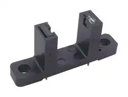
OPB815L
Transmissive Photo Interrupter, Phototransistor, Panel / Chassis, 9.5 mm, 1.52 mm, 20 mA, 2 V
⚠️ Reference pricing provided. In case of supply shortages, we will connect you with our trusted procurement partners to ensure your project's continuity.
- Manufacturer: TT ELECTRONICS / OPTEK TECHNOLOGY
- Product type: Transmissive Photo Interrupters
- Gap Width: 9.5mm
- Product Range: OPB815L Series
- Sensor Output: Phototransistor
- Aperture Width: 1.52mm
- Forward Voltage: 1.7V
- Sensor Mounting: Panel / Chassis
- Forward Current If: 20mA
- Reverse Voltage Vr: 2V
| Delivery and price | |
|---|---|
| Units per pack | 50 |
| Price | 2.1 € |
| Current stock | 10+ |
| Lead time | 23 days |
Datasheet

## **Deep Gap Slotted Switch with Wire and Connector Options** OPB815L, OPB815WZ Series

**==> picture [43 x 8] intentionally omitted <==**

**----- Start of picture text -----**<br>
L Package<br>**----- End of picture text -----**<br>


## Features:

- Wide slot width: 0.375” (9.5 mm)

- • Deep slot depth: 0.430” (10.9 mm)

**==> picture [51 x 9] intentionally omitted <==**

**----- Start of picture text -----**<br>
WZ Package<br>**----- End of picture text -----**<br>


## Description: The **OPB815**

This device can be ordered with PCBoard solderable leads (OPB815L) or with 26 AWG stranded, UL rated wire length of 24” [610 mm] (OPB815WZ).

|**Ordering Information**|**Ordering Information**|**Ordering Information**|**Ordering Information**|**Ordering Information**|**Ordering Information**|
|---|---|---|---|---|---|
|**Part**|**LED Peak**||**Slot**|**Aperture**<br>**Emitter /Sensor**|**Emitter /Sensor**<br>**Lead**<br>**Length /**|
|**OPB815L**|**890 nm**|**Transistor**|**0.375" / 0.430”**|**None**|**0.10" / 0.53"**|
|**OPB815WZ**|**890 nm**|**Transistor**|**0.375"/ 0.430”**|**None**|**24" / 26 AWG**|


## Applications:

- Non-contact object sensing

- Assembly line automation

- Machine automation

- Equipment security

- Machine safety

## **RoHS**

General Note

TT Electronics reserves the right to make changes in product specification without notice or liability.  All information is subject to TT Electronics’ own data and is considered accurate at time of going to print.

OPTEK Technology, Inc. 1645 Wallace Drive, Carrollton, TX 75006|Ph: +1 972 323 2200 www.optekinc.com | www.ttelectronics.com

Issue B      06/2016     Page 1

© TT electronics plc

## **Deep Gap Slotted Switch with Wire and Connector Options** OPB815L, OPB815WZ Series

**==> picture [118 x 59] intentionally omitted <==**

**----- Start of picture text -----**<br>
OPB815WZ<br>6,3540.25.250+.010i “— OPB815L<br>[ MILLIMETERS]<br>DIMENSIONS ARE IN:<br>INCHES<br>**----- End of picture text -----**<br>


|**Pin #**|**Description**|
|---|---|
|1|Anode|
|2|Cathode|
|3|Collector|
|4|Emitter|


|**Color**|**Description**|
|---|---|
|Red|Anode|
|Black|Cathode|
|White|Collector|
|Green|Emitter|


## ~~OO~~

OPTEK Technology, Inc. 1645 Wallace Drive, Carrollton, TX 75006|Ph: +1 972 323 2200 www.optekinc.com | www.ttelectronics.com

General Note TT Electronics reserves the right to make changes in product specification without notice or liability.  All information is subject to TT Electronics’ own data and is considered accurate at time of going to print.

Issue B      06/2016     Page 2

© TT electronics plc

## **Deep Gap Slotted Switch with Wire and Connector Options** OPB815L, OPB815WZ Series

Electrical Specifcations

Absolute Maximum Ratings (TA=25°C unless otherwise noted) ~~a~~ Storage & Operating Temperature Range -40° C to +80° C ~~ee~~ Lead Soldering Temperature [1/16 inch (1.6mm) from the case for 5 sec. with soldering iron] 260° C ~~ee~~ Input Infrared LED Continuous Forward Current 50 mA ~~ee~~ Reverse Voltage 2 V ~~a~~ Power Dissipation[(2)] 100 mW ~~ee~~ Output Phototransistor Collector-Emitter Voltage 30 V ~~ee~~ Emitter-Collector Voltage 5 V ~~es~~ Power Dissipation[(2)] 100 mW ~~ee~~ Electrical Characteristics (TA = 25°C unless otherwise noted) ~~a~~ SYMBOL PARAMETER MIN TYP MAX UNITS TEST CONDITIONS ~~aeeees ee es es~~ Input Infrared LED (see OP240 for additional information) ~~ee~~ VF Forward Voltage - - 1.7 V IF  = 20 mA ~~a es res ee es es~~ IR Reverse Current - - 100 μA VR  = 2 V ~~a ee ees ee ee es~~ Output Phototransistor (see OP550 for additional information) V(BR)CEO Collector-Emitter Breakdown Voltage 30 - - V IC = 1 mA ~~a es es ee ee es~~ V(BR)ECO Emitter-Collector Breakdown Voltage 5 - - v IE  = 100 μA ~~a ee es ee ee es~~ ICEO Collector-Emitter Dark Current - - 100 nA VCE  = 10 V, IF  = 0, EE  = 0 ~~a ee es ee ee ee~~ Coupled VCE(SAT) Collector-Emitter Saturation Voltage - - 0.4 V IC = 500 μA, IF  = 20 mA ~~eeee~~ IC(ON) On-State Collector Current 3.5 - 16 mA VCE  = 10 V, IF  = 20 mA ~~a ts ee es es ee es ee es es~~ Test Diagram Top to Bottom 0 Notes: (1) All wires are 26 AWG stranded, UL rated. ~~ye~~ (2) Derate linearly 1.67mW/°C above 25° C. (3) Methanol or isopropanol are recommended as cleaning agents.  The plastic housing is soluble in chlorinated hydrocarbons and keytones. (4) All parameters tested using pulse techniques. Emitter ~~||~~ Left to Right Right to Left Sensor 0 Width General Note OPTEK Technology, Inc. TT Electronics reserves the right to make changes in product specification without 1645 Wallace Drive, Carrollton, TX 75006|Ph: +1 972 323 2200 notice or liability.  All information is subject to TT Electronics’ own data and is www.optekinc.com | www.ttelectronics.com

TT Electronics reserves the right to make changes in product specification without notice or liability.  All information is subject to TT Electronics’ own data and is considered accurate at time of going to print.

Issue B      06/2016     Page 3

© TT electronics plc

## **Deep Gap Slotted Switch with Wire and Connector Options** OPB815L, OPB815WZ Series

## Performance

**==> picture [504 x 529] intentionally omitted <==**

**----- Start of picture text -----**<br>
OPB815 - Flag Next to Emitter OPB815 - Flag Next to Sensor<br>1.201.00 P| 1.201.00<br>fF | |<br>0.80 0.80<br>Left to Right<br>Left to Right Right to Left<br>Right to Left<br>0.60 0.60<br>TA) ae<br>Top to Bottom<br>0.40 0.40<br>Top to Bottom<br>0.200.00 fy Cn 0.200.00 ni a<br>0.00 0.05 0.10 0.15 0.20 0.25 0.00 0.05 0.10 0.15 0.20 0.25<br>Displacement Distance (inches) Displacement Distance (inches)<br>OPB815 - Flag in Middle of Slot Output Current vs Forward Current vs<br>1.2 Temperature<br>3<br>Normalized at IF  = 20mA at TA = 20°C, VCE = 10V<br>1.0<br>3<br>0.8<br>Left to Right 2<br>Right to Left<br>0.6<br>2<br>-40° C<br>0.4 Top to Bottom 1 -20° C<br>0° C<br>20° C<br>40° C<br>0.2 1<br>60° C<br>80° C<br>0.0 0<br>0.00 0.05 0.10 0.15 0.20 0.25 0 5 10 15 20 25 30 35 40 45 50<br>Displacement Distance (inches) Forward Current - mA<br> Response (mA)  Response (mA)<br>C(ON) C(ON)<br>Typical I Typical I<br> Response (mA)<br>C(ON)<br>Typical I Normalized Output Current<br>**----- End of picture text -----**<br>


Refer to Test Diagram on page 2 for definition of “Top to Bottom”, “Left to Right” and “Right to Left”

General Note

TT Electronics reserves the right to make changes in product specification without notice or liability.  All information is subject to TT Electronics’ own data and is considered accurate at time of going to print.

OPTEK Technology, Inc. 1645 Wallace Drive, Carrollton, TX 75006|Ph: +1 972 323 2200 www.optekinc.com | www.ttelectronics.com

Issue B      06/2016     Page 4

© TT electronics plc
Updated at February 9, 2023
About Novapart
Novapart is a B2B electronic component broker specialising in stock shortages and cost reduction. We source hard-to-find parts and identify compliant alternatives across a catalogue of 420,000+ components from 500+ manufacturers.
Learn more →Stock Shortage Specialist
When a component is unavailable, discontinued or has an unacceptable lead time, we tap into our network of vetted European and Asian distributors to source what you need — without compromising on quality or traceability.
Request a quote →Compliant Alternatives
We identify pin-to-pin, electrically equivalent substitutes that meet the same certifications (RoHS, AEC-Q100, REACH) as your original specification — validated against datasheets, not just part numbers. Often at a lower cost.
BOM Analysis service →