
Image not available
Illustrative purposes only

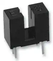
OPB666N
Transmissive Photo Interrupter, Open Collector, Through Hole, 3.18 mm, 1.27 mm, 50 mA, 3 V
⚠️ Reference pricing provided. In case of supply shortages, we will connect you with our trusted procurement partners to ensure your project's continuity.
- Manufacturer: TT ELECTRONICS / OPTEK TECHNOLOGY
- Product type: Transmissive Photo Interrupters
- Gap Width: 3.18mm
- Sensor Output: Open Collector
- Aperture Width: 1.27mm
- Forward Voltage: 1.6V
- Sensor Mounting: Through Hole
- Forward Current If: 50mA
- Reverse Voltage Vr: 3V
| Delivery and price | |
|---|---|
| Units per pack | 50 |
| Price | 3.63 € |
| Current stock | 10+ |
| Lead time | 30 days |
Datasheet

- - - - |**Ordering Information**<br>~~§[_——OOO—SOSOOCCSCTCC~SCSY~~|**Ordering Information**<br>~~§[_——OOO—SOSOOCCSCTCC~SCSY~~|**Ordering Information**<br>~~§[_——OOO—SOSOOCCSCTCC~SCSY~~|**Ordering Information**<br>~~§[_——OOO—SOSOOCCSCTCC~SCSY~~|**Ordering Information**<br>~~§[_——OOO—SOSOOCCSCTCC~SCSY~~|**Ordering Information**<br>~~§[_——OOO—SOSOOCCSCTCC~SCSY~~| |---|---|---|---|---|---| |**Part**<br>**Number**|**Package**<br>**Style**|**Sensor**<br>**Photologic®**|**Aperture**<br>**Emitter /**<br>**Sensor**|**Slot Width /**<br>**Depth**|**Slot Width /**<br>**Lead Length /**<br>**Spacing**| |OPB615|N|10K Pull-up|None<br>en Collector|0.150" /<br>0.240”|0.100" (min) /<br>0.275"| |OPB616||Open Collector|||| |OPB617||Inv-10K Pull-up|||| |OPB618||Inv-Open Collector|||| |OPB625||10K Pull-up|None<br>en Collector|0.190" /<br>0.285”|0.100" (min) /<br>0.320"| |OPB626||Open Collector|||| |OPB627||Inv-10K Pull-up|||| |OPB628||Inv-Open Collector|||| |OPB665N||10K Pull-up|0.05”/ 0.01”<br>en Collector<br>en Collector|0.125" /<br>0.345”|| |OPB666N||Open Collector|||| |OPB667N||Inv-10K Pull-Up|||| |OPB668N||Inv-Open Collector|||| |OPB665T|T|10K Pull-up|||| |OPB666T||Open Collector|||| |OPB667T||Inv-10K Pull-up|||| |OPB668T||Inv-Open Collector|||| **==> picture [24 x 7] intentionally omitted <==** **----- Start of picture text -----**<br> RoHS<br>**----- End of picture text -----**<br> **OPB615/625/665N Buffered 10K Pull-Up** **OPB 616/** ~~**6**~~ **26/** ~~**6**~~ **66N Buffered Open-Collector** **OPB615, OPB616, OPB617, OPB618** |**Pin Color/**|| |---|---| |**Number**<br>1|**Description**<br>Anode| |2|Cathode| |3|Vcc| |4<br>5|Output<br>Ground| **==> picture [115 x 18] intentionally omitted <==** **----- Start of picture text -----**<br> [ MILLIMETERS]<br>DIMENSIONS ARE IN:<br>INCHES<br>**----- End of picture text -----**<br> ## **OPB625, OPB626, OPB627, OPB628** |**Pin Color/**<br>**Number**|**Description**| |---|---| |1|Anode| |2|Cathode| |3|Vcc| |4|Output| |5|Ground| ## **OPB665, OPB666, OPB667, OPB668 (N and T)** **==> picture [115 x 18] intentionally omitted <==** **----- Start of picture text -----**<br> [ MILLIMETERS]<br>DIMENSIONS ARE IN:<br>INCHES<br>**----- End of picture text -----**<br> **==> picture [105 x 90] intentionally omitted <==** **----- Start of picture text -----**<br> Pin Color/<br>Number Description<br>1 Anode<br>2 Cathode<br>3 Vcc<br>4 Output<br>5 Ground<br>**----- End of picture text -----**<br> |OPB625, OPB626, OPB627, OPB628 Series<br>~~OPB665, OPB666, OPB667, OPB668 (N and T Series)~~|OPB625, OPB626, OPB627, OPB628 Series<br>~~OPB665, OPB666, OPB667, OPB668 (N and T Series)~~| |---|---| ||| |Storage & Operating Temperature Range|-40° C to +100° C| |Lead Soldering Temperature (1/16 inch (1.6mm) from the case for 5 sec. with soldering iron)(1)|260° C| ||| |Forward DC Current|50 mA| |Peak Forward Current (1 μs pulse width, 300 pps)|3 A| |Reverse DC Voltage|3 V| |Power Dissipation(2)|100 mW| |~~a~~|~~a~~| |Supply Voltage, VCC|18 V| |Duration of Output Short to VCC|1 second| |Voltage at Output(5)|Vcc| |Low Level Output Current (sinking)|16 mA| |Power Dissipation(3)|240° mW| Notes: (1) RMA flux is recommended. Duration can be extended to 10 seconds maximum when flow soldering. (2) Derate linearly 1.33 mW/° C above 25° C. (3) Derate linearly 2.50 mW/° C above 25° C. (4) Normal application would be with light source blocked, simulated by IF = 0 mA. (5) Open Collector devices = 30 volts |VF|Forward Voltage||-|-|1.6|V|IF= 10 mA| |---|---|---|---|---|---|---|---| |IR|Reverse Current||-|-|100|μA|VR= 3 V| ||||||||| |VCC|Operating DC Supply Voltage|Operating DC Supply Voltage|4.5|-|16|V|| ||LED Positive-Going|OPB615-618|0.1|0.55|3||| |IF(+)|Threshold Current|OPB625-628|0.1|0.6|3|mA|VCC= 5 V| |||OPB665-668|0.1|1.6|10||| |IF(+)/IF(-)|Hysteresis||1.05|1.20|1.90||VCC= 5 V| |OPB625, OPB626, OPB627, OPB628 Series<br>~~OPB665,OPB666,OPB667,OPB668(NandTSeries)~~|OPB625, OPB626, OPB627, OPB628 Series<br>~~OPB665,OPB666,OPB667,OPB668(NandTSeries)~~|OPB625, OPB626, OPB627, OPB628 Series<br>~~OPB665,OPB666,OPB667,OPB668(NandTSeries)~~|OPB625, OPB626, OPB627, OPB628 Series<br>~~OPB665,OPB666,OPB667,OPB668(NandTSeries)~~|OPB625, OPB626, OPB627, OPB628 Series<br>~~OPB665,OPB666,OPB667,OPB668(NandTSeries)~~|OPB625, OPB626, OPB627, OPB628 Series<br>~~OPB665,OPB666,OPB667,OPB668(NandTSeries)~~|OPB625, OPB626, OPB627, OPB628 Series<br>~~OPB665,OPB666,OPB667,OPB668(NandTSeries)~~| |---|---|---|---|---|---|---| |~~OPB665, OPB666, OPB667, OPB668 (N and T Series)~~<br>~~“smmeot|~~<br>~~panaweren~~<br>~~|IN|TYP|ax[UNITS|TESTCONDITIONS~~||||||| |~~“smmeot|~~|~~|~~<br>~~panaweren~~<br>~~|~~|~~|IN|~~|~~IN|TYP|~~|~~|ax[UNITS~~|~~[UNITS|~~|~~|TESTCONDITIONS~~| |~~“smmeot|~~<br>~~panaweren~~<br>~~| IN| TYP | ax [UNITS| TESTCONDITIONS~~||||||| |ICCH|High Level Supply Current:<br>Buffer, 10k Pull-up<br>OPB615, 625, 665<br>Buffer, Open-Collector<br>OPB616, 626, 666|-<br>-|5<br>5|12<br>12|mA|NO LOAD on Output(3)| ||Inverted, 10k Pull-up<br>OPB617, 627, 667<br>Inverted, Open-Collector<br>OPB618, 628, 668|-<br>-|4<br>4|12<br>12|mA|NO LOAD on Output<br>IF= 0 mA| |ICCL|Low Level Supply Current:<br>Buffer, 10k Pull-up<br>OPB615, 625, 665<br>Buffer, Open-Collector<br>OPB616, 626, 666|-<br>-|5.5<br>4.0|12<br>12|mA|NO LOAD on Output<br>IF= 0 mA| ||Inverted, 10k Pull-up<br>OPB617, 627, 667<br>Inverted, Open-Collector<br>OPB618, 628, 668|-<br>-|6.5<br>5.0|12<br>12|mA|NO LOAD on Output(3)| |VOH|High Level Output Voltage:<br>Buffer, 10k Pull-up<br>OPB615, 625, 665<br>Buffer, Open-Collector<br>OPB616, 626, 666|VCC-<br>1.5|-<br>-|-<br>-|V|IOH= 100 µA(3)| ||Inverter, 10k Pull-up<br>OPB617, 627, 667<br>Inverter, Open-Collector<br>OPB618, 628, 668|VCC-<br>1.5|-<br>-|-<br>-|V|IOH= 100 µA(1)<br>IF= 0 mA| |IOH|High Level Output Voltage:<br>Buffer, Open-Collector<br>OPB616, 626, 666|-|-|100|µA|VOH= 30 V(3)| ||Inverter, Open-Collector<br>OPB618, 628, 668|-|-|100|µA|IF= 0 mA, VOH= 30 V(1)| |VOL|Low Level Output Voltage:<br>Buffer, 10k Pull-up<br>OPB615, 625, 665<br>Buffer, Open-Collector<br>OPB616, 626, 666|-|-|0.4|V|IOL= 16 mA, Vcc = 4.5 V(3)(1)| ||Inverter, 10k Pull-up<br>OPB617, 627, 667<br>Inverter, Open-Collector<br>OPB618, 628, 668|-|-|0.4|V|IOL= 16 mA, IF= 0 mA| |tr, tf|Output Rise Time, Output Fall Time||30||ns|f = 10 kHz,<br>RL= 300 Ω, DC = 50%(3)| |tPLH|Propagation Delay, Low-High<br>Buffer, 10k Pull-up<br>OPB615, 625, 665<br>Buffer, Open-collector<br>OPB616, 626, 666||0.6||µs|| ||Inverter, 10k Pull-up<br>OPB617, 627, 667<br>Inverter, Open-Collector<br>OPB618, 628, 668||3.0||µs|| |tPHL|Propagation Delay, High-Low<br>Buffer, 10k Pull-up<br>OPB615, 625, 665<br>Buffer, Open-collector<br>OPB616, 626, 666||3.0||µs|| ||Inverter, 10k Pull-up<br>OPB617, 627, 667<br>Inverter, Open-Collector<br>OPB618, 628, 668||0.6||µs|| |Data Rate||-|100|-|kHz|RL= 300 Ω, DC = 50%(4)| |~~a~~||||||| **OPB615 - Flag next to Emitter** **OPB615 - Flag next to Sensor** **==> picture [504 x 522] intentionally omitted <==** **----- Start of picture text -----**<br> 1.20 1.20<br>1.00 1.00<br>Right to Left Right to Left<br>Back Back<br>0.80 reeae ee 0.80 ei Top to Bottom<br>Top to Bottom<br>Right to Left Right to Left<br>0.60 ee| eee ee 0.60 ool ff et e e ee<br>Bottom<br>to Top<br>Bottom<br>to Top<br>0.40 0.40<br>Left to Right Left to Right<br>Back Back<br>Left to Right Left to Right<br>0.20 foio 0.20 re<br>0.00 0.00<br>0.000'' 0.050'' 0.100'' 0.150'' 0.200'' 0.250'' 0.000'' 0.050'' 0.100'' 0.150'' 0.200'' 0.250''<br>Displacement(inches) Displacement(inches)<br>OPB615 - Flag in Middle of Slot<br>1.20<br>1.00<br>Top to Bottom<br>0<br>Right to Left<br>Back<br>0.80<br>TE Top to Bottom ot<br>Right to Left<br>0.60 ise|<br>Bottom<br>to Top Emitter<br>0.40 TE : | Left to Right > Left to Right =<“— Right to Left<br>Back Sensor<br>Left to Right<br>0.20 pa _<br>0 Width<br>0.00<br>0.000'' 0.050'' 0.100'' 0.150'' 0.200'' 0.250''<br>Displacement(inches)<br>Logic<br>Logic<br>Logic<br>**----- End of picture text -----**<br> **==> picture [133 x 10] intentionally omitted <==** **----- Start of picture text -----**<br> OPB625 - Flag Next to Emitter<br>**----- End of picture text -----**<br> **==> picture [132 x 10] intentionally omitted <==** **----- Start of picture text -----**<br> OPB625 - Flag Next to Sensor<br>**----- End of picture text -----**<br> **==> picture [504 x 531] intentionally omitted <==** **----- Start of picture text -----**<br> 1.2 1.2<br>1 1<br>Right to Left Right to Left<br>Back Back<br>0.8 ore PE 0.8<br>Top to Bottom Top to Bottom<br>Right to Left Right to Left<br>0.6 0.6<br>Bottom Bottom<br>to Top to Top<br>0.4 0.4<br>Left to Right Left to Right<br>Left to Right Back Left to Right Back<br>0.2 0.2<br>0 0<br>0.00 0.05 0.10 0.15 0.20 0.25 0.00 0.05 0.10 0.15 0.20 0.25<br>Displacement Distance (inches) Displacement Distance (inches)<br>OPB625 - Flag in Middle of Slot<br>1.20<br>1.00 0 Top to Bottom<br>Right to Left<br>Back<br>0.80 ott<br>Top to Bottom<br>Right to Left<br>0.60 Pde]r | ft Emitter<br>Bottom<br>to Top<br>Left to Right Right to Left<br>0.40 ele<br>Sensor<br>Left to Right<br>Back<br>Left to Right<br>0 Width<br>0.20 ane<br>0.00<br>0.00 0.05 0.10 0.15 0.20 0.25<br>Displacement Distance (inches)<br>Logic<br>Logic<br>Logic<br>**----- End of picture text -----**<br> **==> picture [504 x 543] intentionally omitted <==** **----- Start of picture text -----**<br> OPB665 - Flag next to Emitter OPB665 - Flag next to Sensor<br>1.20 1.20<br>1. 00 1.00<br>Right to Left Right to Left<br>Back Back<br>0.80 a Ee 0.80 eee eee<br>Right to Left Right to Left<br>Top to Bottom Top to Bottom<br>0.60 ecmc 0.60 ees-<br>Bottom Bottom<br>to Top to Top<br>0.40 ee| 0.40 it | Ce<br>Left to Right Left to Right<br>Left to Right Back Left to Right | Back<br>0.20 oi 0.20 i:<br>0.00 oe fe 0.00<br>0.000'' 0.050'' 0.100'' 0.150'' 0.200'' 0.250'' 0.000'' 0.050'' 0.100'' 0.150'' 0.200'' 0.250''<br>Displacement(inches) Displacement(inches)<br>OPB665 - Flag in Middle of Slot<br>1.20<br>Top to Bottom<br>0<br>1.00<br>Right to Left<br>Back<br>0.80 cle<br>Right to Left<br>ay ‘<br>Top to Bottom<br>0.60 es ce Emitter<br>Bottom<br>to Top Left to Right Right to Left<br>0.40 ee<br>Sensor<br>Left to Right<br>Left to Right Back<br>0 Width<br>0.20 ee. ne —<br>i<br>0.00<br>0.000'' 0.050'' 0.100'' 0.150'' 0.200'' 0.250''<br>Displacement(inches)<br>Logic<br>Logic Logic<br>**----- End of picture text -----**<br>
Updated at February 9, 2023
About Novapart
Novapart is a B2B electronic component broker specialising in stock shortages and cost reduction. We source hard-to-find parts and identify compliant alternatives across a catalogue of 420,000+ components from 500+ manufacturers.
Learn more →Stock Shortage Specialist
When a component is unavailable, discontinued or has an unacceptable lead time, we tap into our network of vetted European and Asian distributors to source what you need — without compromising on quality or traceability.
Request a quote →Compliant Alternatives
We identify pin-to-pin, electrically equivalent substitutes that meet the same certifications (RoHS, AEC-Q100, REACH) as your original specification — validated against datasheets, not just part numbers. Often at a lower cost.
BOM Analysis service →