
Image not available
Illustrative purposes only

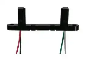
OPB315WZ
PHOTOTRANSISTOR SENSOR, 850NM
⚠️ Reference pricing provided. In case of supply shortages, we will connect you with our trusted procurement partners to ensure your project's continuity.
- Manufacturer: TT ELECTRONICS / OPTEK TECHNOLOGY
- Product type: Optical / Slot Photoelectric Sensors
- Product Range: OPB315 Series
- Sensor Output: Phototransistor
| Delivery and price | |
|---|---|
| Units per pack | 250 |
| Price | 5.5 € |
| Current stock | 100+ |
| Lead time | 7 days |
Datasheet

**==> picture [36 x 7] intentionally omitted <==** **----- Start of picture text -----**<br> OPB315L<br>**----- End of picture text -----**<br> - Lateral package - Opaque black plastic **==> picture [45 x 7] intentionally omitted <==** **----- Start of picture text -----**<br> OPB315WZ<br>**----- End of picture text -----**<br> - 850 nm wavelength - Choice of leads or wires Each slotted optical switch in this series consists of an infrared emitting diode (LED) and a NPN silicon phototransistor mounted on opposite sides of a 0.90” (22.9 mm) wide slot in an opaque black plastic package. The **OPB315L** has 0.25” minimum leads, while the **OPB315WZ** has a minimum of 24” (610 mm) 26 AWG wires. Phototransistor switching takes place whenever an opaque object passes through the slot. **==> picture [507 x 372] intentionally omitted <==** **----- Start of picture text -----**<br> Ordering Information<br>Part LED Peak Slot Width / Aperture Wire or Lead<br> Non-contact object sensing Number Wavelength Sensor Depth Emitter / Sensor Length / Gage<br> Assembly line automation<br>OPB315L 0.25” / N/A<br> Machine automation<br> 850 nm Transistor 0.90"/0.46” 0.03” R / 0.03” R<br> Equipment security OPB315WZ 24” min/<br>26 AWG wires<br>_ Machine safety T=<br>OPB315L<br>SYMBOLIZATION LA [47.63]<br>SYMBOLIZEFOR ANODEWHITE DOT CS]) [a| 2>cS)j Qt }re-—:41.281.62587sS78)= [3.18]125<br>[3.18]<br>2X 0.125<br>OPB315L<br>1 3 [25.40]<br>° e [2.0340.13] 1.000 OPTICAL ¢ [6.35]<br>.080+.005 [22.86] 250<br>Vv -900<br>Vv PN _ _ [14.86<br>a 585 ]<br>e e Tt<br>2 4 Cc3.18J AX .25[6.35] MIN.<br>125 — Pes) Fg)[2.54] ie<br>Pin # LED Pin # Transistor _ White Dot<br>1 2 Cathode Anode 3 4 Collector Emitter © Ff = 4 ©)<br>— NOTES: PINPIN 12 PIN 3<br>1. TOLERANCES ARE ± 0.010 [0.254] UNLESS<br>OTHERWISE SPECIFIED.<br>5 DIMENSIONS ARE IN: [MILLIMETERS] CATHODE OTER<br>RoHS INCHES<br>**----- End of picture text -----**<br> **==> picture [48 x 8] intentionally omitted <==** **----- Start of picture text -----**<br> OPB315WZ<br>**----- End of picture text -----**<br> NOTES: **==> picture [110 x 31] intentionally omitted <==** **----- Start of picture text -----**<br> 1. TOLERANCES ARE ± 0.010 UNLESS<br>OTHERWISE SPECIFIED.<br>DIMENSIONS ARE IN: [MILLIMETERS]<br>INCHES<br>**----- End of picture text -----**<br> **==> picture [76 x 102] intentionally omitted <==** **----- Start of picture text -----**<br> OPB315WZ<br>Red White<br>e e<br>V ir,<br>e e<br>Black Green<br>**----- End of picture text -----**<br> |**Pin #/**<br>**Color**|**LED**|**Pin #/**<br>**Color**|**Transistor**| |---|---|---|---| |Black|Cathode|White|Collector| |Red|Anode|Green|Emitter| |Electrical Specifications|Electrical Specifications| |---|---| |Absolute Maximum Ratings (T,= 25°C unlessotherwise noted)|| |Storage Temperature Range|-40oC to +80oC| |Operating Temperature Range|-40oC to +80oC| |Reverse Voltage|2.0 V| |Continuous Forward Current|50 mA| |Peak Forward Current [measured at 1 µs pulse width and 300 pps]|1.0 A| |Lead Soldering Temperature [1/16 inch (1.6 mm) from case for 5 seconds with soldering iron]|260° C(1)(2)| |Power Dissipation (Input Diode)|100 mW| |Power Dissipation (Output Phototransistor)|100 mW| |Electrical Characteristics (T,= 25° C unless otherwise noted)<br>~~SYMBOL~~<br>~~PARAMETER~~<br>~~/MIN|TYP|MAX|UNITS~~<br>~~TESTCONDITIONS~~|Electrical Characteristics (T,= 25° C unless otherwise noted)<br>~~SYMBOL~~<br>~~PARAMETER~~<br>~~/MIN|TYP|MAX|UNITS~~<br>~~TESTCONDITIONS~~|Electrical Characteristics (T,= 25° C unless otherwise noted)<br>~~SYMBOL~~<br>~~PARAMETER~~<br>~~/MIN|TYP|MAX|UNITS~~<br>~~TESTCONDITIONS~~|Electrical Characteristics (T,= 25° C unless otherwise noted)<br>~~SYMBOL~~<br>~~PARAMETER~~<br>~~/MIN|TYP|MAX|UNITS~~<br>~~TESTCONDITIONS~~|Electrical Characteristics (T,= 25° C unless otherwise noted)<br>~~SYMBOL~~<br>~~PARAMETER~~<br>~~/MIN|TYP|MAX|UNITS~~<br>~~TESTCONDITIONS~~|Electrical Characteristics (T,= 25° C unless otherwise noted)<br>~~SYMBOL~~<br>~~PARAMETER~~<br>~~/MIN|TYP|MAX|UNITS~~<br>~~TESTCONDITIONS~~|Electrical Characteristics (T,= 25° C unless otherwise noted)<br>~~SYMBOL~~<br>~~PARAMETER~~<br>~~/MIN|TYP|MAX|UNITS~~<br>~~TESTCONDITIONS~~| |---|---|---|---|---|---|---| |~~SYMBOL~~|~~PARAMETER~~<br>~~/MIN~~|~~/MIN|~~|~~|TYP|~~|~~|MAX|~~|~~|UNITS~~|~~TESTCONDITIONS~~| |**Input Diode**<br>~~SYMBOL~~<br>~~PARAMETER~~<br>~~/MIN | TYP | MAX | UNITS~~<br>~~TEST CONDITIONS~~||||||| |VF|Forward Voltage|-|1.4|1.7|V|IF= 20 mA| |IR|Reverse Current|-|-|100|µA|VR= 2 V| |**Output Phototransistor**(see OP550 for additional information)||||||| |V(BR)(CEO)|Collector-Emitter Breakdown Voltage|30|-|-|V|ICE= 100 µA, IF= 0 mA| |V(BR)(ECO)|Emitter-Collector Breakdown Voltage|5.0|-|-|V|IEC= 100 µA, IF= 0 mA, EE= 0| |ICEO|Collector-Emitter Leakage Current|-|-|100|nA|VCE= 10.0 V, IF= 0 mA, EE= 0| |**Coupled**||||||| |IC(ON)|On-State Collector Current|0.5|1.0|-|mA|VCE= 0.4 V, IF= 20 mA| |VCE(SAT)|Collector-Emitter|-|-|0.4|V|IC= 500 µA, IF= 20 mA| Notes: 1. RMA flux is recommended. Duration can be extended to 10 seconds maximum when flow soldering. 2. Derate linearly 1.33 mW/° C above 25° C. ## **OPB315** **==> picture [499 x 553] intentionally omitted <==** **----- Start of picture text -----**<br> Forward Voltage vs Forward Current vs<br>Temperature Optical Power vs Forward Current vs<br>Temperature<br>1.8 4.0<br>-60° C<br>-40° C Normalized at IF = 20 mA, TA = 20°C<br>3.5 -20° C<br>1.6 0° C<br>20° C<br>40° C<br>3.0<br>—SS = 60° C TT,<br>1.4 80° C<br>100° C<br>a 2.5 OE<br>1.2 gern 2.0<br>cae LEE<br>-60° C<br>-40° C 1.5<br>1.0 -20° C<br>aa ny Zo<br>0° C<br>20° C 1.0<br>40° C<br>0.8 PTT TT 60° C en 22<br>80° C<br>100° C 0.5<br>120° C<br>0.6 0.0 > si<br>0 5 10 15 20 25 30 35 40 45 50 0 10 20 30 40 50<br>Forward Current (mA) Forward Current IF (mA)<br>OPB315 - Flag Next to Emitter OPB315 - Flag Next to Sensor<br>1.2 1.2<br>Top to Bottom<br>Top to Bottom<br>1.0 1.0<br>0.8 0.8<br>Bawanneven<br>\<br>0.6 0.6<br>Left to Right Right to Left<br>Left to Right Right to Left<br>0.4 A 0.4 i. f\<br>\<br>\<br>0.20.0 OAMAM—— = 0.20.0 J h -—<br>0.00 0.05 0.10 0.15 0.20 0.25 0.00 0.05 0.10 0.15 0.20 0.25<br>Displacement Distance (inches) Displacement Distance (inches)<br> Response<br>C(ON)<br>Normalized I<br> Response<br>C(ON)<br>Normalized I<br>Relative Output Power<br>Typical Forward Voltage (V)<br>**----- End of picture text -----**<br>
Updated at February 9, 2023
About Novapart
Novapart is a B2B electronic component broker specialising in stock shortages and cost reduction. We source hard-to-find parts and identify compliant alternatives across a catalogue of 420,000+ components from 500+ manufacturers.
Learn more →Stock Shortage Specialist
When a component is unavailable, discontinued or has an unacceptable lead time, we tap into our network of vetted European and Asian distributors to source what you need — without compromising on quality or traceability.
Request a quote →Compliant Alternatives
We identify pin-to-pin, electrically equivalent substitutes that meet the same certifications (RoHS, AEC-Q100, REACH) as your original specification — validated against datasheets, not just part numbers. Often at a lower cost.
BOM Analysis service →