
Image not available
Illustrative purposes only

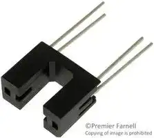
OPB200
OPTICAL SWITCH, 5.1MM, PHOTOTRANSISTOR
⚠️ Reference pricing provided. In case of supply shortages, we will connect you with our trusted procurement partners to ensure your project's continuity.
- Manufacturer: TT ELECTRONICS / OPTEK TECHNOLOGY
- Product type: Transmissive Photo Interrupters
- Gap Width: 5.08mm
- Sensor Output: Phototransistor
- Aperture Width: 1.52mm
- Forward Voltage: 1.7V
- Sensor Mounting: Through Hole
- Forward Current If: 50mA
- Reverse Voltage Vr: 2V
| Delivery and price | |
|---|---|
| Units per pack | 500 |
| Price | 1.3 € |
| Current stock | 10+ |
| Lead time | 14 days |
Datasheet

- Features: - Housing material Opaque to visible and infrared light - Non–contact switching - Printed PCBoard mount - 0.200” (5.1 mm) slot width, 0.320” (8.1 mm) slot depth The **OPB200** contains an Infrared LED (890 nm) and a Phototransistor paired in a plastic housing. The housing is an opaque grade of injection-molded plastic, which minimizes the assembly’s sensitivity to visible and nearinfrared radiation. Each device has approximately 0.060” [1.52 mm] diameter lenses providing the versatility necessary for general switching applications. The output Phototransistor ON state conducts current (IC(ON)) when no object is in the slot. The output switches to the OFF state when a device interrupts the light beam from the Emitter (LED) to the Phototransistor. The Phototransistor can acknowledge light between 400 nm and 1100 nm with optimum response in the 880 nm range. Custom electrical, wire and cabling and connectors are available. Contact your local representative or OPTEK for more information. **==> picture [484 x 217] intentionally omitted <==** **----- Start of picture text -----**<br> Non-contact interruptive object sensing 1 4<br> Assembly line automation e e<br> Machine automation<br>oe / »<br> Equipment security [12.95+0.25| Vv vy<br> Machine safety [2.03+0.25 ] 9102.01<br>[2.03+0.25.080+.01 [5.08+0.25.200+.01 ] ° °<br>2 3<br>.080+.01 ] T 1 :<br>Pin # Description 400+.01<br>[8.9] 10.16#0.25<br>1 Anode MIN +<br>2 Cathode OPTICAL ¢<br>3 Collector<br>4 Emitter a AIP 4x [0.51]020 sa. TYP<br>[10.16+0.25|<br>[2.54+0.25 | 4004.01 [6.10+0.25<br>1004.01 2 3 .240+.01 ]<br>[ MILLIMETERS]<br>] 4 DIMENSIONS ARE IN:<br>INCHES<br>**----- End of picture text -----**<br> ## **Ordering Information** ||**Part**<br>**Number**|**LED Peak**<br>**Wavelength**|**Sensor**|**Slot Width /**<br>**Depth**|**Aperture**<br>**Emitter/Sensor**|**Lead Length /**<br>**Spacing**|| |---|---|---|---|---|---|---|---| |**RoHS**|OPB200|890 nm|Transistor|0.200”/0.320”|None|0.425”/0.400|0.400| |Absolute Maximum Ratings (T,= 25°C unlessotherwise noted)|Absolute Maximum Ratings (T,= 25°C unlessotherwise noted)| |---|---| |Storage & Operating Temperature Range|-40°C to +85°C| |Lead Soldering Temperature [1/16 inch (1.6mm) from the case for 5 sec. with soldering iron](1)|260°C| |**Input Diode**|| |Forward DC Current|50 mA| |Peak Forward Current (1 μs pulse width, 300 pps)|3 A| |Reverse DC Voltage|2 V| |Power Dissipation(2)|100 mW| |**Output Phototransistor**|| |Collector-Emitter Voltage|30 V| |Emitter-Collector Voltage|5 V| |Collector DC Current|30 mA| |Power Dissipation(2)|100 mW| |Electrical Characteristics (T,= 25° C unless otherwise noted)<br>~~SYMBOL~~<br>~~PARAMETER~~<br>~~|MIN|TYP|MAX|UNITS~~<br>~~TESTCONDITIONS~~|Electrical Characteristics (T,= 25° C unless otherwise noted)<br>~~SYMBOL~~<br>~~PARAMETER~~<br>~~|MIN|TYP|MAX|UNITS~~<br>~~TESTCONDITIONS~~|Electrical Characteristics (T,= 25° C unless otherwise noted)<br>~~SYMBOL~~<br>~~PARAMETER~~<br>~~|MIN|TYP|MAX|UNITS~~<br>~~TESTCONDITIONS~~|Electrical Characteristics (T,= 25° C unless otherwise noted)<br>~~SYMBOL~~<br>~~PARAMETER~~<br>~~|MIN|TYP|MAX|UNITS~~<br>~~TESTCONDITIONS~~|Electrical Characteristics (T,= 25° C unless otherwise noted)<br>~~SYMBOL~~<br>~~PARAMETER~~<br>~~|MIN|TYP|MAX|UNITS~~<br>~~TESTCONDITIONS~~|Electrical Characteristics (T,= 25° C unless otherwise noted)<br>~~SYMBOL~~<br>~~PARAMETER~~<br>~~|MIN|TYP|MAX|UNITS~~<br>~~TESTCONDITIONS~~|Electrical Characteristics (T,= 25° C unless otherwise noted)<br>~~SYMBOL~~<br>~~PARAMETER~~<br>~~|MIN|TYP|MAX|UNITS~~<br>~~TESTCONDITIONS~~| |---|---|---|---|---|---|---| |~~SYMBOL~~|~~PARAMETER~~<br>~~|~~|~~|MIN|~~|~~|TYP|~~|~~|MAX|~~|~~|UNITS~~|~~TESTCONDITIONS~~| |**Input Diode**(see OP140 for additional information)<br>~~SYMBOL~~<br>~~PARAMETER~~<br>~~| MIN | TYP | MAX | UNITS~~<br>~~TEST CONDITIONS~~||||||| |VF|Forward Voltage|-|-|1.7|V|IF= 20 mA| |IR|Reverse Current|-|-|100|µA|VR= 2 V| |**Output Phototransistor**(see OP550 for additional information)||||||| |V(BR)CEO|Collector-Emitter Breakdown Voltage|30|-|-|V|IC= 1 mA| |V(BR)ECO|Emitter-Collector Breakdown Voltage|5|-|-|V|IE= 100 µA| |ICEO|Collector Dark Current|-|-|100|nA|VCE= 10 V, IF= 0, EE= 0| |**Combined**||||||| |VCE(SAT)|Collector-Emitter Saturation Voltage|-|-|0.4|V|IC= 100 µA, IF= 20 mA| |IC(ON)|On-State Collector Current|1|4|6|mA|VCE= 0.4 V, IF= 20 mA| Notes: (1) RMA flux is recommended. Duration can be extended to 10 seconds maximum when flow soldering. (2) Derate linearly 1.67 mW/°C above 25 ° C. (3) All parameters tested using pulse techniques. (4) Lead spacing of 0.400” (10.16 mm). Leads are a minimum of 0.020” sq. (0.508 mm) and 0.425” (10.795 mm) long. (5) Methanol or isopropanol are recommended as cleaning agents. Plastic housing is soluble in chlorinated hydrocarbons and ketones. (6) Polarity is denoted by a notch next to pin 1 (LED Anode) of the package. **==> picture [116 x 10] intentionally omitted <==** **----- Start of picture text -----**<br> OPB200 - Flag Next to Emitter<br>**----- End of picture text -----**<br> **==> picture [116 x 9] intentionally omitted <==** **----- Start of picture text -----**<br> OPB200 - Flag Next to Sensor<br>**----- End of picture text -----**<br> **==> picture [514 x 550] intentionally omitted <==** **----- Start of picture text -----**<br> 1.20 1.20<br>1.00 1.00<br>\ \<br>\<br>0.80 \ 0.80 \ \<br>\<br>\ \<br>0.60 0.60<br>0.40 0.40<br>Right to Left Right to Left<br>0.20 Left to Right 0.20 Left to Right<br>Top to Bottom Top to Bottom<br>0.00 0.00<br>0.00 0.05 0.10 0.15 0.20 0.25 0.00 0.05 0.10 0.15 0.20 0.25<br>Displacement Distance (inches) Displacement Distance (inches)<br>OPB200 - Flag in Middle of Slot<br>1.20<br>Top to Bottom<br>0<br>1.00<br>\\ v<br>\<br>0.80<br>\<br>\<br>0.60 \ Emitter<br>||<br>Left to Right Right to Left<br>\ ——__> <——<br>0.40 |<br>Sensor<br>Right to Left<br>0 Width<br>0.20 Left to Right<br>Top to Bottom<br>0.00 ee ce<br>0.00 0.05 0.10 0.15 0.20 0.25<br>Displacement Distance (inches)<br>Response (mA)<br>C(ON)<br>Typical I<br> Response (mA)<br>C(ON)<br>Typical I<br> Response (mA)<br>C(ON)<br>Typical I<br>**----- End of picture text -----**<br>
Updated at February 9, 2023
About Novapart
Novapart is a B2B electronic component broker specialising in stock shortages and cost reduction. We source hard-to-find parts and identify compliant alternatives across a catalogue of 420,000+ components from 500+ manufacturers.
Learn more →Stock Shortage Specialist
When a component is unavailable, discontinued or has an unacceptable lead time, we tap into our network of vetted European and Asian distributors to source what you need — without compromising on quality or traceability.
Request a quote →Compliant Alternatives
We identify pin-to-pin, electrically equivalent substitutes that meet the same certifications (RoHS, AEC-Q100, REACH) as your original specification — validated against datasheets, not just part numbers. Often at a lower cost.
BOM Analysis service →