
Image not available
Illustrative purposes only

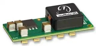
OKY2-T/16-D12N-C
Non Isolated POL DC/DC Converter, Programmable, ITE, 80 W, 752.5 mV, 5.5 V, 16 A, Adjustable
⚠️ Reference pricing provided. In case of supply shortages, we will connect you with our trusted procurement partners to ensure your project's continuity.
- Manufacturer: MURATA POWER SOLUTIONS
- Product type: DC / DC Non Isolated Board Mount Converters - Adjustable Output
- Output Power Max:80W; Output Voltage Min:752.5mV; Output Voltage Max:5.5V; Output Current Max:16A; DC / DC Converter Output Type:Adjustable; DC / DC Converter Type:DOSA; Input Vo
- SVHC: No SVHC (07-Jul-2017)
- Depth: 33mm
- Width: 13.5mm
- Height: 8.4mm
- Product Range: OKY Series
- Output Power Max: 80W
- Output Current Max: 16A
- Output Voltage Max: 5.5V
- Output Voltage Min: 752.5mV
- Input Voltage DC Max: 14V
- Input Voltage DC Min: 8.3V
- DC / DC Converter Type: DOSA
- Power Supply Applications: ITE
- DC / DC Converter Output Type: Adjustable
| Delivery and price | |
|---|---|
| Units per pack | 50 |
| Price | 9.12 € |
| Current stock | 10+ |
| Lead time | 30 days |
Datasheet

## **www.murata-ps.com** ## **OKY-T/10 & T/16-D12 Series** Programmable DOSA-SMT 10/16-Amp DC/DC Converters ## **PRODUCT OVERVIEW** ## **FEATURES** The OKY-T/10 and -T/16 series are miniature SMT non-isolated Point-of-Load (POL) DC/DC power converters for embedded applications. The module is fully compatible with Distributed-power Open Standards Alliance (DOSA) industry-standard NS specifi cations (www.dosapower.com). Applications **Typical unit** include powering CPU’s, datacom/telecom systems, programmable logic and mixed voltage systems. The wide input range is 8.3 to 14 Volts DC. Two maximum output currents are offered, 10 Amps (T/10 models) or 16 Amps (T/16 models). Based on fi xed-frequency synchronous buck converter switching topology, the high power conversion effi cient Point of Load (POL) module features programmable output voltage and On/Off control. An optional Sequence/Tracking input allows controlled ramp-up and ramp-down outputs. The Sense input provides remote sense. These converters also include under voltage lock out (UVLO), output short circuit protection, over-current and over temperature protections. These units are designed to meet all standard UL/EN/IEC 60950-1 safety and FCC EMI/RFI emissions certifi cations and RoHS-6 hazardous substance compliance. - Wide 8.3-14 VDC input range **==> picture [165 x 135] intentionally omitted <==** **----- Start of picture text -----**<br> ||| |---|---| ||Non-isolated output adjustable from 0.7525 to| |5.5 Volts up to 16 Amps| ||DOSA-compatible SMT package| ||Optional sequence/tracking operation| ||Outstanding thermal performance and derating| ||Short circuit protection| ||On/Off control| ||High effi ciency up to 94.5%| ||Over temperature protection| ||Meets UL/EN/IEC 60950-1 safety approvals.| **----- End of picture text -----**<br> **==> picture [217 x 118] intentionally omitted <==** **----- Start of picture text -----**<br> ||| |---|---| |Contents|Page| |Description, Connection Diagram, Photograph|1| |Ordering Guide, Model Numbering|2| |Mechanical Specifi cations, Input/Output Pinout|3| |Detailed Electrical Specifi cations|4| |Output Voltage Adjustment, Soldering Guidelines|5| |Application Notes|6| |Performance Data – OKY2-T/10-D12|9| |Performance Data and Oscillograms – OKY2-T/16-D12|11| |Tape and Reel Information|16| |Product Label, MTBF Table|17| **----- End of picture text -----**<br> **==> picture [492 x 237] intentionally omitted <==** **----- Start of picture text -----**<br> Simplifi ed Block Diagram<br>+Vin O Pe EF" +Vout O<br>F1<br>On/Off<br>ro)° Control — e Switching | | Sense O<br>Controller<br>; po ee CurrentFilters Sense I| ; Load<br>External<br>Trim<br>DC<br>Power Open = On Reference and<br>Source Closed = Off Error Amplifier<br>(Positive<br>On/Off)<br>|<br>Common ; tone Common<br>Figure 1. OKY-T/10, -T/16<br>Sequence/Tracking (OKY2 only)<br>Note: Murata Power Solutions strongly recommends an external input fuse, F1.<br>See specifi cations.<br>£5) DOSA<br>www.murata-ps.com/rohs For full details go to CO | CAY US OpenTeStandards Alliance<br>**----- End of picture text -----**<br> **www.murata-ps.com/support** **MDC_OKY_T10T16.D12.A08** Page 1 of 17 **OKY-T/10 & T/16-D12 Series** Programmable DOSA-SMT 10/16-Amp DC/DC Converters ## **Performance Specifi cations Summary and Ordering Guide** **==> picture [542 x 63] intentionally omitted <==** **----- Start of picture text -----**<br> ORDERING GUIDE<br>Output Input Package, C83<br>IOUT R/N (mVp-p) Regulation (Max.) VIN IIN, IIN, Effi ciency<br>VOUT (Amps Power Nom. Range no load full load<br>Model Number ➂ (Volts) max) (Watts) Max. Line Load (Volts) (Volts) (mA) (Amps) Min. Typ. Case ➀ Pinout<br>y<br>On/Off Polarit Track<br>Sequence/<br>**----- End of picture text -----**<br> |**ORDERING GUIDE**|**ORDERING GUIDE**|**ORDERING GUIDE**|**ORDERING GUIDE**|**ORDERING GUIDE**|**ORDERING GUIDE**|**ORDERING GUIDE**|**ORDERING GUIDE**|**ORDERING GUIDE**|**ORDERING GUIDE**|**ORDERING GUIDE**|**ORDERING GUIDE**|**ORDERING GUIDE**|**ORDERING GUIDE**|**ORDERING GUIDE**|**ORDERING GUIDE**|**ORDERING GUIDE**| |---|---|---|---|---|---|---|---|---|---|---|---|---|---|---|---|---| |**Model Number**➂|**Output**||||||**Input**||||**Eff ciency**||**On/Off**<br>**Polarity**|**Sequence/**<br>**Track**|**Package, C83**|| ||**VOUT**<br>**(Volts)**|**IOUT**<br>**(Amps**<br>**max)**|<br>**Power**<br>**(Watts)**|**R/N (mVp-p) **|**Regulation (Max.)**||**VIN**<br>**Nom.**<br>**(Volts)**|**Range**<br>**(Volts)**|**IIN,**<br>**no load**<br>**(mA)**|<br>**IIN,**<br>**full load**<br>**(Amps)**|||||**Case**➀|**Pinout**| |||||**Max.**|**Line**|**Load**|||||**Min.**|**Typ.**||||| |||||||||||||||||| |**OKY-T/10-D12P-C**|0.7525-5.5|10|50|40|±0.15%|±0.25%|12|8.3-14|80|4.41|93%|94.5%|Pos.|No|1.3x0.53x0.33<br>(33x13.5x8.4)|P66| |**OKY-T/10-D12N-C**|0.7525-5.5|10|50|40|±0.15%|±0.25%|12|8.3-14|80|4.41|93%|94.5%|Neg.|No|1.3x0.53x0.33<br>(33x13.5x8.4)|P66| |**OKY2-T/10-D12P-C**|0.7525-5.5|10|50|40|±0.15%|±0.25%|12|8.3-14|80|4.41|93%|94.5%|Pos.|Yes|1.3x0.53x0.33<br>(33x13.5x8.4)|P66| |**OKY2-T/10-D12N-C**|0.7525-5.5|10|50|40|±0.15%|±0.25%|12|8.3-14|80|4.41|93%|94.5%|Neg.|Yes|1.3x0.53x0.33<br>(33x13.5x8.4)|P66| |**OKY-T/16-D12P-C**|0.7525-5.5|16|80|40|±0.22%|±0.25%|12|8.3-14|80|7.09|92.5%|94%|Pos.|No|1.3x0.53x0.33<br>(33x13.5x8.4)|P66| |**OKY-T/16-D12N-C**|0.7525-5.5|16|80|40|±0.22%|±0.25%|12|8.3-14|80|7.09|92.5%|94%|Neg.|No|1.3x0.53x0.33<br>(33x13.5x8.4)|P66| |**OKY2-T/16-D12P-C**|0.7525-5.5|16|80|40|±0.22%|±0.25%|12|8.3-14|80|7.09|92.5%|94%|Pos.|Yes|1.3x0.53x0.33<br>(33x13.5x8.4)|P66| |**OKY2-T/16-D12N-C**|0.7525-5.5|16|80|40|±0.22%|±0.25%|12|8.3-14|80|7.09|92.5%|94%|Neg.|Yes|1.3x0.53x0.33<br>(33x13.5x8.4)|P66| ➀ Dimensions are in inches (mm). ➁ The input voltage range must be 13.2 Volts max. for Vout >= 3.63 V. - Use adequate ground plane and copper thickness adjacent to the converter. - Ripple and Noise (R/N) is shown at Vout=1V. See specs for details. ➂ All specifications are at nominal line voltage, Vout=nominal (5V for D12 models) and full load, +25 deg.C. unless otherwise noted. Output capacitors are 1 μF ceramic and 10 μF electrolytic in parallel. Input cap is 22 μF. See detailed specifications. I/O caps are necessary for our test equipment and may not be needed for your application. **==> picture [542 x 225] intentionally omitted <==** **----- Start of picture text -----**<br> PART NUMBER STRUCTURE<br>OK Y 2 - T / 16 - D12 P - C<br>Okami Non-isolated PoL RoHS Hazardous<br>Substance Compliance<br>Surface Mount C = RoHS-6 (does not claim EU RoHS exemption 7b–lead in solder)<br>Sequence/tracking On/Off Polarity<br>Blank=Not installed, delete seq/track contact P = Positive Polarity<br>2=Installed, add seq/track contact N = Negative Polarity<br>Trimmable Output<br>Voltage Range Input Voltage Range<br>D12 Models = 0.7525-5.5V D12 = 8.3-14V<br>Maximum Rated Output<br>Current in Amps<br>**----- End of picture text -----**<br> **www.murata-ps.com/support** **MDC_OKY_T10T16.D12.A08** Page 2 of 17 ## **OKY-T/10 & T/16-D12 Series** Programmable DOSA-SMT 10/16-Amp DC/DC Converters ## **MECHANICAL SPECIFICATIONS** **==> picture [540 x 561] intentionally omitted <==** **----- Start of picture text -----**<br> PIN #1 THIS<br>CORNER (FARSIDE)<br>—_<br>VIEWTOP 13.50.53REF 6.7 ISOMETRICVIEW<br>0.27<br>12.7<br>NOZZLE 0.50 END<br>PICKUP VIEW<br>POINT<br>po C o E TD<br>SIDE<br>VIEW 8.4<br>0.33<br>SCE<br>MTG PLANE 0.25 PIN<br>2.29<br>0.010 #1<br>— 7x0.090 sy 1.59 _ MIN )<br>33.0 0.063 1.59<br> r 1.30 ope 7x0.063<br>[J 3.05 [ 19.30 ALL CONTACTS<br>0.120 0.760 REF COPLANAR<br>4x<br>WITHIN .004"<br>4.83<br>0.190<br>3 E 4 5 l 6 7 in<br>BOTTOM<br>VIEW fr 1.91 Jt 10.29 Jt) 13.5<br>0.075 0.405 0.53<br>2 1<br>0.64 29.89 1.23<br>[ 0.025 J a 1.177 Lt 0.048<br>[ 33.0 J<br>1.30 REF<br>[ 29.90<br>1.177 0.120[3.05]MIN<br>26.85 0.135[3.43]MAX<br>[ 0.64 J 1.057<br>0.025 1.91<br>| 22.02 , 0.075<br>0.867<br>13.5 ) 2<br>0.53 |A 1 10.29 .<br>0.405 I/O CONNECTIONS<br>REF 3 4 5 6 7<br>Pin Function P66<br>+ et 7.54 1 On/Off Control *<br>DIMENSIONS ARE IN INCHES [mm] 0.095 [2.41] MIN0.110 [2.79] MAX 12.37 0.297 2 +Vin<br>TOLERANCES: a T 0.487 3 Vtrack Seq**<br>2 PLACE .02 ANGLES: = 1 [ 17.20 [J 1.22 4 Gnd (Common)<br>3 PLACE .010 0.677 0.048<br>5 +Vout<br>RECOMMENDED PAD LAYOUT<br>COMPONENTS SHOWN ARE FOR REFERENCE ONLY 6 Trim<br>MATERIAL: 7 Sense<br> SMT PINS: COPPER ALLOY<br>[ THIRD ANGLE PROJECTION * The Remote On/Off can be provided<br>FINISH: (ALL PINS) with either positive (P suffi x) or negative<br> GOLD (5u"MIN) OVER NICKEL (50u" MIN) (N suffi x) polarity.<br>** Vtrack Seq applies only to OKY2<br>models. No connection for OKY models.<br>**----- End of picture text -----**<br> **www.murata-ps.com/support** **MDC_OKY_T10T16.D12.A08** Page 3 of 17 ## **OKY-T/10 & T/16-D12 Series** Programmable DOSA-SMT 10/16-Amp DC/DC Converters ## **Performance and Functional Specifi cations** See Note 1 ## ~~**Input**~~ Input Voltage Range See Ordering Guide. Start-Up Voltage 8.00V Undervoltage Shutdown (see Note 15) 7.75V) Overvoltage Shutdown None Refl ected (Back) Ripple Current (Note 2) 20 mA pk-pk Internal Input Filter Type Capacitive Recommended External Fuse 15A (T/10); 20A (T/16) Reverse Polarity Protection N/A. See fuse information Input Current: Full Load Conditions See Ordering Guide Inrush Transient 0.4 A[2] Sec. Shutdown Mode (Off, UV, OT) 5 mA Output in Short Circuit 100 mA (T/10); 60 mA (T/16) No Load 80 mA Low Line (Vin=Vmin, Vout=Vnom) 6.34 A (T/10);10.2 A (T/16) Remote On/Off Control (Note 5) Negative Logic (“N” model suffi x) ON = Open pin or ground to +0.3V. max. OFF =+2.5V min. to + Vin (max) Positive Logic (“P” model suffi x) ON = Open pin to +Vin max. (internally pulled up) OFF = Ground pin to +0.3V. max. Current 1 mA max. Tracking/Sequencing Slew Rate 2 Volts per millisecond, max. Tracking accuracy, rising input Vout = +/-100 mV of Sequence In Tracking accuracy, falling input Vout = +/-200 mV of Sequence In ## ~~**General and Safety**~~ Effi ciency See Ordering Guide Switching Frequency 300 KHz ± 25 kHz Start-Up Time (Vin on to Vout regulated) 8 mSec for Vout=nominal (On/Off to Vout regulated) 8 mSec for Vout=nominal Isolation Not isolated Safety Meets UL/cUL 60950-1, CSA-C22.2 No. 60950-1, IEC/EN 60950-1 Calculated MTBF See table on page 17. ## ~~**Output**~~ Output Voltage Range 0.7525 to 5.5 V Minimum Loading No minimum load Accuracy (50% load, untrimmed) ±2 % of Vnominal Overvoltage Protection (Note 16) None Temperature Coeffi cient ±0.02% per oC of Vout range Ripple/Noise (20 MHz bandwidth) See Ordering Guide and note 8 Line/Load Regulation See Ordering Guide and note 10 Maximum Capacitive Loading (Note 14) Cap-ESR=0.001 to 0.01 Ohms 1,000 μF Cap-ESR >0.01 Ohms 5,000 μF Current Limit Inception (Note 6) 27 Amps (T/10); 33 Amps (T/16) (98% of Vout setting, after warm up) Short Circuit Mode Short Circuit Current Output 2 A Protection Method Hiccup autorecovery upon overload removal. (Note 17) ## ~~**Output, continued**~~ ||Short Circuit Duration<br>Continuous, no damage<br>(output shorted to ground)<br>Prebias Startup<br>Converter will start up if the external<br>output voltage is less than Vset<br>Dynamic Load Response<br>75 μSec max. to within ±2% of f nal value<br>(50-100% load step, di/dt=2.5A/μSec)<br>~~**Environmental**~~<br>Operating Temperature Range (Ambient)<br>See derating curves<br>-40 to +85°C. with derating (Note 9)<br>Operating PC Board Temperature<br>-40 to +100° C. max.,<br>no derating (12)<br>Storage Temperature Range<br>-55 to +125° C.<br>Thermal Protection/Shutdown<br>+130° C.<br>Relative Humidity<br>to 85%RH/+85° C., non-condensing<br>~~**Physical**~~<br>Outline Dimensions<br>See Mechanical Specif cations<br>Weight<br>0.1 ounces (2.8 grams)<br>Electromagnetic Interference<br>Designed to meet FCC part 15, class B,<br>EN55022 and CISPR22 class B radiated<br>(may need external f lter)<br>Restriction of Hazardous Substances<br>RoHS-6 (does not claim EU RoHS exemption<br>7b–lead in solder)<br>MSL Rating<br>2<br>~~**Absolute Maximum Ratings**~~<br>Input Voltage (Continuous or transient)<br>0 V.to +15 Volts max. (D12 models)<br>On/Off Control<br>0 V. min. to +Vin max.<br>Input Reverse Polarity Protection<br>See Fuse section<br>Output Current (Note 7)<br>Current-limited. Devices can withstand a<br>sustained short circuit without damage.<br>The outputs are not intended to accept<br>appreciable reverse current.<br>Storage Temperature<br>-55 to +125° C.<br>Lead Temperature<br>See soldering specif cations| |---|---| Absolute maximums are stress ratings. Exposure of devices to greater than any of any of these conditions may adversely affect long-term reliability. Proper operation under conditions other than those listed in the Performance/Functional Specifi cations Table is not implied nor recommended. ## **Specifi cation Notes:** - (1) Specifications are typical at +25 deg.C, Vin=nominal (+12V. for D12 models), Vout=nominal (+5V for D12 models), full load, external caps and natural convection unless otherwise indicated. Extended tests at higher power must supply substantial forced airflow. - All models are tested and specified with external 1 μF paralleled with 10 μF ceramic/tantalum output capacitors and a 22 μF external input capacitor. All capacitors are low ESR types. These capacitors are necessary to accommodate our test equipment and may not be required to achieve specified performance in your applications. However, Murata Power Solutions recommends installation of these capacitors. All models are stable and regulate within spec under no-load conditions. - (2) Input Back Ripple Current is tested and specified over a 5 Hz to 20 MHz bandwidth. Input filtering is Cin=2 x 100 μF tantalum, Cbus=1000 μF electrolytic, Lbus=1 μH. - (3) Note that Maximum Power Derating curves indicate an average current at nominal input voltage. At higher temperatures and/or lower airflow, the DC/DC converter will tolerate brief full current outputs if the total RMS current over time does not exceed the Derating curve. - (4) Deleted **www.murata-ps.com/support** **MDC_OKY_T10T16.D12.A08** Page 4 of 17 **OKY-T/10 & T/16-D12 Series** ## Programmable DOSA-SMT 10/16-Amp DC/DC Converters ## **Specifi cation Notes, Cont.:** - (5) The On/Off Control Input should use either a switch or an open collector/open drain transistor referenced to -Input Common. A logic gate may also be used by applying appropriate external voltages which not exceed +Vin. - (6) Short circuit shutdown begins when the output voltage degrades approximately 2% from the selected setting. - (7) Deleted. - (8) Output noise may be further reduced by adding an external filter. At zero output current, the output may contain low frequency components which exceed the ripple specification. The output may be operated indefinitely with no load. - (9) All models are fully operational and meet published specifications, including “cold start” at –40°C. - (10) Regulation specifications describe the deviation as the line input voltage or output load current is varied from a nominal midpoint value to either extreme. - (11) Other input or output voltage ranges will be reviewed under scheduled quantity special order. - (12) Maximum PC board temperature is measured with the sensor in the center of the converter. - (13) Do not exceed maximum power specifications when adjusting the output trim. - (14) The maximum output capacitive loads depend on the the Equivalent Series Resistance (ESR) of the external output capacitor and, to a lesser extent, the distance and series impedance to the load. Larger caps will reduce output noise but may change the transient response. Newer ceramic caps with very low ESR may require lower capacitor values to avoid instability. Thoroughly test your capacitors in the application. Please refer to the Output Capacitive Load Application Note. - (15) Do not allow the input voltage to degrade lower than the input undervoltage shutdown voltage at all times. Otherwise, you risk having the converter turn off. The undervoltage shutdown is not latching and will attempt to recover when the input is brought back into normal operating range. - (16) The output is not intended to sink appreciable reverse current. - (17) “Hiccup” overcurrent operation repeatedly attempts to restart the converter with a brief, full-current output. If the overcurrent condition still exists, the restart current will be removed and then tried again. This short current pulse prevents overheating and damaging the converter. Once the fault is removed, the converter immediately recovers normal operation. ## **Output Voltage Adjustment** The output voltage may be adjusted over a limited range by connecting an external trim resistor (Rtrim) between the Trim pin and Ground. The Rtrim resistor must be a 1/10 Watt precision metal fi lm type, ±1% accuracy or better with low temperature coeffi cient, ±100 ppm/°C. or better. Mount the resistor close to the converter with very short leads or use a surface mount trim resistor. In the tables opposite, the calculated resistance is given. Do not exceed the specifi ed limits of the output voltage or the converter’s maximum power rating when applying these resistors. Also, avoid high noise at the Trim input. However, to prevent instability, you should never connect any capacitors to Trim. ## **OKY2-T/10-D12, -T/16-D12** ## **Soldering Guidelines** Murata Power Solutions recommends the specifi cations below when installing these converters. These specifi cations vary depending on the solder type. Exceeding these specifi cations may cause damage to the product. Your production environment may differ therefore please thoroughly review these guidelines with your process engineers. |~~**Reflow Solder Operations for surface-mount products (SMT)**~~|~~**Reflow Solder Operations for surface-mount products (SMT)**~~| |---|---| |**For Sn/Ag/Cu based solders:**|| |Preheat Temperature|Less than 1 ºC. per second| |Time over Liquidus|45 to 75 seconds| |Maximum Peak Temperature|260 ºC.| |Cooling Rate|Less than 3 ºC. per second| |**For Sn/Pb based solders:**|| |Preheat Temperature|Less than 1 ºC. per second| |Time over Liquidus|60 to 75 seconds| |Maximum Peak Temperature|235 ºC.| |Cooling Rate|Less than 3 ºC. per second| ## **==> picture [248 x 151] intentionally omitted <==** **----- Start of picture text -----**<br> 250 Peak Temp. 235-260° C<br>200<br>150 Reflow Zone<br>Soaking Zone time above 217° C<br>120 sec max 45-75 sec<br>100<br><1.5° C/sec High trace = normal upper limit<br>Preheating Zone Low trace = normal lower limit<br>50<br>240 sec max<br>0<br>0 30 60 90 120 150 180 210 240 270 300<br>Time (sec)<br>Temperature (°C)<br>**----- End of picture text -----**<br> High trace = normal upper limit Low trace - normal lower limit **==> picture [202 x 17] intentionally omitted <==** **----- Start of picture text -----**<br> Output Voltage Calculated Rtrim (KΩ)<br>**----- End of picture text -----**<br> |**Output Voltage**|**Calculated Rtrim (KΩ)**| |---|---| ||| |5.0 V.|1.472| |3.3 V.|3.122| |2.5 V.|5.009| |2.0 V.|7.416| |1.8 V.|9.024| |1.5 V.|13.05| |1.2 V.|22.46| |1.0 V.|41.424| |0.7525 V.|∞ (open)| ## **Resistor Trim Equation, D12 models:** 10500 RTRIM ( ) =[_____________] –1000 VOUT – 0.7525V **www.murata-ps.com/support** **MDC_OKY_T10T16.D12.A08** Page 5 of 17 **OKY-T/10 & T/16-D12 Series** ## Programmable DOSA-SMT 10/16-Amp DC/DC Converters ## ~~**APPLICATION NOTES**~~ ## **Input Fusing** Certain applications and/or safety agencies may require fuses at the inputs of power conversion components. Fuses should also be used when there is the possibility of sustained input voltage reversal which is not current-limited. We recommend a time delay fuse installed in the ungrounded input supply line with a value which is approximately twice the maximum line current, calculated at the lowest input voltage. Please refer to the Specifi cations. The installer must observe all relevant safety standards and regulations. For safety agency approvals, install the converter in compliance with the end-user safety standard, i.e. IEC/EN/UL 60950-1. ## **Input Under-Voltage Shutdown and Start-Up Threshold** Under normal start-up conditions, converters will not begin to regulate properly until the ramping-up input voltage exceeds and remains at the Start-Up Threshold Voltage (see Specifi cations). Once operating, converters will not turn off until the input voltage drops below the Under-Voltage Shutdown Limit. Subsequent restart will not occur until the input voltage rises again above the Start-Up Threshold. This built-in hysteresis prevents any unstable on/off operation at a single input voltage. Users should be aware however of input sources near the Under-Voltage Shutdown whose voltage decays as input current is consumed (such as poorly regulated capacitor inputs), the converter shuts off and then restarts as the external capacitor recharges. Such situations could oscillate. To prevent this, make sure the operating input voltage is well above the UV Shutdown voltage AT ALL TIMES. ## **Start-Up Time** Assuming that the output current is set at the rated maximum, the Vin to Vout Start-Up Time (see Specifi cations) is the time interval between the point when the ramping input voltage crosses the Start-Up Threshold and the fully loaded regulated output voltage enters and remains within its specifi ed regulation band. Actual measured times will vary with input source impedance, external input capacitance, input voltage slew rate and fi nal value of the input voltage as it appears at the converter. These converters include a soft start circuit to moderate the duty cycle of its PWM controller at power up, thereby limiting the input inrush current. suggested capacitor values are 10 to 22 μF, rated at twice the expected maximum input voltage. Make sure that the input terminals do not go below the undervoltage shutdown voltage at all times. More input bulk capacitance may be added in parallel (either electrolytic or tantalum) if needed. ## **Recommended Output Filtering** The converter will achieve its rated output ripple and noise with no additional external capacitor. However, the user may install more external output capacitance to reduce the ripple even further or for improved dynamic response. Again, use low-ESR ceramic (Murata GRM32 series) or polymer capacitors. Initial values of 10 to 47 μF may be tried, either single or multiple capacitors in parallel. Mount these close to the converter. Measure the output ripple under your load conditions. Use only as much capacitance as required to achieve your ripple and noise objectives. Excessive capacitance can make step load recovery sluggish or possibly introduce instability. Do not exceed the maximum rated output capacitance listed in the specifi cations. ## **Input Ripple Current and Output Noise** All models in this converter series are tested and specifi ed for input refl ected ripple current and output noise using designated external input/output components, circuits and layout as shown in the fi gures below. The Cbus and Lbus components simulate a typical DC voltage bus. Please note that the values of Cin, Lbus and Cbus may vary according to the specifi c converter model. **==> picture [250 x 137] intentionally omitted <==** **----- Start of picture text -----**<br> TO<br>OSCILLOSCOPE CURRENT<br>PROBE<br>+INPUT<br>LBUS<br>+<br>VIN – CBUS CIN<br>+<br>–<br>-INPUT<br>CIN = 2 x 100μF, ESR < 700mΩ @ 100kHz<br>CBUS = 1000μF, ESR < 100mΩ @ 100kHz<br>LBUS = 1μH<br>**----- End of picture text -----**<br> Figure 2. Measuring Input Ripple Current The On/Off Remote Control interval from On command to Vout regulated assumes that the converter already has its input voltage stabilized above the Start-Up Threshold before the On command. The interval is measured from the On command until the output enters and remains within its specifi ed accuracy band. The specifi cation assumes that the output is fully loaded at maximum rated current. Similar conditions apply to the On to Vout regulated specifi cation such as external load capacitance and soft start circuitry. In fi gure 3, the two copper strips simulate real-world printed circuit impedances between the power supply and its load. In order to minimize circuit errors and standardize tests between units, scope measurements should be made using BNC connectors or the probe ground should not exceed one half inch and soldered directly to the test circuit. ## **Minimum Output Loading Requirements** ## **Recommended Input Filtering** The user must assure that the input source has low AC impedance to provide dynamic stability and that the input supply has little or no inductive content, including long distributed wiring to a remote power supply. The converter will operate with no additional external capacitance if these conditions are met. For best performance, we recommend installing a low-ESR capacitor immediately adjacent to the converter’s input terminals. The capacitor should be a ceramic type such as the Murata GRM32 series or a polymer type. Initial All models regulate within specifi cation and are stable under no load to full load conditions. Operation under no load might however slightly increase output ripple and noise. ## **Thermal Shutdown** To prevent many over temperature problems and damage, these converters include thermal shutdown circuitry. If environmental conditions cause the temperature of the DC/DC’s to rise above the Operating Temperature Range **www.murata-ps.com/support** **MDC_OKY_T10T16.D12.A08** Page 6 of 17 **OKY-T/10 & T/16-D12 Series** ## Programmable DOSA-SMT 10/16-Amp DC/DC Converters ## **Output Short Circuit Condition** **==> picture [249 x 162] intentionally omitted <==** **----- Start of picture text -----**<br> +SENSE COPPER STRIP<br>+OUTPUT<br>C1 C2 SCOPE RLOAD<br>-OUTPUT<br>COPPER STRIP<br>C1 = 1μF CERAMIC<br>C2 = 10μF TANTALUM<br>LOAD 2-3 INCHES (51-76mm) FROM MODULE<br>**----- End of picture text -----**<br> Figure 3. Measuring Output Ripple and Noise (PARD) up to the shutdown temperature, an on-board electronic temperature sensor will power down the unit. When the temperature decreases below the turn-on threshold, the converter will automatically restart. There is a small amount of temperature hysteresis to prevent rapid on/off cycling. **CAUTION:** If you operate too close to the thermal limits, the converter may shut down suddenly without warning. Be sure to thoroughly test your application to avoid unplanned thermal shutdown. ## **Temperature Derating Curves** The graphs in this data sheet illustrate typical operation under a variety of conditions. The Derating curves show the maximum continuous ambient air temperature and decreasing maximum output current which is acceptable under increasing forced airfl ow measured in Linear Feet per Minute (“LFM”). Note that these are AVERAGE measurements. The converter will accept brief increases in current or reduced airfl ow as long as the average is not exceeded. Note that the temperatures are of the ambient airfl ow, not the converter itself which is obviously running at higher temperature than the outside air. Also note that very low fl ow rates (below about 25 LFM) are similar to “natural convection”, that is, not using fan-forced airfl ow. Murata Power Solutions makes Characterization measurements in a closed cycle wind tunnel with calibrated airfl ow. We use both thermocouples and an infrared camera system to observe thermal performance. **CAUTION:** If you routinely or accidentally exceed these Derating guidelines, the converter may have an unplanned Over Temperature shut down. Also, these graphs are all collected at slightly above Sea Level altitude. Be sure to reduce the derating for higher density altitude. ## **Output Current Limiting** Current limiting inception is defi ned as the point at which full power falls below the rated tolerance. See the Performance/Functional Specifi cations. Note particularly that the output current may briefl y rise above its rated value in normal operation as long as the average output power is not exceeded. This enhances reliability and continued operation of your application. If the output current is too high, the converter will enter the short circuit condition. When a converter is in current-limit mode, the output voltage will drop as the output current demand increases. If the output voltage drops too low (approximately 98% of nominal output voltage for most models), the PWM controller will shut down. Following a time-out period, the PWM will restart, causing the output voltage to begin ramping up to its appropriate value. If the short-circuit condition persists, another shutdown cycle will initiate. This rapid on/off cycling is called “hiccup mode”. The hiccup cycling reduces the average output current, thereby preventing excessive internal temperatures and/or component damage. A short circuit can be tolerated indefi nitely. ## **Remote Sense Input** The Sense input is normally connected at the load for the respective Sense polarity (+Sense to the +Vout load). The sense input compensates for voltage drops along the output wiring such as moderate IR drops and the current carrying capacity of PC board etch. This output drop (the difference between Sense and Vout when measured at the converter) should not exceed 0.5V. Use heavier connections if this drop is excessive. The sense input also improves the stability of the converter and load system by optimizing the control loop phase margin. If the Sense function is not used for remote regulation, the user should connect the Sense to their respective Vout at the converter pins. Sense lines on the PCB should run adjacent to DC signals, preferably Ground. Any long, distributed wiring and/or signifi cant inductance introduced into the Sense control loop can adversely affect overall system stability. If in doubt, test your applications by observing the converter’s output transient response during step loads. There should not be any appreciable ringing or oscillation. Do not exceed maximum power ratings. Excessive voltage differences between Vout and Sense together with trim adjustment of the output can cause the overvoltage protection circuit to activate and shut down the output. Power derating of the converter is based on the combination of maximum output current and the highest output voltage at the ouput pins. Therefore the designer must insure: (Vout at pins) x (Iout) ≤ (Max. rated output power) ## **Remote On/Off Control** The remote On/Off Control can be ordered with either polarity. Please refer to the Connection Diagram on page 1 for On/Off connections. Positive polarity models are enabled when the On/Off pin is left open or is pulled high to +Vin with respect to –Vin. Therefore, the On/Off control can be disconnected if the converter should always be on. Positive-polarity devices are disabled when the On/Off is grounded or brought to within a low voltage (see Specifi cations) with respect to –Vin. Negative polarity devices are on (enabled) when the On/Off pin is left open or brought to within a low voltage (see Specifi cations) with respect to –Vin. The device is off (disabled) when the On/Off is pulled high (see Specifi cations) with respect to –Vin. **www.murata-ps.com/support** **MDC_OKY_T10T16.D12.A08** Page 7 of 17 **OKY-T/10 & T/16-D12 Series** ## Programmable DOSA-SMT 10/16-Amp DC/DC Converters Dynamic control of the On/Off function must sink appropriate signal current when brought low and withstand appropriate voltage when brought high. Be aware too that there is a fi nite time in milliseconds (see Specifi cations) between the time of On/Off Control activation and stable, regulated output. This time will vary slightly with output load type and current and input conditions. ## **Output Capacitive Load** These converters do not require external capacitance added to achieve rated specifi cations. Users should only consider adding capacitance to reduce switching noise and/or to handle spike current load steps. Install only enough capacitance to achieve your noise and surge response objectives. Excess external capacitance may cause regulation problems and possible oscillation or instability. Proper wiring of the Sense inputs will improve these factors under capacitive load. The maximum rated output capacitance and ESR specifi cation is given for a capacitor installed immediately adjacent to the converter. Any extended output wiring, smaller wire gauge or less ground plane may tolerate somewhat higher capacitance. Also, capacitors with higher ESR may use a larger capacitance. ## **Sequence/Tracking Input (Optional)** After external input power is applied and the converter stabilizes, a high impedance Sequence/Tracking input pin accepts an external analog voltage referred to -Vin. The output power voltage will then track this Sequence/ Tracking input at a one-to-one ratio up to the nominal set point voltage for that converter. This Sequencing input may be ramped, delayed, stepped or otherwise phased as needed for the output power, all fully controlled by the user’s external circuits. As a direct input to the converter’s feedback loop, response to the Sequence/Tracking input is very fast (milliseconds). ## **Operation** To use the Sequence/Tracking pin after power start-up stabilizes, apply a rising external voltage to the Sequence/Tracking input. As the voltage rises, the output voltage will track the Sequence/Tracking input (gain = 1). The output voltage will stop rising when it reaches the normal set point for the converter. The Sequence/Tracking input may optionally continue to rise without any effect on the output. Keep the Sequence/Tracking input voltage below the converter’s input supply voltage. Use a similar strategy on power down. The output voltage will stay constant until the Sequence/Tracking input falls below the set point. ## **Guidelines for Sequence/Tracking Applications** [2] Allow the converter to stabilize (typically less than 20 mS after +Vin power on) before raising the Sequence/Tracking input. Also, if you wish to have a ramped power down, leave +Vin powered all during the down ramp. Do not simply shut off power. [3] If you do not plan to use the Sequence/Tracking pin, leave it open. [4] Observe the Output slew rate relative to the Sequence/Tracking input. A rough guide is 2 Volts per millisecond maximum slew rate. If you exceed this slew rate on the Sequence/Tracking pin, the converter will simply ramp up at it’s maximum output slew rate (and will not necessarily track the faster Sequence/Tracking input). The reason to carefully consider the slew rate limitation is in case you want two different POL’s to precisely track each other. [5] Be aware of the input characteristics of the Sequence/Tracking pin. The high input impedance affects the time constant of any small external ramp capacitor. And the bias current will slowly charge up any external caps over time if they are not grounded. [6] Allow the converter to eventually achieve its full rated setpoint output voltage. Do not remain in ramp up/down mode indefi nitely. The converter is characterized and meets all its specifi cations only at the setpoint voltage (plus or minus any trim voltage). [7] The Sequence/Tracking is a sensitive input into the feedback control loop of the converter. Avoid noise and long leads on this input. Keep all wiring very short. Use shielding if necessary. ## **Pre-Biased Startup** Some sections have external power already partially applied (possibly because of earlier power sequencing) before POL power up. Or leakage power is present so that the DC/DC converter must power up into an existing output voltage. This power may either be stored in an external bypass capacitor or supplied by an active source. These converters include a pre-bias startup mode to prevent initialization problems. This “pre-biased” condition can also occur with some types of programmable logic or because of blocking diode leakage or small currents passed through forward biased ESD diodes. This feature is variously called “monotonic” because the voltage does not decay or produce a negative transient once the input power is applied and startup begins. Sequence/Tracking operation is not available during pre-bias startup. [1] Leave the converter’s On/Off Enable control in the On setting. Normally, you should just leave the On/Off pin open. **www.murata-ps.com/support** **MDC_OKY_T10T16.D12.A08** Page 8 of 17 **OKY-T/10 & T/16-D12 Series** Programmable DOSA-SMT 10/16-Amp DC/DC Converters **==> picture [543 x 644] intentionally omitted <==** **----- Start of picture text -----**<br> PERFORMANCE DATA – OKY2-T/10-D12<br>OKY2-T/10-D12 Effi ciency vs. Line Voltage and Load Current @ +25°C OKY2-T/10-D12 Effi ciency vs. Line Voltage and Load Current @ +25°C<br>(VOUT = 0.7525V) (VOUT = 1V)<br>84 85<br>79<br>80<br>VIN = 8.3V<br>74 VIN = 8.3V<br>VIN = 12V<br>VIN = 12V 75<br>VIN = 14V<br>VIN = 14V<br>69<br>70<br>64<br>65<br>59<br>60<br>54<br>1 2 3 4 5 6 7 8 9 10<br>1 2 3 4 5 6 7 8 9 10<br>Load Current (Amps)<br>Load Current (Amps)<br>OKY2-T/10-D12 Effi ciency vs. Line Voltage and Load Current @ +25°C OKY2-T/10-D12 Effi ciency vs. Line Voltage and Load Current @ +25°C<br>(VOUT = 1.2) (VOUT = 1.5V)<br>85<br>86<br>80 VIN = 8.3V VIN = 8.3V<br>VIN = 12V 81 VIN = 12V<br>VIN = 14V VIN = 14V<br>75 76<br>70 71<br>65 66<br>1 2 3 4 5 6 7 8 9 10 1 2 3 4 5 6 7 8 9 10<br>Load Current (Amps) Load Current (Amps)<br>OKY2-T/10-D12 Effi ciency vs. Line Voltage and Load Current @ +25°C OKY2-T/10-D12 Effi ciency vs. Line Voltage and Load Current @ +25°C<br>(VOUT = 1.8) (VOUT = 2.5V)<br>93<br>90<br>88 91<br>86 89<br>84 VVININ = 8.3V = 12V 87 VIN = 8.3V<br>VIN = 12V<br>82 VIN = 14V 85 VIN = 14V<br>80 83<br>78 81<br>76 79<br>74 77<br>72 75<br>1 2 3 4 5 6 7 8 9 10 1 2 3 4 5 6 7 8 9 10<br>Load Current (Amps)<br>Load Current (Amps)<br>Efficiency (%)<br>Efficiency (%)<br>Efficiency (%) Efficiency (%)<br>Efficiency (%)<br>Efficiency (%)<br>**----- End of picture text -----**<br> **www.murata-ps.com/support** **MDC_OKY_T10T16.D12.A08** Page 9 of 17 **OKY-T/10 & T/16-D12 Series** ## Programmable DOSA-SMT 10/16-Amp DC/DC Converters **==> picture [543 x 434] intentionally omitted <==** **----- Start of picture text -----**<br> PERFORMANCE DATA – OKY2-T/10-D12<br>OKY2-T/10-D12 Effi ciency vs. Line Voltage and Load Current @ +25°C OKY2-T/10-D12 Effi ciency vs. Line Voltage and Load Current @ +25°C<br>(VOUT = 3.3V) (VOUT = 5V)<br>93 95<br>91<br>89<br>VIN = 8.3V 90 V IN = 8.3V<br>87 VIN = 12V VIN = 12V<br>VIN = 14V VIN = 13.2V<br>85<br>85<br>83<br>81<br>79 80<br>77<br>75 75<br>1 2 3 4 5 6 7 8 9 10 1 2 3 4 5 6 7 8 9 10<br>Load Current (Amps) Load Current (Amps)<br>OKY2-T/10-D12-C Maximum Current Temperature Derating at Sea Level<br>(VIN= 12V, VOUT = 0.75 to 5V).<br>11<br>10<br>Natural convection<br>9<br>8<br>7<br>6<br>5<br>4<br>3<br>2<br>1<br>0<br>20 25 30 35 40 45 50 55 60 65 70 75 80 85 90<br>Ambient Temperature (ºC)<br>Efficiency (%) Efficiency (%)<br>Output Current (Amps)<br>**----- End of picture text -----**<br> **www.murata-ps.com/support** **MDC_OKY_T10T16.D12.A08** Page 10 of 17 **OKY-T/10 & T/16-D12 Series** Programmable DOSA-SMT 10/16-Amp DC/DC Converters **==> picture [543 x 644] intentionally omitted <==** **----- Start of picture text -----**<br> PERFORMANCE DATA AND OSCILLOGRAMS – OKY2-T/16-D12<br>OKY2-T/16-D12 Effi ciency vs. Line Voltage and Load Current @ +25°C OKY2-T/16-D12-C Maximum Current Temperature Derating at Sea Level<br>(VOUT = 0.7525V) (VIN= 12V, VOUT = 0.75V).<br>84<br>17<br>79 16<br>74 VIN = 8.3V 15<br>VIN = 12V Natural convection<br>VIN = 14V 14 100 LFM<br>69 200 LFM<br>300 LFM<br>13<br>400 LFM<br>64<br>12<br>59<br>11<br>54<br>1 2 3 4 5 6 7 8 9 10 11 12 13 14 15 16 10<br>20 25 30 35 40 45 50 55 60 65 70 75 80 85 90<br>Load Current (Amps)<br>Ambient Temperature (ºC)<br>OKY2-T/16-D12 Effi ciency vs. Line Voltage and Load Current @ +25°C OKY2-T/16-D12 Effi ciency vs. Line Voltage and Load Current @ +25°C<br>(VOUT = 1V) (VOUT = 1.2)<br>85<br>85<br>80<br>VIN = 8.3V 80 VIN = 8.3V<br>VIN = 12V VIN = 12V<br>75<br>VIN = 14V VIN = 14V<br>75<br>70<br>70<br>65<br>60 65<br>1 2 3 4 5 6 7 8 9 10 11 12 13 14 15 16 1 2 3 4 5 6 7 8 9 10 11 12 13 14 15 16<br>Load Current (Amps) Load Current (Amps)<br>OKY2-T/16-D12 Effi ciency vs. Line Voltage and Load Current @ +25°C<br>(VOUT = 1.5V)<br>86<br>VIN = 8.3V<br>81 VIN = 12V<br>VIN = 14V<br>76<br>71<br>66<br>1 2 3 4 5 6 7 8 9 10 11 12 13 14 15 16<br>Load Current (Amps)<br>Efficiency (%)<br>Output Current (Amps)<br>Efficiency (%) Efficiency (%)<br>Efficiency (%)<br>**----- End of picture text -----**<br> **www.murata-ps.com/support** **MDC_OKY_T10T16.D12.A08** Page 11 of 17 ## **OKY-T/10 & T/16-D12 Series** ## Programmable DOSA-SMT 10/16-Amp DC/DC Converters ## **PERFORMANCE DATA AND OSCILLOGRAMS – OKY2-T/16-D12** **==> picture [502 x 210] intentionally omitted <==** **----- Start of picture text -----**<br> On/Off Enable Startup Delay (Vin=8.3V, Vout=1.5V, Iout=16A, Cload=0) Output Ripple and Noise (Vin=12V, Vout=1.5V, Iout=16A, Cload=0, ScopeBW=100MHz)<br>Trace 4=Enable In, Trace2=Vout<br>Step Load Transient Response (Vin=12V, Vout=1.5V, Cload=0, Iout=8A to 16A) Step Load Transient Response (Vin=12V, Vout=1.5V, Cload=0, Iout=16A to 8A)<br>Trace 2=Vout, 100 mV/div., Trace4=Iout, 5A/div. Trace 2=Vout, 100 mV/div., Trace4=Iout, 5A/div.<br>**----- End of picture text -----**<br> **==> picture [232 x 18] intentionally omitted <==** **----- Start of picture text -----**<br> Step Load Transient Response (Vin=12V, Vout=1.5V, Cload=0, Iout=8A to 16A)<br>Trace 2=Vout, 100 mV/div., Trace4=Iout, 5A/div.<br>**----- End of picture text -----**<br> **==> picture [522 x 193] intentionally omitted <==** **----- Start of picture text -----**<br> OKY2-T/16-D12 Effi ciency vs. Line Voltage and Load Current @ +25°C OKY2-T/16-D12-C Maximum Current Temperature Derating at Sea Level<br>(VOUT = 1.8) (VIN= 12V, VOUT = 1.8V).<br>90 17<br>88 ES<br>16<br>86 CeJAreese | (TTTTTT<br>VIN = 8.3V 15<br>84 VIN = 12V<br>ARREST Natural convection SoSAY<br>VIN = 14V<br>82 14 100 LFM<br>ar /d0a Cee | TT PSPS<br>200 LFM<br>80 | 13 300 LFM | | | I<br>400 LFM<br>78<br>76 AEECLEPLEPHEITEEPEEtE 12 ELLE ERECT NUNTT<br>HEH | ECECECELP CEEE [ERTS]<br>74 Pe 11 iN aN<br>72 SE | OTT PN<br>1 2 3 4 5 6 7 8 9 10 11 12 13 14 15 16 10 CCS<br>20 25 30 35 40 45 50 55 60 65 70 75 80 85 90<br>Load Current (Amps)<br>Ambient Temperature (ºC)<br>Efficiency (%)<br>Output Current (Amps)<br>**----- End of picture text -----**<br> In this graphic data, 10 Amp models perform identically to 16 Amp models with the limitation of 10 Amps output. **www.murata-ps.com/support** **MDC_OKY_T10T16.D12.A08** Page 12 of 17 ## **OKY-T/10 & T/16-D12 Series** Programmable DOSA-SMT 10/16-Amp DC/DC Converters ## **PERFORMANCE DATA AND OSCILLOGRAMS – OKY2-T/16-D12** **==> picture [252 x 188] intentionally omitted <==** **----- Start of picture text -----**<br> OKY2-T/16-D12 Effi ciency vs. Line Voltage and Load Current @ +25°C<br>(VOUT = 2.5V)<br>93<br>91<br>89<br>HPTTT<br>87 VIN = 8.3V<br>LARNER VIN = 12V TTT TET<br>858381 VIVALVTEALT VIN = 14V LTTE<br>79 MPU<br>77 MALT<br>75<br>1 PULTE 2 3 TUTTE 4 5 6 7 ETE 8 9 10 11 12 13 14 15 16<br>Load Current (Amps)<br>Efficiency (%)<br>**----- End of picture text -----**<br> **==> picture [502 x 18] intentionally omitted <==** **----- Start of picture text -----**<br> On/Off Enable Startup Delay (Vin=8.3V, Vout=2.5V, Iout=16A, Cload=0) Output Ripple and Noise (Vin=12V, Vout=2.5V, Iout=16A, Cload=0, ScopeBW=100MHz)<br>Trace 4=Enable In, Trace2=Vout<br>**----- End of picture text -----**<br> Step Load Transient Response (Vin=12V, Vout=2.5V, Cload=0, Iout=8A to 16A) Trace 2=Vout, 100 mV/div., Trace4=Iout, 5A/div. Step Load Transient Response (Vin=12V, Vout=2.5V, Cload=0, Iout=16A to 8A) Trace 2=Vout, 100 mV/div., Trace4=Iout, 5A/div. **www.murata-ps.com/support** **MDC_OKY_T10T16.D12.A08** Page 13 of 17 **OKY-T/10 & T/16-D12 Series** Programmable DOSA-SMT 10/16-Amp DC/DC Converters ## **PERFORMANCE DATA AND OSCILLOGRAMS – OKY2-T/16-D12** **==> picture [520 x 193] intentionally omitted <==** **----- Start of picture text -----**<br> OKY2-T/16-D12 Effi ciency vs. Line Voltage and Load Current @ +25°C OKY2-T/16-D12-C Maximum Current Temperature Derating at Sea Level<br>(VOUT = 3.3V) (VIN= 12V, VOUT = 3.3V).<br>93 SSP aeeneenenre.—— “Sense 17<br>Va -—aeenenenenan<br>91<br>16<br>89 i/ RKSail=PTToe ReeEOCLEE LANEEL INE TE NNON EEE EEE EE<br>VIN = 8.3V 15<br>87 TUES VIN = 12V ATT AT TTT LETT TT Natural convection ANE TE ENCUINNNINS EE EE<br>85 POSS VIN = 14V coer] | 14 LETT 100 LFM TOSSES<br>200 LFM<br>83 300 LFM<br>13<br>400 LFM<br>81 PATHAEECHTY DC Lr seer IN<br>| | 12 FEE PBN<br>79 PCC} coon SCOOPS<br>EERE PSSA<br>77 ATATAHAMATATAWEWEWEMEAEWEWEAHGS 11 MN<br>75<br>1 PCCP 2 3 4 5 6 7 8 9 10 11 12 13 ECE 14 15 16 }OO F 10 SEEGHE E TESTOGTERTETGETEES S ES<br>20 25 30 35 40 45 50 55 60 65 70 75 80 85 90<br>Load Current (Amps)<br>Ambient Temperature (ºC)<br>Efficiency (%)<br>Output Current (Amps)<br>**----- End of picture text -----**<br> On/Off Enable Startup Delay (Vin=8.3V, Vout=3.3V, Iout=16A, Cload=0) Trace 4=Enable In, Trace2=Vout Output Ripple and Noise (Vin=12V, Vout=3.3V, Iout=16A, Cload=0, ScopeBW=100MHz) Step Load Transient Response (Vin=12V, Vout=3.3V, Cload=0, Iout=8A to 16A) Trace 2=Vout, 100 mV/div., Trace4=Iout, 5A/div. Step Load Transient Response (Vin=12V, Vout=3.3V, Cload=0, Iout=16A to 8A) Trace 2=Vout, 100 mV/div., Trace4=Iout, 5A/div. **www.murata-ps.com/support** **MDC_OKY_T10T16.D12.A08** Page 14 of 17 ## **OKY-T/10 & T/16-D12 Series** Programmable DOSA-SMT 10/16-Amp DC/DC Converters ## **PERFORMANCE DATA AND OSCILLOGRAMS – OKY2-T/16-D12** **==> picture [522 x 226] intentionally omitted <==** **----- Start of picture text -----**<br> OKY2-T/16-D12 Effi ciency vs. Line Voltage and Load Current @ +25°C OKY2-T/16-D12-C Maximum Current Temperature Derating at Sea Level<br>(VOUT = 5V) (VIN= 12V, VOUT = 5V)<br>17<br>95 COE<br>16<br>90 MT VIN = 8.3V TT 15 Ne TEea Ean<br>VIN = 12V<br>We VIN = 13.2V SENSIS Natural convection<br>14 100 LFM<br>85 HIS AT 200 LFM<br>TT 300 LFM prea<br>13<br>400 LFM<br>80 12<br>ELLE ELT<br>AAMT | HEL ae<br>11<br>75 PTT PSSASSNLLTT<br>1 2 3 4 5 6 7 8 9 10 11 12 13 14 15 16 | TRS 10<br>20 HELE 25 30 35 ELT 40 45 50 55 60 ET 65 EL 70 75 DISSS 80 85 90<br>Load Current (Amps)<br>Ambient Temperature (ºC)<br>On/Off Enable Startup Delay (Vin=8.3V, Vout=5V, Iout=16A, Cload=0) Output Ripple and Noise (Vin=12V, Vout=5V, Iout=16A, Cload=0, ScopeBW=100MHz)<br>Trace 4=Enable In, Trace2=Vout<br>Efficiency (%)<br>Output Current (Amps)<br>**----- End of picture text -----**<br> Step Load Transient Response (Vin=12V, Vout=5V, Cload=0, Iout=8A to 16A) Trace 2=Vout, 100 mV/div., Trace4=Iout, 5A/div. Step Load Transient Response (Vin=12V, Vout=5V, Cload=0, Iout=16A to 8A) Trace 2=Vout, 100 mV/div., Trace4=Iout, 5A/div. **www.murata-ps.com/support** **MDC_OKY_T10T16.D12.A08** Page 15 of 17 **OKY-T/10 & T/16-D12 Series** Programmable DOSA-SMT 10/16-Amp DC/DC Converters **==> picture [543 x 614] intentionally omitted <==** **----- Start of picture text -----**<br> TAPE & REEL IMFORMATION<br>FEED (UNWIND)<br>DIRECTION -------<br>ROUND<br>2.00.079 4.00 PIN HOLES<br>(P/U) .157 #1 1.75<br>.069<br>18.19<br>.716<br>44.00 (P/U)<br>1.732 40.40 9.14<br>1.591 .360<br>2.00 KEY IN<br>.079 POCKET OBLONG<br>24.00 HOLES<br>.945<br>TOP COVER TAPE<br>THIRD ANGLE PROJECTION<br>.53<br>REF<br>101.6 44.0<br>4.00 1.73<br>(CORE) REF<br>PIN #1 THIS<br>.50<br>CORNER<br>(FARSIDE)<br>330.2<br>13.00<br>1.30<br>PICKUP REF<br>NOZZLE<br>LOCATION<br>( 3-6mm)<br>13.00<br>.512<br>REEL INFORMATION<br>.27 (250 UNITS PER REEL)<br>PICK & PLACE PICKUP (P/U)<br>**----- End of picture text -----**<br> **www.murata-ps.com/support** **MDC_OKY_T10T16.D12.A08** Page 16 of 17 **OKY-T/10 & T/16-D12 Series** Programmable DOSA-SMT 10/16-Amp DC/DC Converters ## **Product Label** Because of the small size of these products, the product label contains a character-reduced code to indicate the model number and manufacturing date code. Not all items on the label are always used. Please note that the label differs from the product photograph. Here is the layout of the label: **==> picture [102 x 43] intentionally omitted <==** **----- Start of picture text -----**<br> Y01110 Product code<br>Mfg.<br>date YMDX Rev. Revision level<br>code<br>**----- End of picture text -----**<br> Figure 4. Label Artwork Layout The label contains three rows of information: First row – Murata Power Solutions logo Second row – Model number product code (see table) Third row – Manufacturing date code and revision level **==> picture [172 x 16] intentionally omitted <==** **----- Start of picture text -----**<br> Model Number Product Code<br>**----- End of picture text -----**<br> |**Model Number**|**Product Code**| |---|---| ||| |**OKY-T/10-D12P-C**|Y01110| |**OKY-T/10-D12N-C**|Y00110| |**OKY2-T/10-D12P-C**|Y21110| |**OKY2-T/10-D12N-C**|Y20110| |**OKY-T/16-D12P-C**|Y01116| |**OKY-T/16-D12N-C**|Y00116| |**OKY2-T/16-D12P-C**|Y21116| |**OKY2-T/16-D12N-C**|Y20116| The manufacturing date code is four characters: First character – Last digit of manufacturing year, example 200 **9** Second character – Month code (1 through 9 and O through D) Third character – Day code (1 through 9 = 1 to 9, 10=O and 11 through 31 = A through Z) Fourth character – Manufacturing information ## **Mean Time Before Failure (MTBF) Table** These fi gures use a standard MTBF probability calculation as an indication of component parts stress and life derating. The calculaton is based on separate MTBF values for all internal parts in addition to stated environmental conditions. Two MTBF values are presented. The Telcordia method is widely used in industry, particularly telecom. The United States MIL-HDBK method is for military and industrial applications. Please refer to a qualifi ed reliability engineer for more background. |**Model Number**|**MTBF (Hours)**|**Method [1,2]**| |---|---|---| |**OKY2-T/16-D12N-C**|7,027,574|Telcordia| |**OKY2-T/16-D12N-C**|5,506,128|MIL-HDBK| ## Notes: - [1] Mean Time Before Failure is calculated using the Telcordia (Belcore) SR-332 Method 1, Case 3, ISSUE 2, ground fixed controlled conditions, Tambient=+25°C, full output load, natural air convection. - [2] Mean Time Before Failure is calculated using MIL-HDBK-217FN2, GB ground benign, Tambient=+25°C, full output load, natural air convection. Murata Power Solutions, Inc. 11 Cabot Boulevard, Mansfi eld, MA 02048-1151 U.S.A. ISO 9001 and 14001 REGISTERED **This product is subject to the following operating requirements and the Life and Safety Critical Application Sales Policy: Refer to: http://www.murata-ps.com/requirements/** Murata Power Solutions, Inc. makes no representation that the use of its products in the circuits described herein, or the use of other technical information contained herein, will not infringe upon existing or future patent rights. The descriptions contained herein do not imply the granting of licenses to make, use, or sell equipment constructed in accordance therewith. Specifi cations are subject to change without notice. _**© 2012 Murata Power Solutions, Inc.**_ **www.murata-ps.com/support** **MDC_OKY_T10T16.D12.A08** Page 17 of 17
Updated at April 10, 2026
About Novapart
Novapart is a B2B electronic component broker specialising in stock shortages and cost reduction. We source hard-to-find parts and identify compliant alternatives across a catalogue of 410,000+ components from 500+ manufacturers.
Learn more →Stock Shortage Specialist
When a component is unavailable, discontinued or has an unacceptable lead time, we tap into our network of vetted European and Asian distributors to source what you need — without compromising on quality or traceability.
Request a quote →Compliant Alternatives
We identify pin-to-pin, electrically equivalent substitutes that meet the same certifications (RoHS, AEC-Q100, REACH) as your original specification — validated against datasheets, not just part numbers. Often at a lower cost.
BOM Analysis service →