
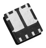


NVMFD5C470NWFT1G
Dual MOSFET, N Channel, 40 V, 36 A, 0.0117 ohm
- Manufacturer: ONSEMI
- Product type: Dual MOSFETs
- MSL: MSL 1 - Unlimited
- SVHC: Lead (25-Jun-2025)
- No. of Pins: 8Pins
- Channel Type: N Channel
- Product Range: -
- Qualification: -
- Transistor Case Style: DFN
- Operating Temperature Max: 175°C
- Power Dissipation N Channel: 28W
- Power Dissipation P Channel: -
- Drain Source Voltage Vds N Channel: 40V
- Drain Source Voltage Vds P Channel: -
- Continuous Drain Current Id N Channel: 36A
- Continuous Drain Current Id P Channel: -
- Drain Source On State Resistance N Channel: 0.0117ohm
- Drain Source On State Resistance P Channel: -
| Delivery and price | |
|---|---|
| Units per pack | 1500 |
| Price | 0.571 € |
| Current stock | 10+ |
| Lead time | 30 days |
**Share Feedback DATA SHEET** Your Opinion Matters **www.onsemi.com** ~~ee~~ ## MOSFET ~~SS~~ – Power, Dual **-** N Channel **==> picture [190 x 30] intentionally omitted <==** **----- Start of picture text -----**<br> V(BR)DSS RDS(ON) MAX ID MAX<br>40 V 11.7 m @ 10 V 36 A<br>ee e ee<br>**----- End of picture text -----**<br> ## 40 V, 11.7 m 36 A ## NVMFD5C470N ## **Features** - Small Footprint (5x6 mm) for Compact Design - Low R to Minimize Conduction Losses DS(on) - Low QG and Capacitance to Minimize Driver Losses - NVMFD5C470NWF − Wettable Flank Option for Enhanced Optical Inspection - AEC-Q101 Qualified and PPAP Capable - These Devices are Pb-Free and are RoHS Compliant **MAXIMUM RATINGS** (TJ = 25 ° C unless otherwise noted) |**Parameter**|**Parameter**|**Parameter**|**Symbol**|**Value**|**Unit**| |---|---|---|---|---|---| |Drain-to-Source Voltage|||VDSS|40|V| |Gate-to-Source Voltage<br>~~EE~~|||VGS<br>~~EE~~|±20<br>~~EE~~|V<br>~~EE~~| |Continuous Drain<br>Current R JC<br>(Notes 1, 2, 3)<br>~~EE~~<br>~~——s=8~~<br>~~Pe~~|Steady<br>State<br>~~EE~~<br>~~——s=8~~<br>|TC= 25°C<br>~~EE~~<br>~~——s=8~~|ID<br>~~EE~~<br>~~——s=8~~<br>~~—~~|36<br>~~EE~~<br>~~——s=8~~|A<br>~~EE~~<br>~~——s=8~~<br>~~—~~| |||TC= 100°C<br>~~——s=8~~<br>~~—~~||25<br>~~——s=8~~<br>~~—~~|| |Power Dissipation<br>R JC(Notes 1, 2)<br>~~——s=8~~<br>~~Pe~~||TC= 25°C<br>~~——s=8~~<br>~~—~~|PD<br>~~——s=8~~<br>~~—~~|28<br>~~——s=8~~<br>~~—~~|W<br>~~——s=8~~<br>~~—~~| |||TC= 100°C<br>~~——s=8~~<br>~~—~~||14<br>~~——s=8~~<br>~~—~~|| |Continuous Drain<br>Current R JA<br>(Notes 1, 2, 3)<br>~~Pe ~~<br>~~|~~<br>~~a ee~~|Steady<br>State<br> <br>~~|~~<br>~~ee ee~~<br>~~ee~~|TA= 25°C<br>~~—~~<br>~~|~~|ID<br>~~—~~<br>~~|~~<br>~~ee~~|11.7<br>~~—~~<br>~~|~~|A<br>~~—~~<br>~~|~~<br>~~ee~~| |||TA= 100°C<br> ~~—~~<br>~~|~~<br>~~ee~~||8.3<br>~~—~~<br>~~|~~<br>~~ee~~|| |Power Dissipation<br>R JA(Notes 1 & 2)<br>~~|~~<br>~~a ee~~||TA= 25°C<br>~~|~~<br>~~ee~~|PD<br>~~|~~<br>~~ee~~|3.1<br>~~|~~<br>~~ee~~|W<br>~~|~~<br>~~ee~~| |||TA= 100°C<br>~~|~~<br>~~ee~~<br>~~ee~~||1.5<br>~~|~~<br>~~ee~~|| |Pulsed Drain Current<br>~~a ee~~<br>~~ee~~|TA= 25°C, tp= 10 s<br>~~ee ee~~<br>~~ee~~<br>~~ee~~||IDM<br>~~ee~~<br>~~ee~~|108<br>~~ee~~<br>~~ee~~|A<br>~~ee~~<br>~~ee~~| |Operating Junction and Storage Temperature<br>~~ee~~<br>~~Po~~|||TJ, Tstg<br>~~Po~~<br>~~ee~~|−55 to<br>+ 175<br>~~Po~~<br>~~es~~|°C<br>~~Po~~| |Source Current (Body Diode)<br>~~ee~~|||IS<br>~~ee~~<br>~~ee~~|23<br>~~ee~~<br>~~es~~|A<br>~~ee~~| |Single Pulse Drain-to-Source Avalanche<br>Energy (TJ= 25°C, IL(pk)= 2 A)<br>~~Pe~~|||EAS<br>~~ee ~~<br>~~Pe~~<br>~~es~~|49<br> ~~es~~<br>~~Pe~~|mJ<br>~~Pe~~| |Lead Temperature for Soldering Purposes<br>(1/8″from case for 10 s)<br>~~es~~|||TL<br>~~es~~<br>~~es~~|260<br>~~es~~|°C<br>~~es~~| Stresses exceeding those listed in the Maximum Ratings table may damage the device. If any of these limits are exceeded, device functionality should not be assumed, damage may occur and reliability may be affected. **==> picture [179 x 209] intentionally omitted <==** **----- Start of picture text -----**<br> Dual N-Channel<br>D1 D2<br>G1 G2<br>S1 S2<br>MARKING<br>DIAGRAM<br>D1 D1<br>S1 D1<br>1<br>G1 XXXXXX D1<br>DFN8 5x6<br>S2 AYWZZ D2<br>(SO8FL)<br>G2 D2<br>CASE 506BT<br>D2 D2<br>**----- End of picture text -----**<br> XXXXXX = 5C470N (NVMFD5C470N) = or 470NWF (NVMFD5C470NWF) A = Assembly Location Y = Year W = Work Week ZZ = Lot Traceability ## **ORDERING INFORMATION** See detailed ordering, marking and shipping information on page 5 of this data sheet. ## **THERMAL RESISTANCE MAXIMUM RATINGS** ||~~Ge~~|~~ee~~|| |---|---|---|---| |**Parameter**<br>~~ee~~|**Symbol**<br>~~ee~~<br>~~Ge~~|**Value**<br>~~ee~~<br>~~ee~~|**Unit**<br>~~ee~~| |Junction-to-Case − Steady State|R JC<br>~~Ge~~|5.3<br>~~ee~~|°C/W| |Junction-to-Ambient − Steady State (Note 2)|R JA|49|| 1. The entire application environment impacts the thermal resistance values shown, they are not constants and are only valid for the particular conditions noted. 2. Surface-mounted on FR4 board using a 650 mm[2] , 2 oz. Cu pad. 3. Maximum current for pulses as long as 1 second is higher but is dependent on pulse duration and duty cycle. Publication Order Number: **NVMFD5C470N/D** **1** © Semiconductor Components Industries, LLC, 2017 **August, 2025 − Rev. 2** ## **NVMFD5C470N** **ELECTRICAL CHARACTERISTICS** (TJ = 25 ° C unless otherwise specified) |**ELECTRICAL CHARACTERISTICS**(TJ = 25J = 25= 25°C unless otherwise specified)|**ELECTRICAL CHARACTERISTICS**(TJ = 25J = 25= 25°C unless otherwise specified)|**ELECTRICAL CHARACTERISTICS**(TJ = 25J = 25= 25°C unless otherwise specified)|**ELECTRICAL CHARACTERISTICS**(TJ = 25J = 25= 25°C unless otherwise specified)|**ELECTRICAL CHARACTERISTICS**(TJ = 25J = 25= 25°C unless otherwise specified)| |---|---|---|---|---| |**Parameter**<br>**Symbol**<br>**Test Condition**<br>**Min**<br>**Typ**<br>**Max**<br>**Unit**<br>**OFF CHARACTERISTICS**<br>~~Po~~||||| |Drain-to-Source Breakdown Voltage|V(BR)DSS|VGS= 0 V, ID= 250 A|40|V| |Drain-to-Source Breakdown Voltage<br>Temperature Coefficient<br>~~a~~|V(BR)DSS/<br>TJ||24|mV/°C| |Zero Gate Voltage Drain Current<br>IDSS<br>VGS= 0 V,<br>VDS= 40 V<br>TJ= 25°C<br>10<br>A<br>TJ= 125°C<br>100<br>Gate-to-Source Leakage Current<br>IGSS<br>VDS= 0 V, VGS= 20 V<br>100<br>nA<br>**ON CHARACTERISTICS**(Note 4)<br>~~eo~~<br>~~ee~~<br>~~ee ee~~<br>~~pO~~||||| |Gate Threshold Voltage<br>Threshold Temperature Coefficient<br>~~po~~<br>~~a~~|VGS(TH)<br>VGS= VDS, ID= 250 A<br>2.5<br>3.5<br>V<br>VGS(TH)/TJ<br>−6.0<br>mV/°C<br>~~GO~~|||| |Drain-to-Source On Resistance<br>RDS(on)<br>VGS= 10 V<br>ID= 10 A<br>9.75<br>11.7<br>m<br>~~pO~~||||| |**CHARGES, CAPACITANCES & GATE RESISTANCE**||||| |Input Capacitance|CISS||420|| |Output Capacitance|COSS|VGS= 0 V, f = 1 MHz, VDS= 25 V|210|pF| |Reverse Transfer Capacitance|CRSS||11|| |Total Gate Charge|QG(TOT)||8.0|| |Threshold Gate Charge|QG(TH)||1.6|nC| |Gate-to-Source Charge|QGS|VGS= 10 V, VDS= 32 V; ID= 10 A|2.5|| |Gate-to-Drain Charge|QGD||1.5|| |Plateau Voltage|VGP||4.7|V| |**SWITCHING CHARACTERISTICS**(Note 5)||||| |Turn-On Delay Time<br>td(ON)<br>Rise Time<br>tr<br>Turn-Off Delay Time<br>td(OFF)<br>Fall Time<br>tf<br>**DRAIN-SOURCE DIODE CHARACTERISTICS**<br>~~ee ee~~<br>~~ee ee~~<br>~~ee ~~~~**ee**~~<br>~~ee~~||VGS= 10 V, VDS= 32 V,<br>ID= 10 A, RG= 1.0<br>,|8.0<br>14<br>16<br>4.5<br>~~| |~~<br> ~~-}~~<br>~~|~~<br>~~**|** |~~<br>~~|~~|ns| |Forward Diode Voltage<br>Reverse Recovery Time<br>Charge Time<br>Discharge Time<br>Reverse Recovery Charge<br>Product parametric performance is indicated in the Electrical Characteristics for the listed test conditions, unless otherwise noted. Product<br>~~a~~<br>~~ee ~~<br>~~ee ~~<br>~~ee ~~<br>~~ee~~|VSD<br>VGS= 0 V,<br>IS= 10 A<br>TJ= 25°C<br>0.9<br>1.2<br>V<br>TJ= 125°C<br>0.8<br>tRR<br>VGS= 0 V, dIS/dt = 100 A/ s,<br>IS= 10 A<br>20<br>ns<br>ta<br>9.0<br>tb<br>10<br>QRR<br>7.5<br>nC<br>Product parametric performance is indicated in the Electrical Characteristics for the listed test conditions, unless otherwise noted. Product<br>~~a~~<br>~~ee ee~~<br> ~~ee~~<br>~~|~~~~**|**~~<br> ~~ee~~<br>»<br>~~ft~~<br> ~~**ee**~~<br>~~| |~~<br>~~a a a~~|||| |performance may not be indicated by the Electrical Characteristics if operated under different conditions.||||| |4. Pulse Test: pulse width<br>300 s, duty cycle<br><<br>u|300 s, duty cycle<br>2%.<br><|||| 5. Switching characteristics are independent of operating junction temperatures. **www.onsemi.com** **Share Feedback** Your Opinion Matters **2** **NVMFD5C470N** ## **TYPICAL CHARACTERISTICS** **==> picture [490 x 618] intentionally omitted <==** **----- Start of picture text -----**<br> 200 40<br>VDS = 3 V<br>180 10 V 35<br>160 pf} fe ee ee ee ee,<br>9 V 30<br>140 ee<br>pee 25 PF |ffLK<br>120<br>8 V<br>100 4 4 20 ‘A<br>80 7 V 15<br>60 TJ = 25 ° C<br>Zea Ef<br>10<br>40 6 V<br>20 4 V 5 V 5 T J = 125 ° C TJ = −55 ° C<br>0 Zr 0 A Aa<br>0 0.5 1.0 1.5 2.0 2.5 3.0 3.0 3.5 4.0 4.5 5.0 5.5 6.0<br>VDS, DRAIN-TO-SOURCE VOLTAGE (V) VGS, GATE-TO-SOURCE VOLTAGE (V)<br>Figure 1. On-Region Characteristics Figure 2. Transfer Characteristics<br>40 15<br>35 TI D J = 25 = 10 A ° C 1413<br>ee Os<br>30<br>12 V GS = 10 V<br>25 ee 11<br>20 10<br>9<br>15<br>8<br>10<br>7<br>5 ee 6 ee<br>0 ee ee ee ee 5 a<br>4 5 6 7 8 9 10 0 10 20 30 40 50 60 70 80<br>VGS, GATE-TO-SOURCE VOLTAGE (V) ID, DRAIN CURRENT (A)<br>Figure 3. On-Resistance vs. Gate-to-Source Figure 4. On-Resistance vs. Drain Current and<br>Voltage Gate Voltage<br>1.9 10K<br>I D = 10 A | | [ | [| [ J SSS TJ = 150 ° C<br>1.7 VGS = 10 V<br>eee ——_—$—_———— ee<br>1.5 OnPf |OO|| || [|| || KfLA][| | 1K ———————eea eeseee ee ee TJ = 125 eee ° C<br>1.3<br>FERRE eS TJ = 85 ° C<br>1.1 OnSSeSA 100 eTSS<br>0.9<br>Cee<br>0.7 | | [| | | | fT [|| 10 a ee ee ee ee<br>−50 −25 0 25 50 75 100 125 150 175 5 10 15 20 25 30 35 40<br>TJ, JUNCTION TEMPERATURE ( ° C) VDS, DRAIN-TO-SOURCE VOLTAGE (V)<br>Figure 5. On-Resistance Variation with Figure 6. Drain-to-Source Leakage Current<br>Temperature vs. Voltage<br>, DRAIN CURRENT (A) , DRAIN CURRENT (A)<br>ID ID<br>) )<br>, DRAIN-TO-SOURCE RESISTANCE (m , DRAIN-TO-SOURCE RESISTANCE (m<br>DS(on) DS(on)<br>R R<br>, LEAKAGE (nA)<br>IDSS<br>, DRAIN-TO-SOURCE RESISTANCE (NORMALIZED)<br>DS(on)<br>R<br>**----- End of picture text -----**<br> **www.onsemi.com** **Share Feedback** Your Opinion Matters **3** **NVMFD5C470N** ## **TYPICAL CHARACTERISTICS** **==> picture [490 x 383] intentionally omitted <==** **----- Start of picture text -----**<br> 1K 10<br>SSS SS SS Ciss 9 P| | | | | | TY<br>a ee Coss 8<br>7<br>100<br>OH 6 Q SH gs HE Qgd SeHSH<br>5<br>4<br>10 Crss<br>| | fm | 3 TTA<br>TJ = 25 ° C ——————— 2 | Yi] | | | V DS = 32 V<br>VGS = 0 V ID = 10 A<br>f = 1 MHz Ee oo 1 LA | | | | | T J = 25 ° C<br>1 | ot | | tf 0 Yi [| | | | |<br>0 5 10 15 20 25 30 35 40 0 1 2 3 4 5 6 7 8 9<br>VDS, DRAIN-TO-SOURCE VOLTAGE (V) Qg, TOTAL GATE CHARGE (nC)<br>Figure 7. Capacitance Variation Figure 8. Gate-to-Source and Drain-to-Source<br>Voltage vs. Total Charge<br>RR es ee en ee 10 ee<br>i VGS = 0 V oe a<br>en td(off) SSS<br>aT e e eeeee oe<br>ey<br>tr<br>10 TT Ae ee<br>ce t d(on) SS cet Oe 1 yA /ae<br>t f<br>Bec —_——<br>VGS = 10 V<br>VDS = 32 V<br>TJ = 125 ° C TJ = 25 ° C TJ = −55 ° C<br>1 0.1 ASAE<br>coin.) } =F<br>1 10 0.4 0.5 0.6 0.7 0.8 0.9 1.0<br>RG, GATE RESISTANCE ( Q ) VSD, SOURCE-TO-DRAIN VOLTAGE (V)<br>C, CAPACITANCE (pF)<br>, GATE-TO-SOURCE VOLTAGE (V)<br>GS<br>V<br>t, TIME (ns)<br>, SOURCE CURRENT (A)<br>IS<br>**----- End of picture text -----**<br> **Figure 9. Resistive Switching Time Variation vs. Gate Resistance** **Figure 10. Diode Forward Voltage vs. Current** **==> picture [489 x 172] intentionally omitted <==** **----- Start of picture text -----**<br> 1000 100<br>TC = 25 ° C<br>VGS ≤ 10 V<br>100 Single Pulse Code o T Ceti TJ(initial) = 25 ° C cot<br>10<br>10<br>10 s<br>1 TJ(initial) = 100 ° C<br>FEE REE pf LE NT<br>1<br>Thermal LimitRDS(on) Limit WY 10.5 msms at a<br>10 ms<br>Package Limit<br>0.1 — — e:i: eaCoil 0.1 aeell<br>0.1 1 10 100 1000 1.0E−05 1.0E−04 1.0E−03 1.0E−02<br>VDS, DRAIN-TO-SOURCE VOLTAGE (V) TIME IN AVALANCHE (s)<br> (A)<br>IPEAK<br>, DRAIN CURRENT (A)<br>ID<br>**----- End of picture text -----**<br> **Figure 11. Maximum Rated Forward Biased Safe Operating Area** **Figure 12. Maximum Drain Current vs. Time in Avalanche** **www.onsemi.com** **Share Feedback** Your Opinion Matters **4** **NVMFD5C470N** ## **TYPICAL CHARACTERISTICS** **==> picture [489 x 173] intentionally omitted <==** **----- Start of picture text -----**<br> 100 —S_—_ee =... a— __--..-A A ==...EO=... SG==eeSG==...ESee===.EE OG =GG SEOOee SS SSeee<br>BE 50% Duty Cycle SGSS OS<br>10 eisl=ee 20% 10%5% OOOOSSaee [SS] Lf————=== ==EE ———=.eT ee eTeeeae_ = ===eeEeerit==AAUeeeEE eee===i|Eee| ETI eeEee|llMAlllTT<br>2% PTT [eer TT TTT TT TTT TTT TPTPT<br>1 —— [ee] ca [A] [0] 00|<br>Sr a ee ee eee<br>1% a RO A OO SO OS NOE OO SG EGE EO OG ES GSS EE OO GS OO<br>SSeetSSS et<br>0.1 Single Pulse<br>a0pee ere eee EE0eee eee eeea eee0eee eee0 eee eee0eee eeeOOeee eee ee eee<br>0.01<br>0.000001 0.00001 0.0001 0.001 0.01 0.1 1 10 100 1000<br>PULSE TIME (sec)<br>C/W)<br>°<br>R(t) (<br>**----- End of picture text -----**<br> **Figure 13. Thermal Response** ## **DEVICE ORDERING INFORMATION** |**Device**|**Marking**|**Package**|**Shipping**†| |---|---|---|---| |NVMFD5C470NT1G|5C470N|DFN8<br>(Pb-Free)|1500 / Tape & Reel| |NVMFD5C470NWFT1G|470NWF|DFN8<br>(Pb-Free, Wettable Flanks)|1500 / Tape & Reel| †For information on tape and reel specifications, including part orientation and tape sizes, please refer to our Tape and Reel Packaging Specifications Brochure, BRD8011/D. **www.onsemi.com** **Share Feedback** Your Opinion Matters **5** **NVMFD5C470N** ## **REVISION HISTORY** |**Revision**<br>**Description of Changes**<br>**Date**<br>2<br>Document rebranded to**onsemi**format.<br>8/27/2025<br>This document has undergone updates prior to the inclusion of this revision history table. The changes tracked here only reflect updates made<br>~~—~~| |---| |on the noted approval dates.| > **www.onsemi.com Share Feedback** ~~SS?~~ **6** Your Opinion Matters MECHANICAL CASE OUTLINE **PACKAGE DIMENSIONS** **==> picture [51 x 34] intentionally omitted <==** **DFN8 5x6, 1.27P Dual Flag (SO8FL−Dual)** CASE 506BT ISSUE F DATE 23 NOV 2021 **==> picture [477 x 500] intentionally omitted <==** **----- Start of picture text -----**<br> 1 DATE 23 NOV 2021<br>SCALE 2:1 2X NOTES:<br>0.20 C 1. DIMENSIONING AND TOLERANCING PER ASME Y14.5M, 1994.<br>2. CONTROLLING DIMENSION: MILLIMETERS.<br>D A 3. DIMENSION b APPLIES TO PLATED TERMINAL AND IS MEASURED<br>BETWEEN 0.15 AND 0.30 MM FROM THE TERMINAL TIP.<br>8 7 D16 5 B 2X 0.20 C 4.5. PROFILE TOLERANCE APPLIES TO THE EXPOSED PAD AS WELLAS THE TERMINALS.DIMENSIONS D1 AND E1 DO NOT INCLUDE MOLD FLASH,PROTRUSIONS, OR GATE BURRS.<br>6. SEATING PLANE IS DEFINED BY THE TERMINALS. A1 IS DEFINED<br>AS THE DISTANCE FROM THE SEATING PLANE TO THE LOWEST<br>POINT ON THE PACKAGE BODY.<br>7. A VISUAL INDICATOR FOR PIN 1 MUST BE LOCATED IN THIS AREA.<br>PIN ONE E1 E MILLIMETERS<br>IDENTIFIER<br>ÉÉ DIM MIN NOM MAX<br>NOTE 7 A 0.90 −−− 1.10<br>ÉÉ 4Xh A1b 0.33−−− 0.42−−− 0.050.51<br>1 2 3 4 b1 0.33 0.42 0.51<br>ÉÉ c 0.20 −−− 0.33<br>TOP VIEW c A1 D 5.15 BSC<br>D1 4.70 4.90 5.10<br>0.10 C D2 3.90 4.10 4.30<br>A D3 1.50 1.70 1.90<br>DETAIL B E 6.15 BSC<br>0.10 C ALTERNATE E1 5.70 5.90 6.10<br>NOTE 4 SIDE VIEW C [SEATING] PLANE DETAIL A CONSTRUCTION E2e 3.90 1.27 BSC4.15 4.40<br>DETAIL A NOTE 6 G 0.45 0.55 0.65<br>h −−− −−− 12 �<br>D2 K 0.51 −−− −−−<br>D3 K1 0.56 −−− −−−<br>L 0.48 0.61 0.71<br>e 4X L M 3.25 3.50 3.75<br>1 4 K N 1.80 2.00 2.20<br>DETAIL B SOLDERING FOOTPRINT*<br>4.56<br>M N 4Xb1 E2 0.758X 2.082X 0.562X<br>8 5<br>4X G 8X b<br>K1 0.10 C A B 4X<br>4.84 1.40 6.59<br>BOTTOM VIEW 0.05 C NOTE 3 2.30<br>3.70<br>GENERIC<br>MARKING DIAGRAM*<br>0.70<br>1<br>XXXXXX<br>AYWZZ 4X 1.00 1.27<br>PITCH<br>XXXXXX = Specific Device Code 5.55<br>A = Assembly Location DIMENSION: MILLIMETERS<br>Y = Year<br>*For additional information on our Pb−Free strategy and soldering<br>W = Work Week details, please download the onsemi Soldering and Mounting<br>ZZ = Lot Traceability Techniques Reference Manual, SOLDERRM/D.<br>**----- End of picture text -----**<br> 7. A VISUAL INDICATOR FOR PIN 1 MUST BE LOCATED IN THIS AREA. **==> picture [207 x 186] intentionally omitted <==** **----- Start of picture text -----**<br> 4.56<br>2X 2X<br>8X 2.082X 0.562X<br>0.758X<br>4X<br>4.84 1.40 6.59<br>2.30<br>3.70<br>0.70<br>4X 1.00 1.27<br>PITCH<br>5.55<br>DIMENSION: MILLIMETERS<br>**----- End of picture text -----**<br> - *For additional information on our Pb−Free strategy and soldering details, please download the **onsemi** Soldering and Mounting Techniques Reference Manual, SOLDERRM/D. - *This information is generic. Please refer to device data sheet for actual part marking. Pb−Free indicator, “G” or microdot “ � ”, may or may not be present. Some products may not follow the Generic Marking. Electronic versions are uncontrolled except when accessed directly from the Document Repository. Printed versions are uncontrolled except when stamped “CONTROLLED COPY” in red. ## **DOCUMENT NUMBER: 98AON50417E** **DESCRIPTION: DFN8 5X6, 1.27P DUAL FLAG (SO8FL−DUAL)** **PAGE 1 OF 1** **onsemi** and are trademarks of Semiconductor Components Industries, LLC dba **onsemi** or its subsidiaries in the United States and/or other countries. **onsemi** reserves the right to make changes without further notice to any products herein. **onsemi** makes no warranty, representation or guarantee regarding the suitability of its products for any particular purpose, nor does **onsemi** assume any liability arising out of the application or use of any product or circuit, and specifically disclaims any and all liability, including without limitation special, consequential or incidental damages. **onsemi** does not convey any license under its patent rights nor the rights of others. www.onsemi.com © Semiconductor Components Industries, LLC, 2011 **onsemi** , , and other names, marks, and brands are registered and/or common law trademarks of Semiconductor Components Industries, LLC dba “ **onsemi** ” or its affiliates and/or subsidiaries in the United States and/or other countries. **onsemi** owns the rights to a number of patents, trademarks, copyrights, trade secrets, and other intellectual property. A listing of **onsemi** ’s product/patent coverage may be accessed at www.onsemi.com/site/pdf/Patent−Marking.pdf. **onsemi** reserves the right to make changes at any time to any products or information herein, without notice. The information herein is provided “as−is” and **onsemi** makes no warranty, representation or guarantee regarding the accuracy of the information, product features, availability, functionality, or suitability of its products for any particular purpose, nor does **onsemi** assume any liability arising out of the application or use of any product or circuit, and specifically disclaims any and all liability, including without limitation special, consequential or incidental damages. Buyer is responsible for its products and applications using **onsemi** products, including compliance with all laws, regulations and safety requirements or standards, regardless of any support or applications information provided by **onsemi** . “Typical” parameters which may be provided in **onsemi** data sheets and/or specifications can and do vary in different applications and actual performance may vary over time. All operating parameters, including “Typicals” must be validated for each customer application by customer’s technical experts. **onsemi** does not convey any license under any of its intellectual property rights nor the rights of others. **onsemi** products are not designed, intended, or authorized for use as a critical component in life support systems or any FDA Class 3 medical devices or medical devices with a same or similar classification in a foreign jurisdiction or any devices intended for implantation in the human body. Should Buyer purchase or use **onsemi** products for any such unintended or unauthorized application, Buyer shall indemnify and hold **onsemi** and its officers, employees, subsidiaries, affiliates, and distributors harmless against all claims, costs, damages, and expenses, and reasonable attorney fees arising out of, directly or indirectly, any claim of personal injury or death associated with such unintended or unauthorized use, even if such claim alleges that **onsemi** was negligent regarding the design or manufacture of the part. **onsemi** is an Equal Opportunity/Affirmative Action Employer. This literature is subject to all applicable copyright laws and is not for resale in any manner. ## **ADDITIONAL INFORMATION** **TECHNICAL PUBLICATIONS** : **ONLINE SUPPORT** : www.onsemi.com/support **Technical Library:** www.onsemi.com/design/resources/technical−documentation **For additional information, please contact your local Sales Representative at onsemi Website:** www.onsemi.com www.onsemi.com/support/sales **==> picture [232 x 43] intentionally omitted <==**
Updated at June 9, 2026
onsemi is a premier global supplier of intelligent power and sensing technologies, driving disruptive innovations across the automotive, industrial, and cloud infrastructure markets. Recognized for their commitment to sustainability and reliable supply chains, the company accelerates advancements in vehicle electrification, industrial automation, and 5G networks by solving the industry's most complex design challenges. At the core of their portfolio is an industry-leading selection of discrete semiconductors. This extensive range features thousands of high-performance bipolar transistors, single and dual MOSFETs, and a comprehensive array of diodes, including Zener, Schottky, and fast-recovery rectifiers. Engineered for superior thermal performance and energy efficiency, these foundational components are critical for demanding power conversion, switching, and signal conditioning applications. Beyond essential discretes, onsemi provides a robust suite of advanced power management and circuit protection solutions. Their lineup includes intelligent power modules, single IGBTs, and transient voltage suppression (TVS) diodes designed to safeguard sensitive circuitry. Complimented by integrated passive filters, AC/DC LED driver ICs, and specialized sub-2.4GHz RF transceivers, onsemi equips engineers with the scalable, high-quality technologies needed to build a cleaner, smarter, and more connected world.
About Novapart
Novapart is a B2B electronic component broker specialising in stock shortages and cost reduction. We source hard-to-find parts and identify compliant alternatives across a catalogue of 410,000+ components from 500+ manufacturers.
Learn more →Stock Shortage Specialist
When a component is unavailable, discontinued or has an unacceptable lead time, we tap into our network of vetted European and Asian distributors to source what you need — without compromising on quality or traceability.
Request a quote →Compliant Alternatives
We identify pin-to-pin, electrically equivalent substitutes that meet the same certifications (RoHS, AEC-Q100, REACH) as your original specification — validated against datasheets, not just part numbers. Often at a lower cost.
BOM Analysis service →