


NVD3055L170T4G-VF01
Power MOSFET, N Channel, 60 V, 9 A, 0.153 ohm, TO-252 (DPAK), Surface Mount
- Manufacturer: ONSEMI
- Product type: Single MOSFETs
- No. of Pins: 3Pins
- Channel Type: N Channel
- Qualification: AEC-Q101
- Power Dissipation: 28.5W
- Transistor Mounting: Surface Mount
- Transistor Polarity: N Channel
- Power Dissipation Pd: 28.5W
- Rds(on) Test Voltage: 5V
- On Resistance Rds(on): 0.153ohm
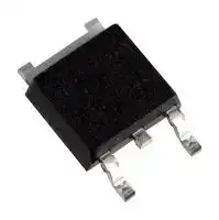
- Transistor Case Style: TO-252 (DPAK)
- Drain Source Voltage Vds: 60V
- Operating Temperature Max: 175°C
- Continuous Drain Current Id: 9A
- Drain Source On State Resistance: 0.153ohm
- Automotive Qualification Standard: AEC-Q101
- Gate Source Threshold Voltage Max: 1.7V
| Delivery and price | |
|---|---|
| Units per pack | 500 |
| Price | 0.465 € |
| Current stock | 10+ |
| Lead time | 7 days |
## NTD3055L170, NVD3055L170

## MOSFET – Power, N-Channel, Logic Level, DPAK/IPAK 9.0 A, 60 V

Designed for low voltage, high speed switching applications in power supplies, converters and power motor controls and bridge circuits.

## **Features**

- NVD Prefix for Automotive and Other Applications Requiring Unique Site and Control Change Requirements; AEC−Q101 Qualified and PPAP Capable

- These are Pb−Free Devices

## **Typical Applications**

- Power Supplies

- Converters

- Power Motor Controls

- Bridge Circuits

**MAXIMUM RATINGS** (TJ = 25 ° C unless otherwise noted)

|**Rating**<br>~~BS~~|**Symbol**<br>~~BS~~|**Value**<br>~~BS~~|**Unit**<br>~~BS~~|
|---|---|---|---|
|Drain−to−Source Voltage<br>~~BS~~|VDSS<br>~~BS~~|60<br>~~BS~~|Vdc<br>~~BS~~|
|Drain−to−Gate Voltage (RGS= 10 M )<br>~~BS~~|VDGR<br>~~BS~~|60<br>~~BS~~|Vdc<br>~~BS~~|
|Gate−to−Source Voltage<br>− Continuous<br>− Non−repetitive (tp<br>10 ms)<br>~~poe~~|VGS<br>VGS<br>~~poe~~|±15<br>±20<br>~~poe~~|Vdc<br>~~poe~~|
|Drain Current<br>− Continuous @ TA= 25°C<br>− Continuous @ TA= 100°C<br>− Single Pulse (tp<br>10 s)<br>~~a~~|ID<br>ID<br>IDM<br>~~a~~|9.0<br>3.0<br>27<br>~~a~~|Adc<br>Apk<br>~~a~~|
|Total Power Dissipation @ TA= 25°C<br>Derate above 25°C<br>Total Power Dissipation @ TA= 25°C (Note 1)<br>Total Power Dissipation @ TA= 25°C (Note 2)<br>~~a~~<br>~~a~~<br>~~ee~~|PD<br>~~a~~<br>~~a~~<br>~~ee~~|28.5<br>0.19<br>2.1<br>1.5<br>~~a~~<br>~~a~~<br>~~ee~~|W<br>W/°C<br>W<br>W<br>~~a~~<br>~~a~~<br>~~ee~~|
|Operating and Storage Temperature Range<br>~~ee~~|TJ, Tstg<br>~~ee~~|−55 to<br>175<br>~~ee~~|°C<br>~~ee~~|
|Single Pulse Drain−to−Source Avalanche<br>Energy − Starting TJ= 25°C<br>(VDD= 25 Vdc, VGS= 5.0 Vdc,<br>L = 1.0 mH, IL(pk) = 7.75 A, VDS= 60 Vdc)<br>~~ee ~~<br>~~es~~|EAS<br> ~~ee~~<br>~~es~~|30<br>~~ee~~<br>~~es~~|mJ<br>~~ee~~<br>~~es~~|
|Thermal Resistance<br>− Junction−to−Case<br>− Junction−to−Ambient (Note 1)<br>− Junction−to−Ambient (Note 2)<br>~~po~~|R JC<br>R JA<br>R JA<br>~~po~~<br>~~ee~~|5.2<br>71.4<br>100<br>~~po~~<br>~~ee~~|°C/W<br>~~po~~|
|Maximum Lead Temperature for Soldering<br>Purposes, 1/8″from case for 10 seconds<br>~~ee~~|TL<br>~~ee~~<br>~~ee~~|260<br>~~ee~~<br>~~ee~~|°C<br>~~ee~~|


## **www.onsemi.com**

## **9.0 AMPERES, 60 VOLTS R = 170 m DS(on)**

**==> picture [159 x 201] intentionally omitted <==**

**----- Start of picture text -----**<br>
D<br>N−Channel<br>G<br>S<br>4<br>4<br>1<br>1 » [2] *<br>3 2 3<br>DPAK IPAK<br>CASE 369C CASE 369D<br>(Surface Mounted) (Straight Lead)<br>STYLE 2 STYLE 2<br>**----- End of picture text -----**<br>


**==> picture [141 x 190] intentionally omitted <==**

**----- Start of picture text -----**<br>
MARKING DIAGRAMS<br>& PIN ASSIGNMENTS<br>1 − Gate<br>AYWW 4<br>2 − Drain 31 Drain<br>70LG<br>3 − Source<br>e e e<br>1 − Gate<br>AYWW<br>4<br>2 − Drain 31<br>Drain<br>70LG<br>3 − Source<br>A = Assembly Location*<br>Y =  Year<br>WW = Work Week<br>3170L = Device Code<br>G = Pb−Free Package<br>**----- End of picture text -----**<br>


* The Assembly Location code (A) is front side optional. In cases where the Assembly Location is stamped in the package, the front side assembly code may be blank.

## **ORDERING INFORMATION**

See detailed ordering and shipping information in the package dimensions section on page 8 of this data sheet.

Publication Order Number: **NTD3055L170/D**

**1**

© Semiconductor Components Industries, LLC, 2014 **May, 2019 − Rev. 7**

**NTD3055L170, NVD3055L170**

1. When surface mounted to an FR4 board using 0.5 sq in pad size. 2. When surface mounted to an FR4 board using minimum recommended pad size.

**www.onsemi.com**

**2**

**NTD3055L170, NVD3055L170**

## **ELECTRICAL CHARACTERISTICS** (TJ = 25 ° C unless otherwise noted)

|**ELECTRICAL CHARACTERISTICS **(TJ= 25°C unless otherwise noted)|**ELECTRICAL CHARACTERISTICS **(TJ= 25°C unless otherwise noted)||||||
|---|---|---|---|---|---|---|
|**Characteristic**||**Symbol**|**Min**|**Typ**|**Max**|**Unit**|
|**OFF CHARACTERISTICS**|||||||
|Drain−to−Source Breakdown Voltage (Note 3)<br>(VGS= 0 Vdc, ID= 250�Adc)<br>Temperature Coefficient (Positive)||V(BR)DSS|60<br>−|−<br>53.6|−<br>−|Vdc<br>mV/°C|
|Zero Gate Voltage Drain Current<br>(VDS= 60 Vdc, VGS= 0 Vdc)<br>(VDS= 60 Vdc, VGS= 0 Vdc, TJ= 150°C)||IDSS|−<br>−|−<br>−|1.0<br>10|�Adc|
|Gate−BodyLeakage Current (VGS=±15 Vdc, VDS= 0 Vdc)||IGSS|−|−|±100|nAdc|
|**ON CHARACTERISTICS**(Note 3)|||||||
|Gate Threshold Voltage (Note 3)<br>(VDS= VGS, ID= 250�Adc)<br>Threshold Temperature Coefficient (Negative)||VGS(th)|1.0<br>−|1.7<br>4.2|2.0<br>−|Vdc<br>mV/°C|
|Static Drain−to−Source On−Resistance (Note 3)<br>(VGS= 5.0 Vdc, ID= 4.5 Adc)||RDS(on)|−|153|170|m�|
|Static Drain−to−Source On−Voltage (Note 3)<br>(VGS= 5.0 Vdc, ID= 9.0 Adc)<br>(VGS= 5.0 Vdc, ID= 4.5 Adc, TJ= 150°C)||VDS(on)|−<br>−|1.8<br>1.3|2.1<br>−|Vdc|
|Forward Transconductance (Note 3) (VDS= 8.0 Vdc, ID= 6.0 Adc)||gFS|−|7.3|−|mhos|
|**DYNAMIC CHARACTERISTICS**|||||||
|Input Capacitance|(VDS= 25 Vdc, VGS= 0 Vdc,<br>f = 1.0 MHz)|Ciss|−|195|275|pF|
|Output Capacitance||Coss|−|70|100||
|Transfer Capacitance||Crss|−|29|42||
|**SWITCHING CHARACTERISTICS**(Note 4)|||||||
|Turn−On Delay Time|(VDD= 30 Vdc, ID= 9.0 Adc,<br>VGS= 5.0 Vdc,<br>RG= 9.1�) (Note 3)|td(on)|−|9.7|20|ns|
|Rise Time||tr|−|69|150||
|Turn−Off Delay Time||td(off)|−|10|20||
|Fall Time||tf|−|38|80||
|Gate Charge|(VDS= 48 Vdc, ID= 9.0 Adc,<br>VGS= 5.0 Vdc) (Note 3)|QT|−|4.7|10|nC|
|||Q1|−|1.4|−||
|||Q2|−|2.9|−||
|**SOURCE−DRAIN DIODE CHARACTERISTICS**|||||||
|Forward On−Voltage|(IS= 9.0 Adc, VGS= 0 Vdc) (Note 3)<br>(IS= 9.0 Adc, VGS= 0 Vdc, TJ= 150°C)|VSD|−<br>−|0.98<br>0.85|1.25<br>−|Vdc|
|Reverse Recovery Time|(IS= 9.0 Adc, VGS= 0 Vdc,<br>dIS/dt = 100 A/�s) (Note 3)|trr|−|29.8|−|ns|
|||ta|−|17.6|−||
|||tb|−|12.2|−||
|Reverse RecoveryStored Charge||QRR|−|0.031|−|�C|


Product parametric performance is indicated in the Electrical Characteristics for the listed test conditions, unless otherwise noted. Product performance may not be indicated by the Electrical Characteristics if operated under different conditions.

3. Pulse Test: Pulse Width ≤ 300 � s, Duty Cycle ≤ 2%.

4. Switching characteristics are independent of operating junction temperatures.

**www.onsemi.com**

**3**

**NTD3055L170, NVD3055L170**

**==> picture [238 x 174] intentionally omitted <==**

**----- Start of picture text -----**<br>
20<br>VGS = 10 V<br>16<br>8 V 5 V<br>6 V<br>12<br>4 V<br>8<br>3.5 V<br>4<br>3 V<br>0<br>0 1 2 3 4 5 6 7 8<br>VDS, DRAIN−TO−SOURCE VOLTAGE (VOLTS)<br>, DRAIN CURRENT (AMPS)<br>ID<br>**----- End of picture text -----**<br>


**Figure 1. On−Region Characteristics**

**==> picture [231 x 174] intentionally omitted <==**

**----- Start of picture text -----**<br>
16<br>VDS ≥  10 V<br>12<br>8<br>4<br>TJ = 25 ° C<br>TJ = 100 ° C TJ = −55 ° C<br>0<br>1 1.5 2 2.5 3 3.5 4 4.5 5 5.5 6<br>VGS, GATE−TO−SOURCE VOLTAGE (VOLTS)<br>, DRAIN CURRENT (AMPS)<br>ID<br>**----- End of picture text -----**<br>


**Figure 2. Transfer Characteristics**

**==> picture [489 x 408] intentionally omitted <==**

**----- Start of picture text -----**<br>
0.35 0.35<br>VGS = 10 V<br>VGS = 15 V<br>0.3 0.3<br>0.25 TJ = 100 ° C 0.25<br>TJ = 100 ° C<br>0.2 TJ = 25 ° C 0.2<br>0.15 0.15 TJ = 25 ° C<br>TJ = −55 ° C<br>0.1 0.1<br>0.05 0.05 TJ = −55 ° C<br>0 0<br>4 6 8 10 12 14 16 18 4 8 12 16 20 24<br>ID, DRAIN CURRENT (AMPS) ID, DRAIN CURRENT (AMPS)<br>Figure 3. On−Resistance versus Figure 4. On−Resistance versus Drain Current<br>Gate−to−Source Voltage and Gate Voltage<br>2.2 1000<br>ID = 4.5 A VGS = 0 V<br>2 V GS = 5 V<br>TJ = 150 ° C<br>1.8<br>100<br>1.6<br>1.4 TJ = 125 ° C<br>1.2<br>10<br>1<br>TJ = 100 ° C<br>0.8<br>0.6 1<br>−50 −25 0 25 50 75 100 125 150 175 0 10 20 30 40 50 60<br>TJ, JUNCTION TEMPERATURE ( ° C) VDS, DRAIN−TO−SOURCE VOLTAGE (VOLTS)<br>) � ) �<br>, DRAIN−TO−SOURCE RESISTANCE ( , DRAIN−TO−SOURCE RESISTANCE (<br>DS(on) DS(on)<br>R R<br>, LEAKAGE (nA)<br>(NORMALIZED) IDSS<br>, DRAIN−TO−SOURCE RESISTANCE<br>DS(on)<br>R<br>**----- End of picture text -----**<br>


**Figure 5. On−Resistance Variation with Temperature**

**Figure 6. Drain−to−Source Leakage Current versus Voltage**

**www.onsemi.com**

**4**

**NTD3055L170, NVD3055L170**

## **POWER MOSFET SWITCHING**

Switching behavior is most easily modeled and predicted by recognizing that the power MOSFET is charge controlled. The lengths of various switching intervals (�t) are determined by how fast the FET input capacitance can be charged by current from the generator.

The published capacitance data is difficult to use for calculating rise and fall because drain−gate capacitance varies greatly with applied voltage. Accordingly, gate charge data is used.  In most cases, a satisfactory estimate of average input current (IG(AV)) can be made from a rudimentary analysis of the drive circuit so that

t = Q/IG(AV)

During the rise and fall time interval when switching a resistive load, VGS remains virtually constant at a level known as the plateau voltage, VSGP.  Therefore, rise and fall times may be approximated by the following:

tr = Q2 x RG/(VGG − VGSP)

tf = Q2 x RG/VGSP

## where

VGG = the gate drive voltage, which varies from zero to VGG RG = the gate drive resistance

and Q2 and VGSP are read from the gate charge curve.

During the turn−on and turn−off delay times, gate current is not constant.  The simplest calculation uses appropriate values from the capacitance curves in a standard equation for voltage change in an RC network.  The equations are:

The capacitance (Ciss) is read from the capacitance curve at a voltage corresponding to the off−state condition when calculating td(on) and is read at a voltage corresponding to the on−state when calculating td(off).

At high switching speeds, parasitic circuit elements complicate the analysis. The inductance of the MOSFET source lead, inside the package and in the circuit wiring which is common to both the drain and gate current paths, produces a voltage at the source which reduces the gate drive current. The voltage is determined by Ldi/dt, but since di/dt is a function of drain current, the mathematical solution is complex. The MOSFET output capacitance also complicates the mathematics. And finally, MOSFETs have finite internal gate resistance which effectively adds to the resistance of the driving source, but the internal resistance is difficult to measure and, consequently, is not specified.

The resistive switching time variation versus gate resistance (Figure 9) shows how typical switching performance is affected by the parasitic circuit elements.  If the parasitics were not present, the slope of the curves would maintain a value of unity regardless of the switching speed. The circuit used to obtain the data is constructed to minimize common inductance in the drain and gate circuit loops and is believed readily achievable with board mounted components.  Most power electronic loads are inductive; the data in the figure is taken with a resistive load, which approximates an optimally snubbed inductive load.  Power MOSFETs may be safely operated into an inductive load; however, snubbing reduces switching losses.

td(on) = RG Ciss In [VGG/(VGG − VGSP)]

td(off) = RG Ciss In (VGG/VGSP)

**==> picture [242 x 171] intentionally omitted <==**

**----- Start of picture text -----**<br>
700<br>VDS = 0 V VGS = 0 V TJ = 25 ° C<br>600<br>500 Ciss<br>400<br>300 Crss<br>Ciss<br>200<br>100 Coss<br>0 Crss<br>10 5 0 5 10 15 20 25<br>VGS VDS<br>C, CAPACITANCE (pF)<br>**----- End of picture text -----**<br>


**==> picture [244 x 9] intentionally omitted <==**

**----- Start of picture text -----**<br>
GATE−TO−SOURCE OR DRAIN−TO−SOURCE VOLTAGE (VOLTS)<br>**----- End of picture text -----**<br>


**Figure 7. Capacitance Variation**

**www.onsemi.com**

**5**

**NTD3055L170, NVD3055L170**

**==> picture [490 x 401] intentionally omitted <==**

**----- Start of picture text -----**<br>
6 1000<br>Q T<br>5 Q1 Q2<br>4 100<br>tr<br>3 tf<br>VGS<br>td(off)<br>2 10<br>td(on) VDS = 30 V<br>1 ID = 9 A ID = 9 A<br>TJ = 25 ° C VGS = 5 V<br>0 1<br>0 1 2 3 4 5 1 10 100<br>QG, TOTAL GATE CHARGE (nC) RG, GATE RESISTANCE (OHMS)<br>Figure 8. Gate−To−Source and Drain−To−Source Figure 9. Resistive Switching Time<br>Voltage versus Total Charge Variation versus Gate Resistance<br>DRAIN−TO−SOURCE DIODE CHARACTERISTICS<br>10<br>VGS = 0 V<br>TJ = 25 ° C<br>8<br>6<br>4<br>2<br>0<br>0.6 0.64 0.68 0.72 0.76 0.8 0.84 0.88 0.92 0.96<br>VSD, SOURCE−TO−DRAIN VOLTAGE (VOLTS)<br>t, TIME (ns)<br>VGS, GATE−TO−SOURCE VOLTAGE (VOLTS)<br>IS, SOURCE CURRENT (AMPS)<br>**----- End of picture text -----**<br>


**Figure 10. Diode Forward Voltage versus Current**

## **SAFE OPERATING AREA**

The Forward Biased Safe Operating Area curves define the maximum simultaneous drain−to−source voltage and drain current that a transistor can handle safely when it is forward biased. Curves are based upon maximum peak junction temperature and a case temperature (TC) of 25°C. Peak repetitive pulsed power limits are determined by using the thermal response data in conjunction with the procedures discussed in AN569, “Transient Thermal Resistance − General Data and Its Use.”

Switching between the off−state and the on−state may traverse any load line provided neither rated peak current (IDM) nor rated voltage (VDSS) is exceeded and the transition time (tr,tf) do not exceed 10 �s. In addition the total power averaged over a complete switching cycle must not exceed (TJ(MAX) − TC)/(R�JC).

A Power MOSFET designated E−FET can be safely used in switching circuits with unclamped inductive loads. For

reliable operation, the stored energy from circuit inductance dissipated in the transistor while in avalanche must be less than the rated limit and adjusted for operating conditions differing from those specified. Although industry practice is to rate in terms of energy, avalanche energy capability is not a constant. The energy rating decreases non−linearly with an increase of peak current in avalanche and peak junction temperature.

Although many E−FETs can withstand the stress of drain−to−source avalanche at currents up to rated pulsed current (IDM), the energy rating is specified at rated continuous current (ID), in accordance with industry custom. The energy rating must be derated for temperature as shown in the accompanying graph (Figure 12). Maximum energy at currents below rated continuous ID can safely be assumed to equal the values indicated.

**www.onsemi.com**

**6**

**NTD3055L170, NVD3055L170**

## **SAFE OPERATING AREA**

**==> picture [486 x 394] intentionally omitted <==**

**----- Start of picture text -----**<br>
100 32<br>V GS  = 15 V  ID = 7.75 A<br>SINGLE PULSE<br>TC = 25C = 25 = 25 ° C<br>24<br>10<br>10  � s<br>16<br>100  � s<br>1 ms<br>1<br>RDS(on) LIMITDS(on) LIMIT LIMIT 8<br>THERMAL LIMIT<br>10 ms<br>PACKAGE LIMIT<br>dc<br>0.1 0<br>0.1 1 10 100 25 50 75 100 125 150 175<br>VDS, DRAIN−TO−SOURCE VOLTAGE (VOLTS)DS, DRAIN−TO−SOURCE VOLTAGE (VOLTS), DRAIN−TO−SOURCE VOLTAGE (VOLTS) TJ, STARTING JUNCTION TEMPERATURE ( ° C)<br>Figure 11. Maximum Rated Forward Biased Figure 12. Maximum Avalanche Energy versus<br>Safe Operating Area Starting Junction Temperature<br>10<br>D = 0.5<br>0.2<br>1 0.1 P(pk)<br>0.05 R � JC(t) = r(t) R � JC<br>D CURVES APPLY FOR POWER<br>0.01 PULSE TRAIN SHOWN<br>t1 READ TIME AT t1<br>t2 TJ(pk) − TC = P(pk) R � JC(t)<br>SINGLE PULSE DUTY CYCLE, D = t1/t2<br>001<br>0.00001 0.0001 0.001 0.01 0.1 1 10<br>t, TIME ( � s)<br>AVALANCHE ENERGY (mJ)<br>EAS, SINGLE PULSE DRAIN−TO−SOURCE<br>(NORMALIZED)<br>r(t), EFFECTIVE TRANSIENT THERMAL RESISTANCE<br>**----- End of picture text -----**<br>


**==> picture [237 x 171] intentionally omitted <==**

**----- Start of picture text -----**<br>
100<br>V GS  = 15 V<br>SINGLE PULSE<br>TC = 25C = 25 = 25 ° C<br>10<br>10  � s<br>100  � s<br>1 ms<br>1<br>RDS(on) LIMITDS(on) LIMIT LIMIT<br>THERMAL LIMIT<br>10 ms<br>PACKAGE LIMIT<br>dc<br>0.1<br>0.1 1 10 100<br>VDS, DRAIN−TO−SOURCE VOLTAGE (VOLTS)DS, DRAIN−TO−SOURCE VOLTAGE (VOLTS), DRAIN−TO−SOURCE VOLTAGE (VOLTS)<br>ID, DRAIN CURRENT (AMPS)<br>**----- End of picture text -----**<br>


**Figure 13. Thermal Response**

**==> picture [204 x 99] intentionally omitted <==**

**----- Start of picture text -----**<br>
di/dt<br>IS<br>t rr<br>ta t b<br>TIME<br>t p 0.25 IS<br>IS<br>**----- End of picture text -----**<br>


**Figure 14. Diode Reverse Recovery Waveform**

**www.onsemi.com**

**7**

**NTD3055L170, NVD3055L170**

## **ORDERING INFORMATION**

|**ORDERING INFORMATION**|||
|---|---|---|
|**Device**|**Package**|**Shipping**†|
|NTD3055L170G|DPAK<br>(Pb−Free)|75 Units / Rail|
|NTD3055L170−1G|IPAK<br>(Pb−Free)|75 Units / Rail|
|NTD3055L170T4G|DPAK<br>(Pb−Free)|2500 / Tape & Reel|
|NVD3055L170T4G*|DPAK<br>(Pb−Free)|2500 / Tape & Reel|
|NVD3055L170T4G−VF01*|DPAK<br>(Pb−Free)|2500 / Tape & Reel|


†For information on tape and reel specifications, including part orientation and tape sizes, please refer to our Tape and Reel Packaging Specifications Brochure, BRD8011/D.

*NVD Prefix for Automotive and Other Applications Requiring Unique Site and Control Change Requirements; AEC−Q101 Qualified and PPAP Capable

**www.onsemi.com**

**8**

**NTD3055L170, NVD3055L170**

## **PACKAGE DIMENSIONS**

**DPAK (SINGLE GAUGE)** CASE 369C ISSUE F

**==> picture [481 x 388] intentionally omitted <==**

**----- Start of picture text -----**<br>
NOTES:<br>A 1. DIMENSIONING AND TOLERANCING PER ASME<br>Y14.5M, 1994.<br>E C 2. CONTROLLING DIMENSION: INCHES.<br>A 3. THERMAL PAD CONTOUR OPTIONAL WITHIN DI-<br>b3 B c2 4. DIMENSIONS D AND E DO NOT INCLUDE MOLDMENSIONS b3, L3 and Z.<br>FLASH, PROTRUSIONS, OR BURRS. MOLD<br>FLASH, PROTRUSIONS, OR GATE BURRS SHALL<br>4 NOT EXCEED 0.006 INCHES PER SIDE.<br>L3 Z 5. DIMENSIONS D AND E ARE DETERMINED AT THE<br>D DETAIL A H OUTERMOST EXTREMES OF THE PLASTIC BODY.<br>6. DATUMS A AND B ARE DETERMINED AT DATUM<br>1 2 3 PLANE H.<br>7. OPTIONAL MOLD FEATURE.<br>L4 NOTE 7 DIM MININCHESMAX MILLIMETERSMIN MAX<br>b2 c BOTTOM VIEW A 0.086 0.094 2.18 2.38<br>e SIDE VIEW A1 0.000 0.005 0.00 0.13<br>b b 0.025 0.035 0.63 0.89<br>TOP VIEW 0.005 (0.13) M C b2b3 0.0280.180 0.0450.215 0.724.57 1.145.46<br>c 0.018 0.024 0.46 0.61<br>c2 0.018 0.024 0.46 0.61<br>H Z Z D 0.235 0.245 5.97 6.22<br>E 0.250 0.265 6.35 6.73<br>e 0.090 BSC 2.29 BSC<br>L2 [GAUGE] PLANE C SEATINGPLANE H 0.370 0.410 9.40 10.41<br>L 0.055 0.070 1.40 1.78<br>L1 0.114 REF 2.90 REF<br>L2 0.020 BSC 0.51 BSC<br>L L3 0.035 0.050 0.89 1.27<br>A1 BOTTOM VIEW L4 −−− 0.040 −−− 1.01<br>L1 CONSTRUCTIONSALTERNATE Z 0.155 −−− 3.93 −−−<br>DETAIL A<br>ROTATED 90  CW � STYLE 2:<br>SOLDERING FOOTPRINT* PIN 1.2. DRAINGATE<br>3. SOURCE<br>6.20 3.00 4. DRAIN<br>0.244 0.118<br>2.58<br>0.102<br>5.80<br>1.60 6.17<br>0.228<br>0.063 0.243<br>SCALE 3:1<br>� inches [mm] �<br>**----- End of picture text -----**<br>


*For additional information on our Pb−Free strategy and soldering details, please download the ON Semiconductor Soldering and Mounting Techniques Reference Manual, SOLDERRM/D.

**www.onsemi.com**

**9**

**NTD3055L170, NVD3055L170**

## **PACKAGE DIMENSIONS**

**IPAK** CASE 369D ISSUE C

**==> picture [186 x 171] intentionally omitted <==**

**----- Start of picture text -----**<br>
B C<br>V R E<br>4<br>a<br>A<br>S<br>1 2 3<br>−T−<br>SEATING<br>PLANE K<br>J<br>F<br>H<br>D 3 PL<br>G 0.13 (0.005) M T<br>**----- End of picture text -----**<br>


**==> picture [158 x 190] intentionally omitted <==**

**----- Start of picture text -----**<br>
NOTES:<br>1. DIMENSIONING AND TOLERANCING PER<br>ANSI Y14.5M, 1982.<br>2. CONTROLLING DIMENSION: INCH.<br>INCHES MILLIMETERS<br>Z DIM MIN MAX MIN MAX<br>A 0.235 0.245 5.97 6.35<br>B 0.250 0.265 6.35 6.73<br>C 0.086 0.094 2.19 2.38<br>D 0.027 0.035 0.69 0.88<br>E 0.018 0.023 0.46 0.58<br>F 0.037 0.045 0.94 1.14<br>G 0.090 BSC 2.29 BSC<br>H 0.034 0.040 0.87 1.01<br>J 0.018 0.023 0.46 0.58<br>K 0.350 0.380 8.89 9.65<br>R 0.180 0.215 4.45 5.45<br>S 0.025 0.040 0.63 1.01<br>V 0.035 0.050 0.89 1.27<br>Z 0.155 −−− 3.93 −−−<br>STYLE 2:<br>PIN 1. GATE<br>2. DRAIN<br>3. SOURCE<br>4. DRAIN<br>**----- End of picture text -----**<br>


ON Semiconductor and      are trademarks of Semiconductor Components Industries, LLC dba ON Semiconductor or its subsidiaries in the United States and/or other countries. ON Semiconductor owns the rights to a number of patents, trademarks, copyrights, trade secrets, and other intellectual property. A listing of ON Semiconductor’s product/patent coverage may be accessed at www.onsemi.com/site/pdf/Patent−Marking.pdf. ON Semiconductor reserves the right to make changes without further notice to any products herein. ON Semiconductor makes no warranty, representation or guarantee regarding the suitability of its products for any particular purpose, nor does ON Semiconductor assume any liability arising out of the application or use of any product or circuit, and specifically disclaims any and all liability, including without limitation special, consequential or incidental damages. Buyer is responsible for its products and applications using ON Semiconductor products, including compliance with all laws, regulations and safety requirements or standards, regardless of any support or applications information provided by ON Semiconductor. “Typical” parameters which may be provided in ON Semiconductor data sheets and/or specifications can and do vary in different applications and actual performance may vary over time. All operating parameters, including “Typicals” must be validated for each customer application by customer’s technical experts. ON Semiconductor does not convey any license under its patent rights nor the rights of others. ON Semiconductor products are not designed, intended, or authorized for use as a critical component in life support systems or any FDA Class 3 medical devices or medical devices with a same or similar classification in a foreign jurisdiction or any devices intended for implantation in the human body. Should Buyer purchase or use ON Semiconductor products for any such unintended or unauthorized application, Buyer shall indemnify and hold ON Semiconductor and its officers, employees, subsidiaries, affiliates, and distributors harmless against all claims, costs, damages, and expenses, and reasonable attorney fees arising out of, directly or indirectly, any claim of personal injury or death associated with such unintended or unauthorized use, even if such claim alleges that ON Semiconductor was negligent regarding the design or manufacture of the part. ON Semiconductor is an Equal Opportunity/Affirmative Action Employer. This literature is subject to all applicable copyright laws and is not for resale in any manner.

## **PUBLICATION ORDERING INFORMATION**

## **LITERATURE FULFILLMENT** :

Literature Distribution Center for ON Semiconductor 19521 E. 32nd Pkwy, Aurora, Colorado 80011 USA **Phone** : 303−675−2175 or 800−344−3860 Toll Free USA/Canada **Fax** : 303−675−2176 or 800−344−3867 Toll Free USA/Canada **Email** : orderlit@onsemi.com

◊

**N. American Technical Support** : 800−282−9855 Toll Free

**ON Semiconductor Website** : **www.onsemi.com**

USA/Canada

**Europe, Middle East and Africa Technical Support: Order Literature** : http://www.onsemi.com/orderlit Phone: 421 33 790 2910 **Japan Customer Focus Center** For additional information, please contact your local Phone: 81−3−5817−1050 Sales Representative

**www.onsemi.com**

**NTD3055L170/D**

**10**
Updated at February 9, 2023
onsemi is a premier global supplier of intelligent power and sensing technologies, driving disruptive innovations across the automotive, industrial, and cloud infrastructure markets. Recognized for their commitment to sustainability and reliable supply chains, the company accelerates advancements in vehicle electrification, industrial automation, and 5G networks by solving the industry's most complex design challenges. At the core of their portfolio is an industry-leading selection of discrete semiconductors. This extensive range features thousands of high-performance bipolar transistors, single and dual MOSFETs, and a comprehensive array of diodes, including Zener, Schottky, and fast-recovery rectifiers. Engineered for superior thermal performance and energy efficiency, these foundational components are critical for demanding power conversion, switching, and signal conditioning applications. Beyond essential discretes, onsemi provides a robust suite of advanced power management and circuit protection solutions. Their lineup includes intelligent power modules, single IGBTs, and transient voltage suppression (TVS) diodes designed to safeguard sensitive circuitry. Complimented by integrated passive filters, AC/DC LED driver ICs, and specialized sub-2.4GHz RF transceivers, onsemi equips engineers with the scalable, high-quality technologies needed to build a cleaner, smarter, and more connected world.
About Novapart
Novapart is a B2B electronic component broker specialising in stock shortages and cost reduction. We source hard-to-find parts and identify compliant alternatives across a catalogue of 540,000+ components from 500+ manufacturers.
Learn more →Stock Shortage Specialist
When a component is unavailable, discontinued or has an unacceptable lead time, we tap into our network of vetted European and Asian distributors to source what you need — without compromising on quality or traceability.
Request a quote →Compliant Alternatives
We identify pin-to-pin, electrically equivalent substitutes that meet the same certifications (RoHS, AEC-Q100, REACH) as your original specification — validated against datasheets, not just part numbers. Often at a lower cost.
BOM Analysis service →