


NUF8410MNT4G
EMI FILTER W/ESD PROTECTION, 8LINE, DFN
- Manufacturer: ONSEMI
- Product type: Integrated Passive Filters
- SVHC: No SVHC (25-Jun-2025)
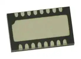
- No. of Pins: 16Pins
- Product Range: -
- Filter Circuit: C-R-C Pi Filter
- EMI Filter Type: EMI Filter with ESD Protection
- No. of Data Lines: 8 Data Lines
- Filter Case / Package: DFN
| Delivery and price | |
|---|---|
| Units per pack | 500 |
| Price | 0.304 € |
| Current stock | 1000+ |
| Lead time | 30 days |
## NUF8410MN

## 8-Channel EMI Filter with Integrated ESD Protection

The NUF8410MN is an eight−channel (C−R−C) Pi−style EMI filter array with integrated ESD protection. Its typical component values of R = 100  and C = 8.5 pF deliver a cutoff frequency of 250 MHz and Q stop band attenuation greater than −20 dB from 800 MHz to 3.0 GHz.

## **http://onsemi.com**

This performance makes the part ideal for parallel interfaces with data rates up to 167 Mbps in applications where wireless interference must be minimized. The specified attenuation range is very effective in minimizing interference from 2G/3G, GPS, Bluetooth® and WLAN signals.

**==> picture [164 x 137] intentionally omitted <==**

**----- Start of picture text -----**<br>
MARKING<br>DIAGRAM<br>16 DFN16 840<br>AYW<br>CASE 506AC<br>1<br>840 = Specific Device Code<br>A = Assembly Location<br>Y = Year<br>W = Work Week<br>= Pb−Free Package<br>(*Note: Microdot may be in either location)<br>**----- End of picture text -----**<br>


The NUF8410MN is available in the low−profile 16−lead 1.6 mm x 4.0 mm DFN16 surface mount package.

## **Features/Benefits**

- ±8.0 kV ESD Protection on each channel (IEC61000−4−2 Level 4, Contact Discharge)

- R/C Values of 100  and 8.5 pF deliver Exceptional S21 0 (*Note: Microdot may be in either location)

- Performance Characteristics of 250 MHz f3dB and −20 dB Stop Band Attenuation from 800 MHz to 3.0 GHz *Date Code orientation and/or position may

   - *Date Code orientation and/or position may vary depending upon manufacturing location.

- Integrated EMI/ESD System Solution in DFN Package Offers Exceptional Cost, System Reliability and Space Savings

## **ORDERING INFORMATION**

- This is a Pb−Free Device

|**Device**|**Package**|**Shipping**†|
|---|---|---|
|NUF8410MNT4G|DFN16<br>(Pb−Free)|4000 / Tape & Reel|


## **Applications**

- EMI Filtering for LCD and Camera Data Lines

   - †For information on tape and reel specifications, including part orientation and tape sizes, please refer to our Tape and Reel Packaging Specifications

- EMI Filtering and Protection for I/O Ports and Keypads

Brochure, BRD8011/D.

**==> picture [229 x 86] intentionally omitted <==**

**----- Start of picture text -----**<br>
Filter + ESDn R = 100  0° Filter + ESDn<br>Cd = 8.5 pFCd = 8.5 pF<br>PS as \<br>ToT Tt<br>See Table 1 for pin description<br>**----- End of picture text -----**<br>


**Figure 1. Electrical Schematic**

**==> picture [246 x 172] intentionally omitted <==**

**----- Start of picture text -----**<br>
0<br>−5<br>−10<br>−15 PTETPL TUTTI aN I ETT<br>−20 ELATIE, ENUT<br>−25<br>UIen AEee EINa EU<br>−30 PL LATTE, ETN<br>−35<br>PEEL EEUUCETLEH<br>−40−45 PEETTT LTE E  ELHET ATTPA<br>1.0E+6 1.0E+7 1.0E+8 1.0E+9 1.0E+10<br>FREQUENCY  (Hz)<br>S21 (dB)<br>**----- End of picture text -----**<br>


**Figure 2. Insertion Loss Characteristic**

Publication Order Number: **NUF84100MN/D**

**1**

© Semiconductor Components Industries, LLC, 2013 **September, 2013 − Rev. 2**

## **NUF8410MN**

**==> picture [176 x 100] intentionally omitted <==**

**----- Start of picture text -----**<br>
1 2 3 4 5 6 7 8<br>GND<br>16 15 14 13 12 11 10 9<br>(Bottom View)<br>**----- End of picture text -----**<br>


**Figure 3. Pin Diagram**

## **Table 1. FUNCTIONAL PIN DESCRIPTION**

|**Table 1. FUNCTIONAL PIN**|**DESCRIPTION**||
|---|---|---|
|**Filter**|**Device Pins**|**Description**|
|Filter 1|1 & 16|Filter + ESD Channel 1|
|Filter 2|2 & 15|Filter + ESD Channel 2|
|Filter 3|3 & 14|Filter + ESD Channel 3|
|Filter 4|4 & 13|Filter + ESD Channel 4|
|Filter 5|5 & 12|Filter + ESD Channel 5|
|Filter 6|6 & 11|Filter + ESD Channel 6|
|Filter 7|7 & 10|Filter + ESD Channel 7|
|Filter 8|8 & 9|Filter + ESD Channel 8|
|Ground Pad|GND|Ground|


## **MAXIMUM RATINGS**

|**MAXIMUM RATINGS**||||
|---|---|---|---|
|**Parameter**|**Symbol**|**Value**|**Unit**|
|ESD Discharge IEC61000−4−2<br>Contact Discharge|VPP|8.0|kV|
|Operating Temperature Range|TOP|−40 to 85|°C|
|Storage Temperature Range|TSTG|−55 to 150|°C|
|Maximum Lead Temperature for Soldering Purposes (1.8 in from case for 10 seconds)|TL|260|°C|


Stresses exceeding Maximum Ratings may damage the device. Maximum Ratings are stress ratings only. Functional operation above the Recommended Operating Conditions is not implied. Extended exposure to stresses above the Recommended Operating Conditions may affect device reliability.

**ELECTRICAL CHARACTERISTICS** (TJ = 25 ° C unless otherwise noted)

|**ELECTRICAL CHARACTERISTICS**|(TJ= 25°C u|nless otherwise noted)|||||
|---|---|---|---|---|---|---|
|**Parameter**|**Symbol**|**Test Conditions**|**Min**|**Typ**|**Max**|**Unit**|
|Maximum Reverse Working Voltage|VRWM||||5.0|V|
|Breakdown Voltage|VBR|IR= 1.0 mA|6.0|7.0|8.0|V|
|Leakage Current|IR|VRWM= 3.3 V|||100|nA|
|Resistance|RA|IR= 20 mA|85|100|115|�|
|Diode Capacitance|Cd|VR= 2.5 V, f = 1.0 MHz||8.5|11|pF|
|Line Capacitance|CL|VR= 2.5 V, f = 1.0 MHz||17|22|pF|
|3 dB Cut−Off Frequency (Note 1)|f3dB|Above this frequency,<br>appreciable attenuation occurs||250||MHz|
|6 dB Cut−Off Frequency|f6dB|Above this frequency,<br>appreciable attenuation occurs||395||MHz|


1. 50 � source and 50 � load termination.

**http://onsemi.com**

**2**

**NUF8410MN**

**TYPICAL PERFORMANCE CURVES** (TA= 25 ° C unless otherwise specified)

**==> picture [251 x 172] intentionally omitted <==**

**----- Start of picture text -----**<br>
0<br>−5<br>−10<br>−15<br>−20<br>−25<br>−30<br>−35<br>−40<br>−45<br>1.0E+6 1.0E+7 1.0E+8 1.0E+9 1.0E+10<br>FREQUENCY  (Hz)<br>S21 (dB)<br>**----- End of picture text -----**<br>


**Figure 4. Insertion Loss Characteristic**

**==> picture [490 x 191] intentionally omitted <==**

**----- Start of picture text -----**<br>
1.6 110<br>108<br>1.4<br>106<br>1.2<br>104<br>1.0<br>102<br>0.8 100<br>98<br>0.6<br>96<br>0.4<br>94<br>0.2 92<br>0 90<br>0 1.0 2.0 3.0 4.0 5.0 −40 −20 0 20 40 60 80<br>REVERSE VOLTAGE (V) TEMPERATURE ( ° C)<br>Figure 5. Typical Capacitance Figure 6. Typical Resistance over Temperature<br>) �<br>RESISTANCE (<br>NORMALIZED CAPACITANCE<br>**----- End of picture text -----**<br>


**http://onsemi.com**

**3**

**NUF8410MN**

## **Theory of Operation**

The NUF8410MN combines ESD protection and EMI filtering conveniently into a small package for today’s size constrained applications. The capacitance inherent to a typical protection diode is utilized to provide the capacitance value necessary to create the desired frequency response based upon the series resistance in the filter. By combining this functionality into one device, a large number of discrete components are integrated into one small package saving valuable board space and reducing BOM count and cost in the application.

## **Application Example**

The accepted practice for specifying bandwidth in a filter is to use the 3 dB cutoff frequency. Utilizing points such as the 6 dB or 9 dB cutoff frequencies results in signal degradation in an application. This can be illustrated in an application example. A typical application would include EMI filtering of data lines in a camera or display interface. In such an example it is important to first understand the signal and its spectral content. By understanding these things, an appropriate filter can be selected for the desired application. A typical data signal is pattern of 1’s and 0’s transmitted over a line in a form similar to a square wave. The maximum frequency of such a signal would be the pattern 1-0-1-0 such that for a signal with a data rate of 100 Mbps, the maximum frequency component would be 50 MHz. The next item to consider is the spectral content of the signal, which can be understood with the Fourier series

approximation of a square wave, shown below in Equations 1 and 2 in the Fourier series approximation.

From this it can be seen that a square wave consists of odd order harmonics and to fully construct a square wave n must go to infinity. However, to retain an acceptable portion of the waveform, the first two terms are generally sufficient. These two terms contain about 85% of the signal amplitude and allow a reasonable square wave to be reconstructed. Therefore, to reasonably pass a square wave of frequency _x_ the minimum filter bandwidth necessary is _3x_ . All ON Semiconductor EMI filters are rated according to this principle. Attempting to violate this principle will result in significant rounding of the waveform and cause problems in transmitting the correct data. For example, take the filter with the response shown in Figure 7 and apply three different data waveforms. To calculate these three different frequencies, the 3 dB, 6 dB, and 9 dB bandwidths will be used.

## **Equation 1:**

**==> picture [211 x 27] intentionally omitted <==**

## **Equation 2 (simplified form of Equation 1):**

**==> picture [232 x 27] intentionally omitted <==**

**==> picture [369 x 181] intentionally omitted <==**

**----- Start of picture text -----**<br>
−3 dB<br>−6 dB<br>−9 dB<br>f1<br>f2<br>f3<br>100k 1M 10M 100M 1G 10G<br>Frequency (Hz)<br>Magnitude (dB)<br>**----- End of picture text -----**<br>


**Figure 7. Filter Bandwidth**

From the above paragraphs it is shown that the maximum supported frequency of a waveform that can be passed through the filter can be found by dividing the bandwidth by a factor of three (to obtain the corresponding data rate

multiply the result by two). The following table gives the bandwidth values and the corresponding maximum supported frequencies and the third harmonic frequencies.

**http://onsemi.com**

**4**

**NUF8410MN**

**Table 2. Frequency Chart**

|**Bandwidth**|**Maximum Supported**<br>**Frequency**|**Third Harmonic**<br>**Frequency**|
|---|---|---|
|3 dB –<br>100 MHz|33.33 MHz (f1)|100 MHz|
|6 dB –<br>200 MHz|66.67 MHz (f2)|200 MHz|
|9 dB –<br>300 MHz|100 MHz (f3)|300 MHz|


Considering that 85% of the amplitude of the square is in the first two terms of the Fourier series approximation most of the signal content is at the fundamental (maximum supported) frequency and the third harmonic frequency. If a signal with a frequency of 33.33 MHz is input to this filter, the first two terms are sufficiently passed such that the signal is only mildly affected, as is shown in Figure 8a. If a signal

with a frequency of 66.67 MHz is input to this same filter, the third harmonic term is significantly attenuated. This serves to round the signal edges and skew the waveform, as is shown in Figure 8b. In the case that a 100 MHz signal is input to this filter, the third harmonic term is attenuated even further and results in even more rounding of the signal edges as is shown in Figure 8c. The result is the degradation of the data being transmitted making the digital data (1’s and 0’s) more difficult to discern. This does not include effects of other components such as interconnect and other path losses which could further serve to degrade the signal integrity. While some filter products may specify the 6 dB or 9 dB bandwidths, actually using these to calculate supported frequencies (and corresponding data rates) results in significant signal degradation. _To ensure the best signal integrity possible, it is best to use the 3 dB bandwidth to calculate the achievable data rate._

**Input Waveform**

**Output Waveform**

**a) Frequency = f1**

**Input Waveform**

**Output Waveform**

**b) Frequency = f2**

**Input Waveform**

**Output Waveform**

**c) Frequency = f3**

**Figure 8. Input and Output Waveforms of Filter**

**http://onsemi.com**

**5**

**NUF8410MN**

## **PACKAGE DIMENSIONS**

**==> picture [459 x 371] intentionally omitted <==**

**----- Start of picture text -----**<br>
DFN16, 4x1.6, 0.5P<br>CASE 506AC<br>ISSUE D<br>D A NOTES:<br>1. DIMENSIONING AND TOLERANCING PER<br>B ANSI Y14.5M, 1982.<br>2. CONTROLLING DIMENSION: MILLIMETER.<br>3. DIMENSION b APPLIES TO TERMINAL AND<br>IS MEASURED BETWEEN 0.25 AND 0.30 MM<br>REFERENCEPIN ONE FROM TERMINAL.<br>2X E 4. COPLANARITY APPLIES TO THE EXPOSED<br>PAD AS WELL AS THE TERMINALS.<br>0.15 C<br>MILLIMETERS<br>S 2X S (A3) iH DIM MIN MAX<br>0.15 C TOP VIEW A 0.80 1.00<br>a C A1 0.00 0.05<br>A3 0.20 REF<br>0.10 C (A3) L Db 0.184.00 BSC0.30<br>D2 3.10 3.30<br>A L1 E 1.60 BSC<br>16X E2 0.30 0.50<br>0.08 C SEATINGPLANE DETAIL AOPTIONAL Ke 0.200.50 BSC−−−<br>lo l SIDE VIEW A1 t iT C CONSTRUCTION ot a L1L 0.200.00 0.400.15<br>RECOMMENDED<br>D2<br>DETAIL A SOLDERING FOOTPRINT*<br>16X L e 2X<br>1 8 0.25 x 0.40 mm 4.10<br>TEST PAD SIZE<br>0.50 PITCH<br>E2<br>16X wu K 16 16X b9 0.10 C A B noono b b ay<br>NOTE 3<br>BOTTOM VIEW —H 0.05 C — 0.50 ooogogog at 1.91<br>16X 0.28 fh 16X 0.51 4 |<br>DIMENSION: MILLIMETERS<br>**----- End of picture text -----**<br>


2. CONTROLLING DIMENSION: MILLIMETER. 3. DIMENSION b APPLIES TO TERMINAL AND IS MEASURED BETWEEN 0.25 AND 0.30 MM FROM TERMINAL.

*For additional information on our Pb−Free strategy and soldering details, please download the ON Semiconductor Soldering and Mounting Techniques Reference Manual, SOLDERRM/D.

Bluetooth is a registered trademark of Bluetooth SIG.

**ON Semiconductor** and          are registered trademarks of Semiconductor Components Industries, LLC (SCILLC).  SCILLC owns the rights to a number of patents, trademarks, copyrights, trade secrets, and other intellectual property. A listing of SCILLC’s product/patent coverage may be accessed at www.onsemi.com/site/pdf/Patent−Marking.pdf.  SCILLC reserves the right to make changes without further notice to any products herein.  SCILLC makes no warranty, representation or guarantee regarding the suitability of its products for any particular purpose, nor does SCILLC assume any liability arising out of the application or use of any product or circuit, and specifically disclaims any and all liability, including without limitation special, consequential or incidental damages.  “Typical” parameters which may be provided in SCILLC data sheets and/or specifications can and do vary in different applications and actual performance may vary over time.  All operating parameters, including “Typicals” must be validated for each customer application by customer’s technical experts.  SCILLC does not convey any license under its patent rights nor the rights of others.  SCILLC products are not designed, intended, or authorized for use as components in systems intended for surgical implant into the body, or other applications intended to support or sustain life, or for any other application in which the failure of the SCILLC product could create a situation where personal injury or death may occur.  Should Buyer purchase or use SCILLC products for any such unintended or unauthorized application, Buyer shall indemnify and hold SCILLC and its officers, employees, subsidiaries, affiliates, and distributors harmless against all claims, costs, damages, and expenses, and reasonable attorney fees arising out of, directly or indirectly, any claim of personal injury or death associated with such unintended or unauthorized use, even if such claim alleges that SCILLC was negligent regarding the design or manufacture of the part.  SCILLC is an Equal Opportunity/Affirmative Action Employer.  This literature is subject to all applicable copyright laws and is not for resale in any manner.

## **PUBLICATION ORDERING INFORMATION**

**N. American Technical Support** : 800−282−9855 Toll Free **ON Semiconductor Website** : **www.onsemi.com** USA/Canada

## **LITERATURE FULFILLMENT** :

Literature Distribution Center for ON Semiconductor USA/Canada P.O. Box 5163, Denver, Colorado 80217 USA **Europe, Middle East and Africa Technical Support: Phone** : 303−675−2175 or 800−344−3860 Toll Free USA/Canada Phone: 421 33 790 2910 **Fax** : 303−675−2176 or 800−344−3867 Toll Free USA/Canada **Japan Customer Focus Center Email** : orderlit@onsemi.com Phone: 81−3−5817−1050

**Order Literature** : http://www.onsemi.com/orderlit For additional information, please contact your local Sales Representative

**http://onsemi.com**

**NUF8410MN/D**

**6**
Updated at April 28, 2026
onsemi is a premier global supplier of intelligent power and sensing technologies, driving disruptive innovations across the automotive, industrial, and cloud infrastructure markets. Recognized for their commitment to sustainability and reliable supply chains, the company accelerates advancements in vehicle electrification, industrial automation, and 5G networks by solving the industry's most complex design challenges. At the core of their portfolio is an industry-leading selection of discrete semiconductors. This extensive range features thousands of high-performance bipolar transistors, single and dual MOSFETs, and a comprehensive array of diodes, including Zener, Schottky, and fast-recovery rectifiers. Engineered for superior thermal performance and energy efficiency, these foundational components are critical for demanding power conversion, switching, and signal conditioning applications. Beyond essential discretes, onsemi provides a robust suite of advanced power management and circuit protection solutions. Their lineup includes intelligent power modules, single IGBTs, and transient voltage suppression (TVS) diodes designed to safeguard sensitive circuitry. Complimented by integrated passive filters, AC/DC LED driver ICs, and specialized sub-2.4GHz RF transceivers, onsemi equips engineers with the scalable, high-quality technologies needed to build a cleaner, smarter, and more connected world.
About Novapart
Novapart is a B2B electronic component broker specialising in stock shortages and cost reduction. We source hard-to-find parts and identify compliant alternatives across a catalogue of 410,000+ components from 500+ manufacturers.
Learn more →Stock Shortage Specialist
When a component is unavailable, discontinued or has an unacceptable lead time, we tap into our network of vetted European and Asian distributors to source what you need — without compromising on quality or traceability.
Request a quote →Compliant Alternatives
We identify pin-to-pin, electrically equivalent substitutes that meet the same certifications (RoHS, AEC-Q100, REACH) as your original specification — validated against datasheets, not just part numbers. Often at a lower cost.
BOM Analysis service →