


NUF2114MNT1G
EMI Filter, 2-Channel, ESD Protection, 50 MHz, DFN-8
- Manufacturer: ONSEMI
- Product type: Integrated Passive Filters
- EMI Filter Type:EMI Filter with ESD Protection; No. of Data Lines:2 Data Lines; Filter Circuit:C-R-C Pi Filter; Filter Case Style:DFN; No. of Pins:8Pins; Product Range:-; SVHC:No SV
- SVHC: No SVHC (25-Jun-2025)
- No. of Pins: 8Pins
- Product Range: -
- Filter Circuit: C-R-C Pi Filter
- EMI Filter Type: EMI Filter with ESD Protection
- No. of Data Lines: 2 Data Lines
- Filter Case / Package: DFN
| Delivery and price | |
|---|---|
| Units per pack | 500 |
| Price | 0.413 € |
| Current stock | 200+ |
| Lead time | 30 days |
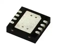
## NUF2114

## 2 Line Audio EMI Filter with ESD Protection

This device is a 2 line audio EMI filter array designed for speaker applications. It offers greater than −30 dB attenuation at frequencies from 900 MHz to 3.0 GHz. This device also offers ESD protection−clamping transients from static discharges and ESD protection is provided across all capacitors.

## **Features**

- Provides EMI Filtering and ESD Protection

- Integration of 10 Discretes

- Compliance with IEC61000−4−2 (Level 4) 30 kV (Contact)

## **http://onsemi.com**

**==> picture [225 x 83] intentionally omitted <==**

**----- Start of picture text -----**<br>
R<br>1 8<br>C C<br>k==:<br>R<br>4 5<br>C C<br>k= = é<br>**----- End of picture text -----**<br>


- DFN8, 2x2 mm Package

- Moisture Sensitivity Level 1

- ESD Ratings: Machine Model = C

   - Human Body Model = 3B

- Matching Series Impedances for Speaker Applications

- This is a Pb−Free Device

## **Applications**

- Wireless Phones

- MP3s

- PDAs

- Digital Cameras

**==> picture [38 x 8] intentionally omitted <==**

**----- Start of picture text -----**<br>
(Top View)<br>**----- End of picture text -----**<br>


**==> picture [171 x 116] intentionally omitted <==**

**----- Start of picture text -----**<br>
MARKING<br>DIAGRAM<br>DFN8 1<br>CASE 506AA U4M<br>&<br>1<br>U4 = Specific Device Code<br>M = Date Code<br>= Pb−Free Package<br>(Note: Microdot may be in either location)<br>**----- End of picture text -----**<br>


- Portable DVDs

## **PIN CONNECTIONS**

**==> picture [138 x 75] intentionally omitted <==**

**----- Start of picture text -----**<br>
OUT1 8 1 IN1<br>NC 7 2 NC<br>GND<br>NC 6 3 NC<br>OUT2 5 4 IN2<br>**----- End of picture text -----**<br>


(Bottom View)

**ORDERING INFORMATION**

> *For additional information on our Pb−Free strategy and soldering details, please download the ON Semiconductor Soldering and Mounting Techniques Reference Manual, SOLDERRM/D.

**Device Package Shipping**[†] NUF2114MNT1G DFN8 3000 / Tape & Reel (Pb−Free) ~~re~~ †For information on tape and reel specifications, including part orientation and tape sizes, please refer to our Tape and Reel Packaging Specification Brochure, BRD8011/D.

Publication Order Number: **NUF2114/D**

**1**

© Semiconductor Components Industries, LLC, 2011 **October, 2011 − Rev. 0**

**NUF2114**

## **MAXIMUM RATINGS**

|**MAXIMUM RATINGS**||||
|---|---|---|---|
|**Parameter**|**Symbol**|**Value**|**Unit**|
|ESD Discharge IEC61000−4−2<br>Contact Discharge|VPP|30|kV|
|Steady−State Power per Resistor @ 25°C|PR|180|mW|
|Steady−State Power per Package @ 25°C|PT|360|mW|
|Operating Temperature Range|TOP|−40 to 85|°C|
|Storage Temperature Range|Tstg|−55 to 150|°C|
|Maximum Lead Temperature for Soldering Purposes (1.8 in from case for 10 s)|TL|260|°C|


Stresses exceeding Maximum Ratings may damage the device. Maximum Ratings are stress ratings only. Functional operation above the Recommended Operating Conditions is not implied. Extended exposure to stresses above the Recommended Operating Conditions may affect device reliability.

## **ELECTRICAL CHARACTERISTICS** (TJ = 25 ° C unless otherwise noted)

|**Parameter**|**Test Conditions**|**Symbol**|**Min**|**Typ**|**Max**|**Unit**|
|---|---|---|---|---|---|---|
|Maximum Reverse Working Voltage||VRWM|−|−|12|V|
|Breakdown Voltage|IR= 1.0 mA|VBR|13.7|15.7|17.7|V|
|Leakage Current|VRWM= 12 V|IR|−|−|0.1|�A|
|Resistance|IF= 40 mA|R|8.1|9.0|9.9|�|
|Capacitance per Diode (Notes 1, 3)||Cd|51|60|66|pF|
|Cut−Off Frequency (Note 2)|Above this frequency,<br>appreciable attenuation occurs|f3dB||50||MHz|


1. Measured at 25 ° C, VR = 0 V, f = 1.0 MHz.

2. 50 � source and 50 � load termination.

3. Total line capacitance is 2 times the diode capacitance (Cd).

**http://onsemi.com**

**2**

**NUF2114**

## **TYPICAL PERFORMANCE CURVES**

(TA = 25 ° C unless otherwise specified)

**==> picture [491 x 391] intentionally omitted <==**

**----- Start of picture text -----**<br>
0 0<br>−5 −10<br>−10<br>−20<br>−15<br>−30<br>−20<br>−40<br>−25<br>−50<br>−30<br>−60<br>−35<br>−40 −70<br>−45 −80<br>1.0E+6 10E+6 100E+6 1.0E+9 10E+9 1.0E+6 10E+6 100E+6 1.0E+9 10E+9<br>FREQUENCY (Hz) FREQUENCY (Hz)<br>Figure 1. Insertion Loss Characteristics Figure 2. Analog Cross−Talk<br>8.7 130<br>120<br>8.6<br>110<br>8.5 100<br>90<br>8.4<br>80<br>8.3 70<br>60<br>8.2<br>50<br>8.1 40<br>−40 −15 10 35 60 85 −12 −8 −4 0 4 8 12<br>TEMPERATURE ( ° C) REVERSE VOLTAGE (VOLTS)<br>(S21) dB (S41) dB<br>CAPACITANCE (pF)<br>RESISTANCE (OHMS)<br>**----- End of picture text -----**<br>


**Figure 3. Typical Resistance over Temperature**

**Figure 4. Typical Line Capacitance vs. Reverse Bias Voltage**

**http://onsemi.com**

**3**

**NUF2114**

## **PACKAGE DIMENSIONS**

**DFN8 2x2, 0.5P** CASE 506AA ISSUE E

**==> picture [483 x 358] intentionally omitted <==**

**----- Start of picture text -----**<br>
D A NOTES:<br>L L 1. DIMENSIONING AND TOLERANCING PER<br>B ASME Y14.5M, 1994 .<br>2. CONTROLLING DIMENSION: MILLIMETERS.<br>L1 3. DIMENSION b APPLIES TO PLATED<br>TERMINAL AND IS MEASURED BETWEEN<br>0.15 AND 0.20 MM FROM TERMINAL TIP.<br>REFERENCEPIN ONE ÇÇÇ m ae E t o f DETAIL AOPTIONAL uf 4. COPLANARITY APPLIES TO THE EXPOSEDPAD AS WELL AS THE TERMINALS.<br>CONSTRUCTIONS<br>2X 0.10 C ÇÇÇ MILLIMETERS<br>DIM MIN MAX<br>ee ÇÇÇ r A 0.80 1.00<br>A1 0.00 0.05<br>2X 0.10 C EXPOSED Cu MOLD CMPD A3 0.20 REF<br>TOP VIEW ÉÉÉ b 0.20 0.30<br>D 2.00 BSC<br>ÉÉÉ D2 1.10 1.30<br>a 0.10 T C DETAIL B A S DETAIL B ey E2E 0.702.00 BSC0.90<br>OPTIONAL e 0.50 BSC<br>CONSTRUCTION K 0.30 REF<br>L 0.25 0.35<br>0.08 C (A3) L1 −−− 0.10<br>a NOTE 4 SIDE VIEW A1 C SEATINGPLANE RECOMMENDED<br>SOLDERING FOOTPRINT*<br>DETAIL A 8X<br>D2 1.30 0.50<br>8X L PACKAGE<br>1 4 OUTLINE<br>E2<br>0.90 2.30<br>K 8 5<br>8X b 1<br>e/2<br>e 0.10 C A B 0.308X 0.50<br>0.05 C NOTE 3 PITCH<br>aif oo m d“ a e k<br>BOTTOM VIEW DIMENSIONS: MILLIMETERS<br>*For additional information on our Pb−Free strategy and soldering<br>details, please download the ON Semiconductor Soldering and<br>Mounting Techniques Reference Manual, SOLDERRM/D.<br>**----- End of picture text -----**<br>


**ON Semiconductor** and          are registered trademarks of Semiconductor Components Industries, LLC (SCILLC).  SCILLC reserves the right to make changes without further notice to any products herein.  SCILLC makes no warranty, representation or guarantee regarding the suitability of its products for any particular purpose, nor does SCILLC assume any liability arising out of the application or use of any product or circuit, and specifically disclaims any and all liability, including without limitation special, consequential or incidental damages. “Typical” parameters which may be provided in SCILLC data sheets and/or specifications can and do vary in different applications and actual performance may vary over time.  All operating parameters, including “Typicals” must be validated for each customer application by customer’s technical experts.  SCILLC does not convey any license under its patent rights nor the rights of others.  SCILLC products are not designed, intended, or authorized for use as components in systems intended for surgical implant into the body, or other applications intended to support or sustain life, or for any other application in which the failure of the SCILLC product could create a situation where personal injury or death may occur.  Should Buyer purchase or use SCILLC products for any such unintended or unauthorized application, Buyer shall indemnify and hold SCILLC and its officers, employees, subsidiaries, affiliates, and distributors harmless against all claims, costs, damages, and expenses, and reasonable attorney fees arising out of, directly or indirectly, any claim of personal injury or death associated with such unintended or unauthorized use, even if such claim alleges that SCILLC was negligent regarding the design or manufacture of the part.  SCILLC is an Equal Opportunity/Affirmative Action Employer.  This literature is subject to all applicable copyright laws and is not for resale in any manner.

## **PUBLICATION ORDERING INFORMATION**

**LITERATURE FULFILLMENT** : **N. American Technical Support** : 800−282−9855 Toll Free **ON Semiconductor Website** : **www.onsemi.com** Literature Distribution Center for ON Semiconductor USA/Canada P.O. Box 5163, Denver, Colorado 80217 USA **Europe, Middle East and Africa Technical Support: Order Literature** : http://www.onsemi.com/orderlit **Phone** : 303−675−2175 or 800−344−3860 Toll Free USA/Canada Phone: 421 33 790 2910 **Fax** : 303−675−2176 or 800−344−3867 Toll Free USA/Canada **Japan Customer Focus Center** For additional information, please contact your local **Email** : orderlit@onsemi.com Phone: 81−3−5817−1050 Sales Representative

## **LITERATURE FULFILLMENT** :

**NUF2114/D**

**http://onsemi.com 4**
Updated at April 28, 2026
onsemi is a premier global supplier of intelligent power and sensing technologies, driving disruptive innovations across the automotive, industrial, and cloud infrastructure markets. Recognized for their commitment to sustainability and reliable supply chains, the company accelerates advancements in vehicle electrification, industrial automation, and 5G networks by solving the industry's most complex design challenges. At the core of their portfolio is an industry-leading selection of discrete semiconductors. This extensive range features thousands of high-performance bipolar transistors, single and dual MOSFETs, and a comprehensive array of diodes, including Zener, Schottky, and fast-recovery rectifiers. Engineered for superior thermal performance and energy efficiency, these foundational components are critical for demanding power conversion, switching, and signal conditioning applications. Beyond essential discretes, onsemi provides a robust suite of advanced power management and circuit protection solutions. Their lineup includes intelligent power modules, single IGBTs, and transient voltage suppression (TVS) diodes designed to safeguard sensitive circuitry. Complimented by integrated passive filters, AC/DC LED driver ICs, and specialized sub-2.4GHz RF transceivers, onsemi equips engineers with the scalable, high-quality technologies needed to build a cleaner, smarter, and more connected world.
About Novapart
Novapart is a B2B electronic component broker specialising in stock shortages and cost reduction. We source hard-to-find parts and identify compliant alternatives across a catalogue of 410,000+ components from 500+ manufacturers.
Learn more →Stock Shortage Specialist
When a component is unavailable, discontinued or has an unacceptable lead time, we tap into our network of vetted European and Asian distributors to source what you need — without compromising on quality or traceability.
Request a quote →Compliant Alternatives
We identify pin-to-pin, electrically equivalent substitutes that meet the same certifications (RoHS, AEC-Q100, REACH) as your original specification — validated against datasheets, not just part numbers. Often at a lower cost.
BOM Analysis service →