
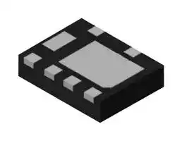


NSPU5132MUTBG
TVS Diode, Unidirectional, 13.5 V, 24 V, UDFN, 6 Pins
- Manufacturer: ONSEMI
- Product type: TVS Diodes
- Product Range:-; TVS Polarity:Unidirectional; Reverse Stand-Off Voltage Vrwm:13.5V; Clamping Voltage Vc Max:24V; Diode Case Style:UDFN; No. of Pins:6Pins; Breakdown Voltage Min:13.6
- SVHC: No SVHC (25-Jun-2025)
- No. of Pins: 6Pins
- TVS Polarity: Unidirectional
- Product Range: -
- Qualification: -
- Diode Mounting: Surface Mount
- Diode Case Style: UDFN
- Clamping Voltage Max: 24V
- Reverse Standoff Voltage: 13.5V
- Maximum Breakdown Voltage: 17.5V
- Minimum Breakdown Voltage: 13.6V
- Operating Temperature Max: 125°C
- Peak Pulse Power Dissipation: 4.8kW
| Delivery and price | |
|---|---|
| Units per pack | 1000 |
| Price | 0.126 € |
| Current stock | 1000+ |
| Lead time | 30 days |
## NSPU5132

## 13.5 V Unidirectional ESD and Surge Protection Device

## **Features**

- Unidirectional High Voltage ESD & Surge Protection Device

- Provides ESD Protection to IEC61000−4−2 Level 4:

## **www.onsemi.com**

   - ±30 kV Contact Discharge

- Small Package (1.8 mm x 2.0 mm)

- High Voltage Zener Diode Protects Supply Rail up to 200 A (8/20 s)

- These Devices are Pb−Free and are RoHS Compliant

**==> picture [50 x 26] intentionally omitted <==**

**----- Start of picture text -----**<br>
UDFN6<br>D4 SUFFIX<br>CASE 517CS<br>**----- End of picture text -----**<br>


## **APPLICATION DIAGRAM**

**==> picture [195 x 198] intentionally omitted <==**

**----- Start of picture text -----**<br>
Vcc (1,2,3,4)<br>GND (6,8)<br>DAP**<br>GND (5,7)<br>**Die Attach Pad on<br>|! 7<br>back of package<br>(connect to ground)<br>**----- End of picture text -----**<br>


## **BLOCK DIAGRAM**

**==> picture [142 x 7] intentionally omitted <==**

**----- Start of picture text -----**<br>
Cathode Anode<br>**----- End of picture text -----**<br>


## **MARKING DIAGRAM**

**==> picture [297 x 133] intentionally omitted <==**

**----- Start of picture text -----**<br>
4W M<br>1<br>4W = Specific Device Code<br>M = Date Code<br>= Pb−Free Package<br>ORDERING INFORMATION<br>Device Package Shipping [†]<br>NSPU5132MUTBG UDFN6 3000 / Tape &<br>(Pb−Free) Reel<br>"ESF<br>**----- End of picture text -----**<br>


†For information on tape and reel specifications, including part orientation and tape sizes, please refer to our Tape and Reel Packaging Specification Brochure, BRD8011/D.

Publication Order Number:

**1**

© Semiconductor Components Industries, LLC, 2017 **November, 2018 − Rev. 1**

**NSPU5132/D**

**NSPU5132**

## **Table 1. PIN DESCRIPTIONS**

|**Table 1. PIN DESCRIPTIONS**|**Table 1. PIN DESCRIPTIONS**|**Table 1. PIN DESCRIPTIONS**|
|---|---|---|
||||
|||**6−Lead, UDFN−8 Package**|
|**Pin**|**Name**|**Description**|
|1|VCC|Cathode|
|2|VCC|Cathode|
|3|VCC|Cathode|
|4|VCC|Cathode|
|5|GND|Anode|
|6|GND|Anode|
|7|GND|Anode|
|8|GND|Anode|


## **PACKAGE / PINOUT DIAGRAMS**

**==> picture [212 x 117] intentionally omitted <==**

**----- Start of picture text -----**<br>
Top View Bottom View<br>(Pins Down View) (Pins Up View)<br>6   5 1 2 3 4<br>XX M 8 7<br>Pin 1<br>Marking<br>1   2   3   4 6 5<br>6−Lead UDFN<br>**----- End of picture text -----**<br>


## **ELECTRICAL CHARACTERISTICS**

|**Symbol**|**Parameter**|
|---|---|
|IPP|Maximum Reverse Peak Pulse Current|
|VC|Clamping Voltage @ IPP|
|VRWM|Working Peak Reverse Voltage|
|IR|Maximum Reverse Leakage Current @ VRWM|
|VBR|Breakdown Voltage @ IT|
|IT|Test Current|
|�VBR|Maximum Temperature Coefficient of VBR|
|IF|Forward Current|
|VF|Forward Voltage @ IF|


**==> picture [195 x 180] intentionally omitted <==**

**----- Start of picture text -----**<br>
I<br>IF<br>VC VBR VRWM<br>V<br>IR VF<br>IT<br>IPP<br>Uni−Directional Surge Protection<br>**----- End of picture text -----**<br>


## **SPECIFICATIONS**

## **Table 2. ABSOLUTE MAXIMUM RATINGS**

|**Table 2. ABSOLUTE MAXIMUM RATINGS**|||
|---|---|---|
|**Parameter**|**Rating**|**Units**|
|Operating Temperature Range|–55 to +125|°C|
|Storage Temperature Range|–65 to +150|°C|
|Peak Current (tp= 8/20�s)|200|A|
|Peak Pulse Power (tp= 8/20�s)|4800|W|


Stresses exceeding those listed in the Maximum Ratings table may damage the device. If any of these limits are exceeded, device functionality should not be assumed, damage may occur and reliability may be affected.

## **ELECTRICAL CHARACTERISTICS**

|**Device**<br>**Name**|**Device**<br>**Marking**|**VRWM (V)**<br>(Note 1)|**IR @ VRWM**<br>**��A)**|**Breakdown Voltage**|**Breakdown Voltage**|**Breakdown Voltage**|**Breakdown Voltage**|**VC @ IPP**<br>(8 x 20�s) (Note 3)|**VC @ IPP**<br>(8 x 20�s) (Note 3)|**Junction Capacitance**<br>(VR= 0 V, f = 1 MHz,<br>Pin 1 to Pin 5)|**Junction Capacitance**<br>(VR= 0 V, f = 1 MHz,<br>Pin 1 to Pin 5)|
|---|---|---|---|---|---|---|---|---|---|---|---|
|||||**VBRV **(Note 2)|||**@ IT (mA)**|**VC (V)**|**IPP (A)**|**CJ (**|**pF)**|
|||**Max**|**Max**|**Min**|**Nom**|**Max**||**Max**||**Typ**|**Max**|
|NSPU5132|4W|13.5|0.5|13.6|15.5|17.5|1|24|200|1325|1550|


Product parametric performance is indicated in the Electrical Characteristics for the listed test conditions, unless otherwise noted. Product performance may not be indicated by the Electrical Characteristics if operated under different conditions.

1. A surge protector is normally selected according to the working peak reverse voltage (VRWM), which should be equal to or greater than the DC or continuous peak operating voltage level.

2. VBR measured at pulse test current IT at an ambient temperature of 25 ° C.

3. Surge current waveform per Figure 1.

**www.onsemi.com**

**2**

**NSPU5132**

## **TYPICAL CHARACTERISTICS**

**==> picture [234 x 168] intentionally omitted <==**

**----- Start of picture text -----**<br>
tr = rise time to peak value [8  � s]<br>Peak tf = decay time to half value [20  � s]<br>100<br>Value<br>50 Half Value<br>0<br>0 tr tf<br>TIME ( � s)<br>Ipp - PEAK PULSE CURRENT - %Ipp<br>**----- End of picture text -----**<br>


**Figure 1. IEC61000−4−5 8/20 � s Pulse Waveform**

**==> picture [235 x 171] intentionally omitted <==**

**----- Start of picture text -----**<br>
24<br>22<br>20<br>18<br>16<br>14<br>12<br>10<br>8<br>6<br>4<br>2<br>0<br>0 20 40 60 80 100 120 140 160 180 200 220 240<br>IPK (A)<br> (V)<br>PK<br> @ I<br>C<br>V<br>**----- End of picture text -----**<br>


**Figure 2. Positive Clamping Voltage vs. Peak Pulse Current**

**www.onsemi.com**

**3**

MECHANICAL CASE OUTLINE **PACKAGE DIMENSIONS**

**UDFN6, 1.8x2, 0.4P** CASE 517CS ISSUE O

## DATE 30 APR 2013

**==> picture [448 x 347] intentionally omitted <==**

**----- Start of picture text -----**<br>
SCALE 4:1<br>D A B EXPOSED Cu MOLD CMPD NOTES:<br>1.<br>ÇÇ Y14.5M, 1994.<br>2.<br>ÇÇÉÉ 3.<br>- a S DETAIL B aw FROM THE TERMINAL TIP.<br>PIN ONE E ALTERNATE 4.<br>REFERENCE CONSTRUCTION AS WELL AS THE TERMINALS.<br>ÍÍÍ<br>MILLIMETERS<br>2X 0.10 C ÍÍÍ DIM MIN MAX<br>at i A 0.45 0.55<br>2X 0.10 ÍÍÍ C TOP VIEW L L A1A3 0.000.125 REF0.05<br>b 0.15 0.25<br>D 1.80 BSC<br>L1 D2 0.35 0.55<br>DETAIL B E 2.00 BSC<br>0.05 C A3 DETAIL AALTERNATE E2e 0.740.40 BSC0.94<br>6X A CONSTRUCTIONS e1 0.80 BSC<br>e2 0.95 BSC<br>0.05 C L 0.20 0.40<br>NOTE 4 ao SIDE VIEW A1 C SEATINGPLANE tof of a L1 --- 0.15<br>GENERIC<br>MARKING DIAGRAM*<br>e/2<br>0.10 C<br>DETAIL A 2X D2 e XX M<br>6X b<br>1 4 1 4 1<br>0.07 C A B<br>ayumi r 2X E2 cal : ro | 0.05 C NOTE 3 XX = Specific Device Code<br>u tt M = Date Code<br>6X L<br>0.10 C<br>Pb−Free indicator, “G” or microdot “ ”,<br>gt 6 5 [i] [o)] 6 5 J may or may not be present.<br>e1/2 e2<br>A y he e1 = SUPPLEMENTAL RECOMMENDED<br>BOTTOM VIEW BOTTOM VIEW MOUNTING FOOTPRINT*<br>**----- End of picture text -----**<br>


1. DIMENSIONING AND TOLERANCING PER ASME Y14.5M, 1994.

2. CONTROLLING DIMENSION: MILLIMETERS.

3. DIMENSION b APPLIES TO PLATED TERMINALS AND IS MEASURED BETWEEN 0.15 AND 0.30mm FROM THE TERMINAL TIP.

4. COPLANARITY APPLIES TO THE EXPOSED PAD

XX M 1 XX = Specific Device Code M = Date Code *This information is generic. Please refer to device data sheet for actual part marking. Pb−Free indicator, “G” or microdot “ ”, . may or may not be present.

**==> picture [226 x 175] intentionally omitted <==**

**----- Start of picture text -----**<br>
0.95<br>0.40<br>PITCH 6X<br>0.48<br>2X 0.55<br>PACKAGE<br>OUTLINE 2X<br>0.94 2.20<br>ie<br>0.40<br>6X 0.25 ‘poa PITCH t<br>DIMENSIONS: MILLIMETERS<br>*For additional information on our Pb−Free strategy and soldering<br>details, please download the ON Semiconductor Soldering and<br>Mounting Techniques Reference Manual, SOLDERRM/D.<br>**----- End of picture text -----**<br>


Electronic versions are uncontrolled except when accessed directly from the Document Repository. **DOCUMENT NUMBER: 98AON89602E** Printed  versions are uncontrolled  except when stamped  “CONTROLLED COPY” in red. **DESCRIPTION: UDFN6 1.8X2, 0.4P PAGE 1 OF 1** ~~es~~ ON Semiconductor and          are trademarks of Semiconductor Components Industries, LLC dba ON Semiconductor or its subsidiaries in the United States and/or other countries. ON Semiconductor reserves the right to make changes without further notice to any products herein. ON Semiconductor makes no warranty, representation or guarantee regarding the suitability of its products for any particular purpose, nor does ON Semiconductor assume any liability arising out of the application or use of any product or circuit, and specifically disclaims any and all liability, including without limitation special, consequential or incidental damages. ON Semiconductor does not convey any license under its patent rights nor the rights of others.

Electronic versions are uncontrolled except when accessed directly from the Document Repository. Printed  versions are uncontrolled  except when stamped  “CONTROLLED COPY” in red.

www.onsemi.com

© Semiconductor Components Industries, LLC, 2019

ON Semiconductor and      are trademarks of Semiconductor Components Industries, LLC dba ON Semiconductor or its subsidiaries in the United States and/or other countries. ON Semiconductor owns the rights to a number of patents, trademarks, copyrights, trade secrets, and other intellectual property. A listing of ON Semiconductor’s product/patent coverage may be accessed at www.onsemi.com/site/pdf/Patent−Marking.pdf. ON Semiconductor reserves the right to make changes without further notice to any products herein. ON Semiconductor makes no warranty, representation or guarantee regarding the suitability of its products for any particular purpose, nor does ON Semiconductor assume any liability arising out of the application or use of any product or circuit, and specifically disclaims any and all liability, including without limitation special, consequential or incidental damages. Buyer is responsible for its products and applications using ON Semiconductor products, including compliance with all laws, regulations and safety requirements or standards, regardless of any support or applications information provided by ON Semiconductor. “Typical” parameters which may be provided in ON Semiconductor data sheets and/or specifications can and do vary in different applications and actual performance may vary over time. All operating parameters, including “Typicals” must be validated for each customer application by customer’s technical experts. ON Semiconductor does not convey any license under its patent rights nor the rights of others. ON Semiconductor products are not designed, intended, or authorized for use as a critical component in life support systems or any FDA Class 3 medical devices or medical devices with a same or similar classification in a foreign jurisdiction or any devices intended for implantation in the human body. Should Buyer purchase or use ON Semiconductor products for any such unintended or unauthorized application, Buyer shall indemnify and hold ON Semiconductor and its officers, employees, subsidiaries, affiliates, and distributors harmless against all claims, costs, damages, and expenses, and reasonable attorney fees arising out of, directly or indirectly, any claim of personal injury or death associated with such unintended or unauthorized use, even if such claim alleges that ON Semiconductor was negligent regarding the design or manufacture of the part. ON Semiconductor is an Equal Opportunity/Affirmative Action Employer. This literature is subject to all applicable copyright laws and is not for resale in any manner.

## **PUBLICATION ORDERING INFORMATION**

**LITERATURE FULFILLMENT** : **TECHNICAL SUPPORT Email Requests to:** orderlit@onsemi.com **North American Technical Support:** Voice Mail: 1 800−282−9855 Toll Free USA/Canada **ON Semiconductor Website:** www.onsemi.com Phone: 011 421 33 790 2910

◊

**www.onsemi.com**

**Europe, Middle East and Africa Technical Support:** Phone: 00421 33 790 2910 For additional information, please contact your local Sales Representative

**1**
Updated at June 1, 2026
onsemi is a premier global supplier of intelligent power and sensing technologies, driving disruptive innovations across the automotive, industrial, and cloud infrastructure markets. Recognized for their commitment to sustainability and reliable supply chains, the company accelerates advancements in vehicle electrification, industrial automation, and 5G networks by solving the industry's most complex design challenges. At the core of their portfolio is an industry-leading selection of discrete semiconductors. This extensive range features thousands of high-performance bipolar transistors, single and dual MOSFETs, and a comprehensive array of diodes, including Zener, Schottky, and fast-recovery rectifiers. Engineered for superior thermal performance and energy efficiency, these foundational components are critical for demanding power conversion, switching, and signal conditioning applications. Beyond essential discretes, onsemi provides a robust suite of advanced power management and circuit protection solutions. Their lineup includes intelligent power modules, single IGBTs, and transient voltage suppression (TVS) diodes designed to safeguard sensitive circuitry. Complimented by integrated passive filters, AC/DC LED driver ICs, and specialized sub-2.4GHz RF transceivers, onsemi equips engineers with the scalable, high-quality technologies needed to build a cleaner, smarter, and more connected world.
About Novapart
Novapart is a B2B electronic component broker specialising in stock shortages and cost reduction. We source hard-to-find parts and identify compliant alternatives across a catalogue of 540,000+ components from 500+ manufacturers.
Learn more →Stock Shortage Specialist
When a component is unavailable, discontinued or has an unacceptable lead time, we tap into our network of vetted European and Asian distributors to source what you need — without compromising on quality or traceability.
Request a quote →Compliant Alternatives
We identify pin-to-pin, electrically equivalent substitutes that meet the same certifications (RoHS, AEC-Q100, REACH) as your original specification — validated against datasheets, not just part numbers. Often at a lower cost.
BOM Analysis service →