


NRVTS360ETFSWFTAG
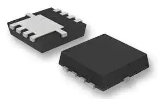
Schottky Rectifier, 60 V, 3 A, Single, WDFN, 8 Pins, 900 mV
- Manufacturer: ONSEMI
- Product type: Schottky Rectifier Diodes
- Diode Mounting: Surface Mount
| Delivery and price | |
|---|---|
| Units per pack | 500 |
| Price | 0.21 € |
| Current stock | 10+ |
| Lead time | 30 days |
## NRVTS360TFS

## Trench Surface Mount Schottky Rectifier

This 8FL flat lead ultrafast rectifier provides fast switching performance with soft recovery in a compact thermally efficient package. Its compact footprint makes it ideally suited to portable and automotive applications where board space is at a premium. Its low profile makes it a good option for flat panel display and other applications with limited vertical clearance. The device offers low leakage over temperature making it a good match for applications requiring low quiescent current.

**www.onsemi.com**

**TRENCH SCHOTTKY RECTIFIER 3.0 AMPERE 60 VOLTS**

## **Features**

- Fast Soft Switching for Reduced EMI and Higher Efficiency

- Low Profile − Maximum Height of 1.1 mm

- Small Footprint − Footprint Area of 13.5 mm[2]

- NRV Prefix for Automotive and Other Applications Requiring Unique Site and Control Change Requirements; AEC−Q101 Qualified and PPAP Capable

- WF in Suffix of Part Number Denotes Wettable Flanks Option for Enhanced Automated Inspection

- These Devices are Pb−Free, Halogen Free/BFR Free and are RoHS Compliant

## **Mechanical Characteristics:**

- Case: Molded Epoxy

- Epoxy Meets UL 94 V−0 @ 0.125 in

- Weight: 95 mg (Approximately)

- Lead and Mounting Surface Temperature for Soldering Purposes: 260°C Maximum for 10 Seconds

- MSL 1

## **Applications**

~~=~~ 1 **WDFN8 ( 8FL) CASE 511AB FLAT LEAD**

## **MARKING DIAGRAM**

**==> picture [115 x 118] intentionally omitted <==**

**----- Start of picture text -----**<br>
1<br>A C<br>A T360 C<br>A AYWW C<br>NC C<br>T360 = Specific Device Code<br>A = Assembly Location<br>Y = Year<br>WW = Work Week<br>= Pb−Free Package<br>**----- End of picture text -----**<br>


(Note: Microdot may be in either location)

- Switching Power Supplies including Mini−adapters and Displays

- Instrumentation

- Engine Control Recirculation Diodes

- Freewheeling Diode Where Space is at a Premium

- Automotive LED Lighting

## **ORDERING INFORMATION**

|**Device**|**Package**|**Shipping**†|
|---|---|---|
|NRVTS360TFSTAG|WDFN8<br>(Pb−Free)|1500 / Tape<br>& Reel|
|NRVTS360TFSWFTAG||1500 / Tape<br>& Reel|


- †For information on tape and reel specifications, including part orientation and tape sizes, please refer to our Tape and Reel Packaging Specification Brochure, BRD8011/D.

Publication Order Number: **NRVTS360TFS/D**

**1**

© Semiconductor Components Industries, LLC, 2016 **September, 2017 − Rev. 1**

**NRVTS360TFS**

## **MAXIMUM RATINGS**

|**MAXIMUM RATINGS**||||
|---|---|---|---|
|**Rating**|**Symbol**|**Value**|**Unit**|
|Peak Repetitive Reverse Voltage<br>Working Peak Reverse Voltage<br>DC Blocking Voltage|VRRM<br>VRWM<br>VR|60|V|
|Average Rectified Forward Current<br>(TL= 163°C)|IO|3.0|A|
|Peak Repetitive Forward Current<br>(Rated VR, Square Wave, 20 kHz) TL= 166°C|IFRM|6.0|A|
|Non−Repetitive Peak Surge Current<br>(Surge Applied at Rated Load Conditions Halfwave, Single Phase, 60 Hz)|IFSM|50|A|
|Storage Temperature Range|Tstg|−65 to +175|°C|
|Operating Junction Temperature|TJ|−65 to +175|°C|


Stresses exceeding those listed in the Maximum Ratings table may damage the device. If any of these limits are exceeded, device functionality should not be assumed, damage may occur and reliability may be affected.

## **THERMAL CHARACTERISTICS**

|**THERMAL CHARACTERISTICS**||||
|---|---|---|---|
|**Characteristic**|**Symbol**|**Value**|**Unit**|
|Thermal Resistance, Junction−to−Tab (Note 1)|�JCT|2.7|°C/W|
|Thermal Resistance, Junction−to−Ambient (Note 1)|R�JA|57.7|°C/W|


1. 1 inch square pad size (1 × 0.5 inch) for each lead on FR4 board.

## **ELECTRICAL CHARACTERISTICS**

|**ELECTRICAL CHARACTERISTICS**|||||
|---|---|---|---|---|
|**Characteristic**|**Symbol**|**Typ**|**Max**|**Unit**|
|Instantaneous Forward Voltage (Note 1)<br>(iF= 3.0 Amps, TJ= 25°C)<br>(iF= 6.0 Amps, TJ= 25°C)<br>(iF= 3.0 Amps, TJ= 125°C)<br>(iF= 6.0 Amps, TJ= 125°C)|vF|0.60<br>0.75<br>0.57<br>0.69|0.70<br>0.90<br>0.65<br>0.77|V|
|Instantaneous Reverse Current (Note 1)<br>(Rated dc Voltage, TJ= 25°C)<br>(Rated dc Voltage, TJ= 125°C)|iR|1.0<br>0.8|12<br>4.0|�A<br>mA|


Product parametric performance is indicated in the Electrical Characteristics for the listed test conditions, unless otherwise noted. Product performance may not be indicated by the Electrical Characteristics if operated under different conditions.

1. Pulse Test: Pulse Width = 300 � s, Duty Cycle ≤ 2.0%.

**www.onsemi.com**

**2**

**NRVTS360TFS**

## **TYPICAL CHARACTERISTICS**

**==> picture [493 x 591] intentionally omitted <==**

**----- Start of picture text -----**<br>
100 100<br>TA = 175 ° C<br>10 10<br>TA = 175 ° C TA = 150 ° C<br>T A  = 150 ° C T A  = 125 ° C<br>1 TA = 125 ° C TA = 85 ° C 1 TA = 85 ° C<br>TA = 25 ° C TA = 25 ° C<br>0.1 TA = −55 ° C 0.1 TA = −55 ° C<br>0.0 0.2 0.4 0.6 0.8 1.0 1.2 0.2 0.4 0.6 0.8 1.0 1.2 1.4<br>VF, INSTANTANEOUS FORWARD VOLTAGE (V) VF, INSTANTANEOUS FORWARD VOLTAGE (V)<br>Figure 1. Typical Instantaneous Forward Figure 2. Maximum Instantaneous Forward<br>Characteristics Characteristics<br>1.E−01 1.E−01<br>TA = 175 ° C<br>1.E−02 TA = 175 ° C 1.E−02 TA = 150 ° C<br>TA = 150 ° C TA = 125 ° C<br>1.E−03 TA = 125 ° C 1.E−03 TA = 85 ° C<br>1.E−04 TA = 85 ° C 1.E−04<br>1.E−05 1.E−05 TA = 25 ° C<br>1.E−06 TA = 25 ° C 1.E−06<br>1.E−07 1.E−07<br>5 10 15 20 25 30 35 40 45 50 55 60 5 10 15 20 25 30 35 40 45 50 55 60<br>VR, INSTANTANEOUS REVERSE VOLTAGE (V) VR, INSTANTANEOUS REVERSE VOLTAGE (V)<br>Figure 3. Typical Reverse Characteristics Figure 4. Maximum Reverse Characteristics<br>1000 6<br>TJ = 25 ° C R � JC = 4.0 ° C/W<br>5 DC<br>4<br>SQUARE WAVE<br>100 3<br>2<br>1<br>10 0<br>0.1 1 10 120 130 140 150 160 170 180<br>VR, REVERSE VOLTAGE (V) TC, CASE TEMPERATURE ( ° C)<br>CURRENT (A) CURRENT (A)<br>, INSTANTANEOUS FORWARD , INSTANTANEOUS FORWARD<br>iF iF<br>, INSTANTANEOUS REVERSE CURRENT (A) , INSTANTANEOUS REVERSE CURRENT (A)<br>IR IR<br>, AVERAGE FORWARD CURRENT (A)<br>C, JUNCTION CAPACITANCE (pF)<br>IF(AV)<br>**----- End of picture text -----**<br>


**Figure 5. Typical Junction Capacitance**

**Figure 6. Current Derating per Diode**

**www.onsemi.com**

**3**

**NRVTS360TFS**

## **TYPICAL CHARACTERISTICS**

**==> picture [241 x 155] intentionally omitted <==**

**----- Start of picture text -----**<br>
14<br>IPK/IAV = 20<br>12<br>IPK/IAV = 10<br>10<br>8<br>6<br>SQUARE WAVE<br>4<br>IPK/IAV = 5<br>2<br>DC<br>0<br>0 1 2 3<br>DISSIPATION (W)<br>, AVERAGE FORWARD POWER<br>F(AV)<br>P<br>**----- End of picture text -----**<br>


IF(AV), AVERAGE FORWARD CURRENT (A)

**Figure 7. Forward Power Dissipation**

**==> picture [490 x 173] intentionally omitted <==**

**----- Start of picture text -----**<br>
10<br>50% (DUTY CYCLE)<br>20%<br>10%<br>1<br>5.0%<br>2.0%<br>1.0%<br>SINGLE PULSE Assumes 25°C ambient and soldered to a 650 mm [2]  - 1 oz copper pad on PCB<br>0.1<br>0.000001 0.00001 0.0001 0.001 0.01 0.1 1.0<br>PULSE TIME (s)<br>R(t) (C/W)<br>**----- End of picture text -----**<br>


**Figure 8. Typical Thermal Characteristics**

**www.onsemi.com**

**4**

**NRVTS360TFS**

## **PACKAGE DIMENSIONS**

**WDFN8 3.3x3.3, 0.65P** CASE 511AB ISSUE D

**==> picture [9 x 5] intentionally omitted <==**

**----- Start of picture text -----**<br>
2X<br>**----- End of picture text -----**<br>


**==> picture [486 x 355] intentionally omitted <==**

**----- Start of picture text -----**<br>
e 0.20 l C NOTES:1. DIMENSIONING AND TOLERANCING PER ASME Y14.5M, 1994.<br>2. CONTROLLING DIMENSION: MILLIMETERS.<br>D A 3. DIMENSION D1 AND E1 DO NOT INCLUDE MOLD FLASH<br>L au n B 2X PROTRUSIONS OR GATE BURRS.<br>D1<br>8 7 6 5 0.20 C DIM MINMILLIMETERSNOM MAX MIN INCHESNOM MAX<br>A 0.70 0.75 0.80 0.028 0.030 0.031<br>4X A1 0.00 −−− 0.05 0.000 −−− 0.002<br>eee E1 E eee b 0.23 0.30 0.40 0.009 0.012 0.016<br>c 0.15 0.20 0.25 0.006 0.008 0.010<br>D 3.30 BSC 0.130 BSC<br>1 2 3 4 c == A1 ===== D1D2 2.951.98 3.052.11 3.152.24 0.0780.116 0.0830.120 0.1240.088<br>TOP VIEW E 3.30 BSC 0.130 BSC<br>E1 2.95 3.05 3.15 0.116 0.120 0.124<br>0.10 C E2 1.47 1.60 1.73 0.058 0.063 0.068<br>E3 0.23 0.30 0.40 0.009 0.012 0.016<br>4 ) PP ===<br>A 6X C Ge 0.30 0.65 BSC0.41 0.51 0.012 0.026 BSC0.016 0.020<br>a 0.10 C <i e SEATINGPLANE == K 0.65 0.80 0.95 0.026 0.032 0.037<br>L 0.30 0.43 0.56 0.012 0.017 0.022<br>SIDE VIEW DETAIL A DETAIL A L1 0.06 0.13 0.20 0.002 0.005 0.008<br>- SSS M 1.40 1.50 1.60  SS= 0.055 0.059 0.063<br>. 0  −−− 12  0  −−− 12<br>8X b<br>0.10 C A B<br>SOLDERING FOOTPRINT*<br>0.05 C<br>8X<br>4X L e/2 0.42 0.65 4X<br>eT 1 4 PITCH 0.66<br>PACKAGE<br>ilo K OUTLINE ae<br>E2 j eu tate<br>E3 M<br>8 R 5 e L1 | 3.60<br>G D2<br>BOTTOM VIEW 0.75 0.57 2.30<br>0.47 2.37<br>3.46<br>DIMENSION: MILLIMETERS<br>**----- End of picture text -----**<br>


*For additional information on our Pb−Free strategy and soldering details, please download the ON Semiconductor Soldering and Mounting Techniques Reference Manual, SOLDERRM/D.

ON Semiconductor and      are trademarks of Semiconductor Components Industries, LLC dba ON Semiconductor or its subsidiaries in the United States and/or other countries. ON Semiconductor owns the rights to a number of patents, trademarks, copyrights, trade secrets, and other intellectual property. A listing of ON Semiconductor’s product/patent coverage may be accessed at www.onsemi.com/site/pdf/Patent−Marking.pdf. ON Semiconductor reserves the right to make changes without further notice to any products herein. ON Semiconductor makes no warranty, representation or guarantee regarding the suitability of its products for any particular purpose, nor does ON Semiconductor assume any liability arising out of the application or use of any product or circuit, and specifically disclaims any and all liability, including without limitation special, consequential or incidental damages. Buyer is responsible for its products and applications using ON Semiconductor products, including compliance with all laws, regulations and safety requirements or standards, regardless of any support or applications information provided by ON Semiconductor. “Typical” parameters which may be provided in ON Semiconductor data sheets and/or specifications can and do vary in different applications and actual performance may vary over time. All operating parameters, including “Typicals” must be validated for each customer application by customer’s technical experts. ON Semiconductor does not convey any license under its patent rights nor the rights of others. ON Semiconductor products are not designed, intended, or authorized for use as a critical component in life support systems or any FDA Class 3 medical devices or medical devices with a same or similar classification in a foreign jurisdiction or any devices intended for implantation in the human body. Should Buyer purchase or use ON Semiconductor products for any such unintended or unauthorized application, Buyer shall indemnify and hold ON Semiconductor and its officers, employees, subsidiaries, affiliates, and distributors harmless against all claims, costs, damages, and expenses, and reasonable attorney fees arising out of, directly or indirectly, any claim of personal injury or death associated with such unintended or unauthorized use, even if such claim alleges that ON Semiconductor was negligent regarding the design or manufacture of the part. ON Semiconductor is an Equal Opportunity/Affirmative Action Employer. This literature is subject to all applicable copyright laws and is not for resale in any manner.

## **PUBLICATION ORDERING INFORMATION**

**LITERATURE FULFILLMENT** : **N. American Technical Support** : 800−282−9855 Toll Free **ON Semiconductor Website** : **www.onsemi.com** Literature Distribution Center for ON Semiconductor USA/Canada 19521 E. 32nd Pkwy, Aurora, Colorado 80011 USA **Europe, Middle East and Africa Technical Support: Order Literature** : http://www.onsemi.com/orderlit **Phone** : 303−675−2175 or 800−344−3860 Toll Free USA/Canada Phone: 421 33 790 2910 **Fax** : 303−675−2176 or 800−344−3867 Toll Free USA/Canada **Japan Customer Focus Center** For additional information, please contact your local **Email** : orderlit@onsemi.com Phone: 81−3−5817−1050 Sales Representative

◊

**www.onsemi.com**

**NRVTS360TFS/D**

**5**
Updated at February 9, 2023
onsemi is a premier global supplier of intelligent power and sensing technologies, driving disruptive innovations across the automotive, industrial, and cloud infrastructure markets. Recognized for their commitment to sustainability and reliable supply chains, the company accelerates advancements in vehicle electrification, industrial automation, and 5G networks by solving the industry's most complex design challenges. At the core of their portfolio is an industry-leading selection of discrete semiconductors. This extensive range features thousands of high-performance bipolar transistors, single and dual MOSFETs, and a comprehensive array of diodes, including Zener, Schottky, and fast-recovery rectifiers. Engineered for superior thermal performance and energy efficiency, these foundational components are critical for demanding power conversion, switching, and signal conditioning applications. Beyond essential discretes, onsemi provides a robust suite of advanced power management and circuit protection solutions. Their lineup includes intelligent power modules, single IGBTs, and transient voltage suppression (TVS) diodes designed to safeguard sensitive circuitry. Complimented by integrated passive filters, AC/DC LED driver ICs, and specialized sub-2.4GHz RF transceivers, onsemi equips engineers with the scalable, high-quality technologies needed to build a cleaner, smarter, and more connected world.
About Novapart
Novapart is a B2B electronic component broker specialising in stock shortages and cost reduction. We source hard-to-find parts and identify compliant alternatives across a catalogue of 420,000+ components from 500+ manufacturers.
Learn more →Stock Shortage Specialist
When a component is unavailable, discontinued or has an unacceptable lead time, we tap into our network of vetted European and Asian distributors to source what you need — without compromising on quality or traceability.
Request a quote →Compliant Alternatives
We identify pin-to-pin, electrically equivalent substitutes that meet the same certifications (RoHS, AEC-Q100, REACH) as your original specification — validated against datasheets, not just part numbers. Often at a lower cost.
BOM Analysis service →