
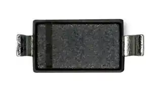


NRVB0530T1G
Schottky Rectifier, 30 V, 500 mA, Single, SOD-123, 2 Pins, 430 mV
- Manufacturer: ONSEMI
- Product type: Schottky Rectifier Diodes
- Repetitive Reverse Voltage Vrrm Max:30V; Forward Current If(AV):500mA; Diode Configuration:Single; Diode Case Style:SOD-123; No. of Pins:2Pins; Forward Voltage VF Max:430mV; Forward
- SVHC: No SVHC (25-Jun-2025)
- No. of Pins: 2Pins
- Product Range: -
- Qualification: AEC-Q101
- Diode Mounting: Surface Mount
- Diode Case Style: SOD-123
- Diode Configuration: Single
- Forward Voltage Max: 430mV
- Forward Surge Current: 5.5A
- Average Forward Current: 500mA
- Operating Temperature Max: 125°C
- Repetitive Peak Reverse Voltage: 30V
| Delivery and price | |
|---|---|
| Units per pack | 1000 |
| Price | 0.084 € |
| Current stock | 1000+ |
| Lead time | 30 days |
MBR0530, NRVB0530 ## Surface Mount Schottky Power Rectifier **Plastic SOD−123 Package** The MBR0530 uses the Schottky Barrier principle with a large area metal−to−silicon power diode. Ideally suited for low voltage, high frequency rectification or as free wheeling and polarity protection diodes in surface mount applications where compact size and weight are critical to the system. This package also provides an easy to work with alternative to leadless 34 package style. These state−of−the−art devices have the following features: ## **http://onsemi.com** **SCHOTTKY BARRIER RECTIFIER 0.5 AMPERES 30 VOLTS** ## **Features** - Guardring for Stress Protection - Low Forward Voltage - 125°C Operating Junction Temperature - Epoxy Meets UL 94, V−0 @ 0.125 in - Package Designed for Optimal Automated Board Assembly - NRVB Prefix for Automotive and Other Applications Requiring Unique Site and Control Change Requirements; AEC−Q101 Qualified and PPAP Capable - These Devices are Pb−Free and are RoHS Compliant* ## **Mechanical Characteristics** - Polarity Designator: Cathode Band - Weight: 11.7 mg (approximately) - Case: Epoxy, Molded - Finish: All External Surfaces Corrosion Resistant and Terminal Leads are Readily Solderable - Lead and Mounting Surface Temperature for Soldering Purposes: 260°C Max. for 10 Seconds **==> picture [38 x 27] intentionally omitted <==** **----- Start of picture text -----**<br> SOD−123<br>CASE 425<br>STYLE 1<br>**----- End of picture text -----**<br> ## **MARKING DIAGRAM** **==> picture [103 x 67] intentionally omitted <==** **----- Start of picture text -----**<br> B3 M<br>1<br>B3 = Device Code<br>M = Date Code<br>= Pb−Free Package<br>**----- End of picture text -----**<br> (Note: Microdot may be in either location) ## **ORDERING INFORMATION** |**Device**|**Package**|**Shipping**†| |---|---|---| |MBR0530T1G|SOD−123<br>(Pb−Free)|3,000 /<br>Tape & Reel **| |NRVB0530T1G|SOD−123<br>(Pb−Free)|3,000 /<br>Tape & Reel **| |MBR0530T3G|SOD−123<br>(Pb−Free)|10.000 /<br>Tape & Reel ***| |NRVB0530T3G|SOD−123<br>(Pb−Free)|10.000 /<br>Tape & Reel ***| - ** 8 mm Tape, 7” Reel - *** 8 mm Tape, 13” Reel - *For additional information on our Pb−Free strategy and soldering details, please download the ON Semiconductor Soldering and Mounting Techniques Reference Manual, SOLDERRM/D. - †For information on tape and reel specifications, including part orientation and tape sizes, please refer to our Tape and Reel Packaging Specifications Brochure, BRD8011/D. Publication Order Number: **MBR0530T1/D** **1** © Semiconductor Components Industries, LLC, 2014 **December, 2014 − Rev. 8** **MBR0530, NRVB0530** ## **MAXIMUM RATINGS** |**MAXIMUM RATINGS**|||| |---|---|---|---| |**Rating**|**Symbol**|**Value**|**Unit**| |Peak Repetitive Reverse Voltage<br>Working Peak Reverse Voltage<br>DC Blocking Voltage|VRRM<br>VRWM<br>VR|30|V| |Average Rectified Forward Current<br>(Rated VR, TL= 100°C)|IF(AV)|0.5|A| |Non−Repetitive Peak Surge Current<br>(Surge Applied at Rated Load Conditions Halfwave, Single Phase, 60 Hz)|IFSM|5.5|A| |Storage Temperature Range|Tstg|−65 to +150|°C| |Operating Junction Temperature|TJ|−65 to +125|°C| |Voltage Rate of Change (Rated VR)|dv/dt|1000|V/�s| |ESD Rating:<br>Machine Model = C<br>Human Body Model = 3B||> 400<br>> 8000|V| Stresses exceeding those listed in the Maximum Ratings table may damage the device. If any of these limits are exceeded, device functionality should not be assumed, damage may occur and reliability may be affected. ## **THERMAL CHARACTERISTICS** |**THERMAL CHARACTERISTICS**|||| |---|---|---|---| |**Characteristic**|**Symbol**|**Value**|**Unit**| |Thermal Resistance − Junction−to−Ambient (Note 1)|R�JA|206|°C/W| |Thermal Resistance − Junction−to−Lead|R�JL|150|°C/W| 1. 1 inch square pad size (1 x 0.5 inch for each lead) on FR4 board. ## **ELECTRICAL CHARACTERISTICS** |**ELECTRICAL CHARACTERISTICS**|||| |---|---|---|---| |**Characteristic**|**Symbol**|**Value**|**Unit**| |Maximum Instantaneous Forward Voltage (Note 2)<br>(iF= 0.1 Amps, TJ= 25°C)<br>(iF= 0.5 Amps, TJ= 25°C)|vF|0.375<br>0.43|V| |Maximum Instantaneous Reverse Current (Note 2)<br>(Rated DC Voltage, TC= 25°C)<br>(VR= 15 V, TC= 25°C)|IR|130<br>20|�A| Product parametric performance is indicated in the Electrical Characteristics for the listed test conditions, unless otherwise noted. Product performance may not be indicated by the Electrical Characteristics if operated under different conditions. 2. Pulse Test: Pulse Width = 300 � s, Duty Cycle ≤ 2%. **==> picture [491 x 171] intentionally omitted <==** **----- Start of picture text -----**<br> 10 [4]<br>1 1000 TJ = 125°C<br>TJ = 125°C 75°C 25°C -�40°C 100 75°C<br>0.1<br>10<br>25°C<br>1<br>0.010.15 0.2 0.25 0.3 0.35 0.4 0.45 0.5 0.55 0 5 10 15 20 25 30 35 40<br>vF, INSTANTANEOUS VOLTAGE (VOLTS) VR, REVERSE VOLTAGE (VOLTS)<br>μ<br>IR, REVERSE CURRENT (��A)<br>iF, INSTANTANEOUS FORWARD CURRENT (AMPS)<br>**----- End of picture text -----**<br> **Figure 1. Typical Forward Voltage** **Figure 2. Typical Reverse Current** **http://onsemi.com** **2** **MBR0530, NRVB0530** **==> picture [243 x 606] intentionally omitted <==** **----- Start of picture text -----**<br> 180<br>160 TYPICAL CAPACITANCE AT 0 V = 170 pF<br>140<br>120<br>100<br>80<br>60<br>40<br>20<br>0 5 10 15 20 25 30<br>VR, REVERSE VOLTAGE (VOLTS)<br>Figure 3. Typical Capacitance<br>1<br>0.875<br>DC<br>0.75<br>0.625 SQUARE WAVE<br>0.5<br>= �<br>0.375<br>= 5<br>0.25 = 10<br>0.125 Ipk/Iav = 20<br>0<br>60 67 74 81 88 95 102 109 116 123 130<br>LEAD TEMPERATURE (°C)<br>Figure 4. Current Derating (Lead)<br>0.35<br>0.315 TJ = 125°C<br>SQUARE WAVE<br>0.28 DC<br>= �<br>0.245<br>= 10 = 5<br>0.21<br>0.175 Ipk/Iav = 20<br>0.14<br>0.105<br>0.07<br>0.035<br>0<br>0 0.1 0.2 0.3 0.4 0.5 0.6 0.7 0.8<br>IF(AV), AVERAGE FORWARD CURRENT (AMP)<br>C, CAPACITANCE (pF)<br>AVERAGE FORWARD CURRENT (AMP)<br>PF(AV), AVERAGE POWER DISSIPATION (WATT)<br>**----- End of picture text -----**<br> **Figure 5. Power Dissipation** **http://onsemi.com** **3** **MBR0530, NRVB0530** ## **PACKAGE DIMENSIONS** **SOD−123** CASE 425−04 ISSUE G **==> picture [429 x 334] intentionally omitted <==** **----- Start of picture text -----**<br> D<br>A NOTES:<br>1. DIMENSIONING AND TOLERANCING PER ANSI<br>A1 Y14.5M, 1982.<br>2. CONTROLLING DIMENSION: INCH.<br>1<br>MILLIMETERS INCHES<br> DIM MIN NOM MAX MIN NOM MAX<br>A 0.94 1.17 1.35 0.037 0.046 0.053<br> A1 0.00 0.05 0.10 0.000 0.002 0.004<br>b 0.51 0.61 0.71 0.020 0.024 0.028<br>HE E c --- --- 0.15 --- --- 0.006<br>D 1.40 1.60 1.80 0.055 0.063 0.071<br>E 2.54 2.69 2.84 0.100 0.106 0.112<br>HE 3.56 3.68 3.86 0.140 0.145 0.152<br>L 0.25 --- --- 0.010 --- ---<br>0° --- 10° 0° --- 10°<br>2<br>od<br>STYLE 1:<br>PIN 1. CATHODE<br>b L 2. ANODE<br>i ne C = [aeeeee<br>SOLDERING FOOTPRINT*<br>0.91<br>0.036<br>ÉÉ ÉÉ<br>ÉÉ ÉÉ 0.0481.22<br>it<br>ÉÉ ÉÉ<br>2.36<br>0.093<br>4.19<br>a 0.165<br>SCALE 10:1 mm<br>: inches<br>**----- End of picture text -----**<br> *For additional information on our Pb−Free strategy and soldering details, please download the ON Semiconductor Soldering and Mounting Techniques Reference Manual, SOLDERRM/D. **ON Semiconductor** and are registered trademarks of Semiconductor Components Industries, LLC (SCILLC). SCILLC reserves the right to make changes without further notice to any products herein. SCILLC makes no warranty, representation or guarantee regarding the suitability of its products for any particular purpose, nor does SCILLC assume any liability arising out of the application or use of any product or circuit, and specifically disclaims any and all liability, including without limitation special, consequential or incidental damages. “Typical” parameters which may be provided in SCILLC data sheets and/or specifications can and do vary in different applications and actual performance may vary over time. All operating parameters, including “Typicals” must be validated for each customer application by customer’s technical experts. SCILLC does not convey any license under its patent rights nor the rights of others. SCILLC products are not designed, intended, or authorized for use as components in systems intended for surgical implant into the body, or other applications intended to support or sustain life, or for any other application in which the failure of the SCILLC product could create a situation where personal injury or death may occur. Should Buyer purchase or use SCILLC products for any such unintended or unauthorized application, Buyer shall indemnify and hold SCILLC and its officers, employees, subsidiaries, affiliates, and distributors harmless against all claims, costs, damages, and expenses, and reasonable attorney fees arising out of, directly or indirectly, any claim of personal injury or death associated with such unintended or unauthorized use, even if such claim alleges that SCILLC was negligent regarding the design or manufacture of the part. SCILLC is an Equal Opportunity/Affirmative Action Employer. This literature is subject to all applicable copyright laws and is not for resale in any manner. ## **PUBLICATION ORDERING INFORMATION** ## **LITERATURE FULFILLMENT** : Literature Distribution Center for ON Semiconductor P.O. Box 5163, Denver, Colorado 80217 USA **Phone** : 303−675−2175 or 800−344−3860 Toll Free USA/Canada **Fax** : 303−675−2176 or 800−344−3867 Toll Free USA/Canada **Email** : orderlit@onsemi.com **N. American Technical Support** : 800−282−9855 Toll Free USA/Canada **ON Semiconductor Website** : **www.onsemi.com** **Europe, Middle East and Africa Technical Support: Order Literature** : http://www.onsemi.com/orderlit Phone: 421 33 790 2910 **Japan Customer Focus Center** For additional information, please contact your local Phone: 81−3−5817−1050 Sales Representative **http://onsemi.com** **MBR0530T1/D** **4**
Updated at June 4, 2026
onsemi is a premier global supplier of intelligent power and sensing technologies, driving disruptive innovations across the automotive, industrial, and cloud infrastructure markets. Recognized for their commitment to sustainability and reliable supply chains, the company accelerates advancements in vehicle electrification, industrial automation, and 5G networks by solving the industry's most complex design challenges. At the core of their portfolio is an industry-leading selection of discrete semiconductors. This extensive range features thousands of high-performance bipolar transistors, single and dual MOSFETs, and a comprehensive array of diodes, including Zener, Schottky, and fast-recovery rectifiers. Engineered for superior thermal performance and energy efficiency, these foundational components are critical for demanding power conversion, switching, and signal conditioning applications. Beyond essential discretes, onsemi provides a robust suite of advanced power management and circuit protection solutions. Their lineup includes intelligent power modules, single IGBTs, and transient voltage suppression (TVS) diodes designed to safeguard sensitive circuitry. Complimented by integrated passive filters, AC/DC LED driver ICs, and specialized sub-2.4GHz RF transceivers, onsemi equips engineers with the scalable, high-quality technologies needed to build a cleaner, smarter, and more connected world.
About Novapart
Novapart is a B2B electronic component broker specialising in stock shortages and cost reduction. We source hard-to-find parts and identify compliant alternatives across a catalogue of 410,000+ components from 500+ manufacturers.
Learn more →Stock Shortage Specialist
When a component is unavailable, discontinued or has an unacceptable lead time, we tap into our network of vetted European and Asian distributors to source what you need — without compromising on quality or traceability.
Request a quote →Compliant Alternatives
We identify pin-to-pin, electrically equivalent substitutes that meet the same certifications (RoHS, AEC-Q100, REACH) as your original specification — validated against datasheets, not just part numbers. Often at a lower cost.
BOM Analysis service →