


NMLU1210TWG
Bridge Rectifier, Single Phase, 20 V, UDFN, 8 Pins, 410 mV
- Manufacturer: ONSEMI
- Product type: Bridge Rectifier Diodes
- No. of Phases:Single Phase; Repetitive Reverse Voltage Vrrm Max:20V; Forward Current If(AV):-; Bridge Rectifier Case Style:UDFN; Forward Voltage VF Max:410mV; No. of Pins:8Pins; Opera
- SVHC: No SVHC (15-Jan-2018)
- No. of Pins: 8Pins
- No. of Phases: Single Phase
- Product Range: -
- Forward Voltage Max: 410mV
- Forward Surge Current: -
- Average Forward Current: -
- Bridge Rectifier Mounting: Surface Mount
- Operating Temperature Max: 125°C
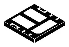
- Bridge Rectifier Case Style: UDFN
- Repetitive Peak Reverse Voltage: 20V
| Delivery and price | |
|---|---|
| Units per pack | 1 |
| Price | 0.406 € |
| Current stock | 10+ |
| Lead time | 30 days |
## NMLU1210

## Full Bridge Rectifier

Dual 20 V N−Channel with dual 3.2 A Schottky Barrier Diode, 4.0 x 4.0 x 0.5 mm Cool nM ™ Package

## **Features**

- Full−Bridge Rectifier Block

- Up to 3.2 A operation

- Low RDS(on) MOSFET to minimize conduction loss

- Low gate charge MOSFET

- Low VF Schottky diode

- Ultra Low Inductance Package

- This Device uses Halogen−Free Molding Compound

- These are Pb−Free Devices

## **Applications**

## **http://onsemi.com**

**==> picture [168 x 97] intentionally omitted <==**

**----- Start of picture text -----**<br>
||||
|---|---|---|
|MOSFET|
|V(BR)DSS|RDS(on) TYP|ID MAX|
|23 m|@ 4.5 V|
|20 V|3.2 A|
|17 m|@ 10 V|
|SCHOTTKY DIODE|
|VR MAX|VF TYP|IF MAX|
|20 V|0.45 V|3.2 A|

**----- End of picture text -----**<br>


- Wireless Charging

- AC−DC Rectification

- Optimized for Power Management Applications for Portable Products, such as Cell Phones, PMP, DSC, GPS, and others

## **RECTIFIER MAXIMUM RATINGS** (TJ = 25 ° C unless otherwise stated)

**==> picture [478 x 246] intentionally omitted <==**

**----- Start of picture text -----**<br>
||||||||||||||
|---|---|---|---|---|---|---|---|---|---|---|---|---|
|Parameter|Symbol|Value|Unit|
|oO|GND1|GND?|
|Input voltage between two MOSFET drain|VLL|20|V|
|RECTIFIER|
|Bridge Operating Junction and Storage|TJ, TSTG|−55 to|°|C|4.0 4.0 mm Cool Pin Connections|
|Temperature|125|(Top View)|
|Lead Temperature for Soldering Purposes|TL|260|°|C|MARKING DIAGRAM|
|(1/8” from case for 10 s)|
|Continuous Drain Current|TA = 25|°C|IO|2.2|A|UDFN|1210|
|R|_|JA (Note 1)|TA = 85|°C|1.16|Ç|CASE 517BS|AYWW|
|Power Dissipation R|_|JA (Note 1)|TTAA = 25 = 85|°°CC|PD|0.471.2|W|ÇÇ1210A|= Specific Device Code= Assembly Location|
|Continuous Drain Current|TA = 25|°C|IO|3.2|A|Y|= Year|
|R|_|JA t < 5 s (Note 1)|TA = 85|°C|1.88|WW|= Work Week= Pb−Free Package|
|Power Dissipation|TA = 25|°C|PD|2.34|W|(*Note: Microdot may be in either location)|
|R|_|JA t < 5 s (Note 1)|TA = 85|°C|0.94|PIN CONNECTIONS|
|Continuous Drain Current|TA = 25|°C|IO|1.16|A|Vout|Vout|Vout|
|R|_|JA (Note 2)|TA = 85|°C|0.6|L1_1|L|S|tet|i|d|L1_2|
|Power Dissipation|TA = 25|°C|PD|0.47|W|GND1GND1GND1|=a|ot|=|GND2GND2GND2|
|R|_|JA (Note 2)|TA = 85|°C|0.185|

**----- End of picture text -----**<br>


**==> picture [86 x 51] intentionally omitted <==**

**----- Start of picture text -----**<br>
Vout Vout Vout<br>L1_1 L S tet i d L1_2<br>GND1GND1GND1 =a ot = GND2GND2GND2<br>(Top View)<br>L1_1 L1_2<br>**----- End of picture text -----**<br>


Stresses exceeding Maximum Ratings may damage the device. Maximum Ratings are stress ratings only. Functional operation above the Recommended Operating Conditions is not implied. Extended exposure to stresses above the Recommended Operating Conditions may affect device reliability.

## **ORDERING INFORMATION**

**==> picture [185 x 35] intentionally omitted <==**

**----- Start of picture text -----**<br>
|||||
|---|---|---|---|
|Device|Package|Shipping|[†]|
|UDFN|
|NMLU1210TWG|3000 / Tape & Reel|
|(Pb−Free)|

**----- End of picture text -----**<br>


1. Surface−mounted on FR4 board using 1 in sq pad size (Cu area = 1.127 in sq [2 oz] including traces).

2. Surface−mounted on FR4 board using the minimum recommended pad size of 30 mm[2] , 2 oz. Cu.

- †For information on tape and reel specifications, including part orientation and tape sizes, please refer to our Tape and Reel Packaging Specifications Brochure, BRD8011/D.

Publication Order Number: **NMLU1210/D**

**1**

© Semiconductor Components Industries, LLC, 2013 **August, 2013 − Rev. 1**

**NMLU1210**

## **THERMAL RESISTANCE RATINGS**

|**THERMAL RESISTANCE RATINGS**||||
|---|---|---|---|
|**Parameter**|**Symbol**|**Max**|**Unit**|
|Junction−to−Ambient – Steady State (Note 3)|RθJA|82.5|°C/W|
|Junction−to−Ambient – t≤5 s (Note 3)|RθJA|42.5||
|Junction−to−Ambient – Steady State min Pad (Note 4)|RθJA|209||


3. Surface−mounted on FR4 board using 1 in sq pad size (Cu area = 1.127 in sq [2 oz] including traces).

4. Surface−mounted on FR4 board using the minimum recommended pad size of 30 mm[2] , 2 oz. Cu.

**BRIDGE ELECTRICAL CHARACTERISTICS** (TJ = 25 ° C unless otherwise specified)

|**Parameter**|**Symbol**|**Test Condition**|**Min**|**Typ**|**Max**|**Unit**|
|---|---|---|---|---|---|---|
|**ON CHARACTERISTICS**|||||||
|Rectifying Forward Voltage (Note 5)|Vfd2|Input voltage VLL=±5 V;<br>The output current of Rectifier Iout= 2 A||0.45|.56|V|
|Rectifier leakage current|Ileak|Input voltage VLL= 16 V;<br>No Load on the Rectifier output||31|1000|uA|
|Rectifier Reverse leakage current|Irleak|Input voltage VLL= 0 V;<br>The output voltage of the Rectifier<br>Vout= 5 V||21|1000|uA|


5. Pulse Test: pulse width ≤ 300 � s, duty cycle ≤ 2%

**MOSFET ELECTRICAL CHARACTERISTICS** (TJ = 25 ° C unless otherwise specified)

|**Parameter**|**Symbol**|**Test Condition**|**Test Condition**|**Min**|**Typ**|**Max**|**Unit**|
|---|---|---|---|---|---|---|---|
|**ON CHARACTERISTICS**||||||||
|Gate Threshold Voltage|VGS(TH)|VGS= VDS, ID=|250�A|1.2||2.2|V|
|Negative Threshold Temperature<br>Coefficient|VGS(TH)/<br>TJ||||4||mV/°C|
|Drain−to−Source On Resistance<br>(Note 6)|RDS(on)|VGS= 10 V, ID=|3.2 A||17|26|m�|
|||VGS= 4.5 V, ID|= 3.2 A||23|32||
|Forward Transconductance|gFS|VDS = 10 V, ID|= 2.0 A||3.5||S|
|**DRAIN−SOURCE DIODE CHARACTERISTICS**||||||||
|Forward Diode Voltage (Note 6)|VSD|VGS= 0 V, IS= 2.0 A|TJ= 25°C||0.79||V|
||||TJ= 125°C||0.65|||


6. Pulse Test: pulse width ≤ 300 � s, duty cycle ≤ 2%

## **SCHOTTKY DIODE ELECTRICAL CHARACTERISTICS** (TJ = 25 ° C unless otherwise specified)

|**SCHOTTKY DIODE ELECTRICAL**|**CHARACT**|**ERISTICS**(TJ= 25°C unless otherwise sp|ecified)||||
|---|---|---|---|---|---|---|
|**Parameter**|**Symbol**|**Test Condition**|**Min**|**Typ**|**Max**|**Unit**|
|Maximum Instantaneous Forward<br>Voltage (Note 7)|VF|IF= 1.0 A||0.36||V|
|||IF= 2.0 A||0.41|||
|Maximum Instantaneous Reverse<br>Current|IR|VR=  20 V||0.04||mA|


7. Pulse Test: pulse width ≤ 300 � s, duty cycle ≤ 2%

## **SCHOTTKY DIODE ELECTRICAL CHARACTERISTICS** (TJ = 100 ° C unless otherwise specified)

|**SCHOTTKY DIODE ELECTRICAL**|**CHARACT**|**ERISTICS**(TJ= 100°C unless otherwise s|pecified)||||
|---|---|---|---|---|---|---|
|**Parameter**|**Symbol**|**Test Condition**|**Min**|**Typ**|**Max**|**Unit**|
|Maximum Instantaneous Forward<br>Voltage (Note 8)|VF|IF= 1.0 A||0.29||V|
|||IF= 2.0 A||0.36|||
|Maximum Instantaneous Reverse<br>Current|IR|VR=  20 V||4||mA|


8. Pulse Test: pulse width ≤ 300 � s, duty cycle ≤ 2%

9. For detailed MOSFET and Diode parameters, please refer to the ON Semiconductor datasheets of NTTFS4930N and MBR230LSFT1G. The test on each individual die is limited to the system package.

**http://onsemi.com**

**2**

**NMLU1210**

**Figure 1. Typical Application Circuit**

GND1 and GND2 are not internally connected. The user should make the connection in the PCB design.

**http://onsemi.com 3**

**NMLU1210**

## **TYPICAL PERFORMANCE CURVES**

(TJ = 25 ° C unless otherwise specified)

**==> picture [490 x 605] intentionally omitted <==**

**----- Start of picture text -----**<br>
10 10<br>−55 ° C<br>125 ° C 25 ° C<br>1 125 ° C 1<br>25 ° C<br>−55 ° C<br>0.1 0.1<br>0 0.2 0.4 0.6 0.8 1.0 1.2 1.4 1.6 1.8 0 0.2 0.4 0.6 0.8 1.0 1.2 1.4 1.6 1.8<br>VF, INSTANTANEOUS FORWARD VOLTAGE (V) VF, INSTANTANEOUS FORWARD VOLTAGE (V)<br>Figure 2. Bridge Typical Forward Voltage Drop Figure 3. Bridge Maximum Forward Voltage<br>at Vin �  5 V Drop at Vin �  5 V<br>10k 1k<br>1k<br>100<br>Maximum<br>100 Maximum<br>10<br>10<br>Typical<br>1<br>1 Typical<br>0.1<br>0.1<br>0.01 0.01<br>25 35 45 55 65 75 85 95 105 115 125 25 35 45 55 65 75 85 95 105 115 125<br>TJ, TEMPERATURE JUNCTION ( ° C) TJ, TEMPERATURE JUNCTION ( ° C)<br>Figure 4. Output Leakage at 5 V Bias vs. Figure 5. Input Leakage at 16 V vs. Junction<br>Junction Temperature Temperature<br>700 40<br>600 T IDJ = 2 A  = 25 ° C TIJD = 25 = 2 A ° C<br>35<br>500<br>400 30<br>300<br>25<br>200<br>20<br>100<br>0 15<br>2.0 3.0 4.0 5.0 6.0 7.0 8.0 9.0 10<br>2.0 3.0 4.0 5.0 6.0 7.0 8.0 9.0 10<br>VGS (V)<br>VGS, GATE−TO−SOURCE VOLTAGE (V)<br>CURRENT (A) CURRENT (A)<br>, INSTANTANEOUS FORWARD , INSTANTANEOUS FORWARD<br>IF IF<br>, OUTPUT LEAKAGE (mA)<br>OUTPUT LEAKAGE (mA)<br>ILEAK<br>) � ) �<br> (m  (m<br>DS(on) DS(on)<br>R R<br>**----- End of picture text -----**<br>


**Figure 6. FET Typical On−Resistance vs. Gate−to−Source Voltage ( from 3 V to 10 V)**

**Figure 7. FET Typical On−Resistance vs. Gate−to−Source Voltage**

**http://onsemi.com**

**4**

**NMLU1210**

## **TYPICAL PERFORMANCE CURVES**

(TJ = 25 ° C unless otherwise specified)

**==> picture [490 x 197] intentionally omitted <==**

**----- Start of picture text -----**<br>
10 100<br>125 ° C<br>10<br>1.0<br>1 125 ° C<br>0.1<br>25 ° C<br>25 ° C<br>−55 ° C 0.01<br>0.1 0.001<br>0 0.1 0.2 0.3 0.4 0.5 0.6 0.7 0.8 0.9 0 5 10 15 20 25<br>VF, INSTANTANEOUS FORWARD VOLTAGE (V) VR, INSTANTANEOUS REVERSE VOLTAGE (V)<br>Figure 8. Schottky Typical Forward Current vs. Figure 9. Schottky Typical Reverse Current vs.<br>Forward Voltage Reverse Voltage<br>CURRENT (A)<br>CURRENT (mA)<br>, INSTANTANEOUS FORWARDIF , INSTANTANEOUS REVERSEIR<br>**----- End of picture text -----**<br>


**http://onsemi.com**

**5**

**NMLU1210**

## **PACKAGE DIMENSIONS**

**==> picture [470 x 440] intentionally omitted <==**

**----- Start of picture text -----**<br>
UDFN8 4x4, 0.8P<br>CASE 517BS<br>ISSUE A<br>D A L NOTES:<br>1. DIMENSIONING AND TOLERANCING PER<br>B L3 L3 ASME Y14.5M, 1994.<br>2. CONTROLLING DIMENSION: MILLIMETERS.<br>3. DIMENSION b APPLIES TO PLATED<br>TERMINAL AND IS MEASURED BETWEEN<br>REFERENCEPIN ONE ÉÉÉ mae, E L “oto DETAIL AL1 art oe 4. 0.15 AND 0.25MM FROM TERMINAL TIP.COPLANARITY APPLIES TO THE EXPOSEDPAD AS WELL AS THE TERMINALS.<br>a c 0.15 ot C ÉÉÉ ! |p CONSTRUCTIONSALTERNATE 5. POSITIONAL TOLERANCE APPLIES TO ALLOF THE EXPOSED PADS.<br>MILLIMETERS<br>0.15 C DIM MIN MAX<br>e lo TOP VIEW EXPOSED Cu MOLD CMPD - A3 A1A 0.450.00 0.550.05<br>A3 0.13 REF<br>DETAIL B A ÇÇÉÉ ÉÉÇÇ b 0.20 0.30<br>0.10 C D 4.00 BSC<br>0.08 C ÇÇÇÇ (A3) ÇÇ ÉÉ DETAIL B A1 ÇÇ D3D2E 0.902.104.00 BSC1.102.30<br>NOTE 4 SIDE VIEW A1 C SEATINGPLANE CONSTRUCTIONSALTERNATE E3E2 1.002.50 1.202.70<br>e 0.80 BSC<br>F 3.55 BSC<br>D3 e 0.10 on M C A B L1L 0.300.00 0.500.15<br>D2 NOTE 5 L3 0.13 0.23<br>DETAIL A F/2 RECOMMENDED<br>1 4 2X E3 0.10 M C A B SOLDERING FOOTPRINT*<br>4X<br>E2 NOTE 5 0.35 6X<br>2.34 0.60<br>fad ao +r<br>8 5 PACKAGE<br>8X b OUTLINE<br>e 0.10 M C A B 4.15 2.74<br>e/2<br>0.05 M C NOTE 3<br>& F | Seb<br>0.80 2X<br>BOTTOM VIEW 0.40 1 1.24<br>1.14 DETAIL C<br>3.69<br>2X 1.15<br>0.80 DIMENSIONS: MILLIMETERS<br>DETAIL C<br>*For additional information on our Pb−Free strategy and soldering<br>details, please download the ON Semiconductor Soldering and<br>Mounting Techniques Reference Manual, SOLDERRM/D.<br>**----- End of picture text -----**<br>


Cool is a trademark of Semiconductor Components Industries, LLC (SCILLC).

**ON Semiconductor** and          are registered trademarks of Semiconductor Components Industries, LLC (SCILLC).  SCILLC owns the rights to a number of patents, trademarks, copyrights, trade secrets, and other intellectual property. A listing of SCILLC’s product/patent coverage may be accessed at www.onsemi.com/site/pdf/Patent−Marking.pdf.  SCILLC reserves the right to make changes without further notice to any products herein.  SCILLC makes no warranty, representation or guarantee regarding the suitability of its products for any particular purpose, nor does SCILLC assume any liability arising out of the application or use of any product or circuit, and specifically disclaims any and all liability, including without limitation special, consequential or incidental damages.  “Typical” parameters which may be provided in SCILLC data sheets and/or specifications can and do vary in different applications and actual performance may vary over time.  All operating parameters, including “Typicals” must be validated for each customer application by customer’s technical experts.  SCILLC does not convey any license under its patent rights nor the rights of others.  SCILLC products are not designed, intended, or authorized for use as components in systems intended for surgical implant into the body, or other applications intended to support or sustain life, or for any other application in which the failure of the SCILLC product could create a situation where personal injury or death may occur.  Should Buyer purchase or use SCILLC products for any such unintended or unauthorized application, Buyer shall indemnify and hold SCILLC and its officers, employees, subsidiaries, affiliates, and distributors harmless against all claims, costs, damages, and expenses, and reasonable attorney fees arising out of, directly or indirectly, any claim of personal injury or death associated with such unintended or unauthorized use, even if such claim alleges that SCILLC was negligent regarding the design or manufacture of the part.  SCILLC is an Equal Opportunity/Affirmative Action Employer.  This literature is subject to all applicable copyright laws and is not for resale in any manner.

## **PUBLICATION ORDERING INFORMATION**

**LITERATURE FULFILLMENT** : **N. American Technical Support** : 800−282−9855 Toll Free **ON Semiconductor Website** : **www.onsemi.com** Literature Distribution Center for ON Semiconductor USA/Canada P.O. Box 5163, Denver, Colorado 80217 USA **Europe, Middle East and Africa Technical Support: Order Literature** : http://www.onsemi.com/orderlit **Phone** : 303−675−2175 or 800−344−3860 Toll Free USA/Canada Phone: 421 33 790 2910 **Fax** : 303−675−2176 or 800−344−3867 Toll Free USA/Canada **Japan Customer Focus Center** For additional information, please contact your local **Email** : orderlit@onsemi.com Phone: 81−3−5817−1050 Sales Representative

## **LITERATURE FULFILLMENT** :

**NMLU1210/D**

**http://onsemi.com 6**
Updated at June 4, 2026
onsemi is a premier global supplier of intelligent power and sensing technologies, driving disruptive innovations across the automotive, industrial, and cloud infrastructure markets. Recognized for their commitment to sustainability and reliable supply chains, the company accelerates advancements in vehicle electrification, industrial automation, and 5G networks by solving the industry's most complex design challenges. At the core of their portfolio is an industry-leading selection of discrete semiconductors. This extensive range features thousands of high-performance bipolar transistors, single and dual MOSFETs, and a comprehensive array of diodes, including Zener, Schottky, and fast-recovery rectifiers. Engineered for superior thermal performance and energy efficiency, these foundational components are critical for demanding power conversion, switching, and signal conditioning applications. Beyond essential discretes, onsemi provides a robust suite of advanced power management and circuit protection solutions. Their lineup includes intelligent power modules, single IGBTs, and transient voltage suppression (TVS) diodes designed to safeguard sensitive circuitry. Complimented by integrated passive filters, AC/DC LED driver ICs, and specialized sub-2.4GHz RF transceivers, onsemi equips engineers with the scalable, high-quality technologies needed to build a cleaner, smarter, and more connected world.
About Novapart
Novapart is a B2B electronic component broker specialising in stock shortages and cost reduction. We source hard-to-find parts and identify compliant alternatives across a catalogue of 420,000+ components from 500+ manufacturers.
Learn more →Stock Shortage Specialist
When a component is unavailable, discontinued or has an unacceptable lead time, we tap into our network of vetted European and Asian distributors to source what you need — without compromising on quality or traceability.
Request a quote →Compliant Alternatives
We identify pin-to-pin, electrically equivalent substitutes that meet the same certifications (RoHS, AEC-Q100, REACH) as your original specification — validated against datasheets, not just part numbers. Often at a lower cost.
BOM Analysis service →