
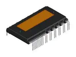


NFAM2065L4BT
Intelligent Power Module (IPM), IGBT, 650 V, 20 A, 2.5 kV, DIP, SPM31
- Manufacturer: ONSEMI
- Product type: Intelligent Power Modules
- SVHC: No SVHC (25-Jun-2025)
- IPM Series: SPM31
- Product Range: SPM31 Series
- IPM Case Style: DIP
- IPM Power Device: IGBT
- Isolation Voltage: 2.5kV
- Current Rating (Ic / Id): 20A
- Voltage Rating (Vces / Vdss): 650V
| Delivery and price | |
|---|---|
| Units per pack | 50 |
| Price | 12.82 € |
| Current stock | 50+ |
| Lead time | 30 days |
## Intelligent Power Module (IPM) 650 V, 20 A

## NFAM2065L4BT

## **General Description**

The NFAM2065L4BT is a fully−integrated inverter power module consisting of an independent High side gate driver, LVIC, six IGBT’s and a temperature sensor (VTS or Thermistor(T)), suitable for driving permanent magnet synchronous (PMSM) motors, brushless DC (BLDC) motors and AC asynchronous motors. The IGBT’s are configured in a three−phase bridge with separate emitter connections for the lower legs for maximum flexibility in the choice of control algorithm.

**www.onsemi.com**

The power stage has under−voltage lockout protection (UVP). Internal boost diodes are provided for high side gate boost drive.

## **Features**

- Three−phase 650 V, 20 A IGBT Module with Independent Drivers

- Active Logic Interface

**DIP39 54.5 x 31.0 CASE MODGC**

- Built−in Under−voltage Protection (UVP)

- Integrated Bootstrap Diodes and Resistors

## **MARKING DIAGRAM**

- Separate Low−side IGBT Emitter Connections for Individual Current Sensing of Each Phase

- Temperature Sensor (VTS or Thermistor (T))

- UL1557 Certified (File No.E339285)

- This is a Pb−Free Device

NFAM2065L4BT ZZZATYWW

## **Typical Application**

- Industrial Drives

- Industrial Pumps

- Industrial Fans

- Industrial Automation

**==> picture [230 x 143] intentionally omitted <==**

**----- Start of picture text -----**<br>
RTH VTH P U V W<br>VS(U)<br>VDD(UH)VB(U) High SideHVIC1 HS1<br>HIN(U)<br>VS(V)<br>VDD(VH)VB(V) High SideHVIC2 HS2 HS1 HS2 HS3<br>HIN(V)<br>VS(W)<br>VDD(WH)VB(W) Pe= High SideHVIC3 HS3 aRARR<br>HIN(W)<br>VTS LS1 LS2 LS3<br>LIN(U)<br>LIN(V) Low Side LS1<br>LIN(W)CFODVFOCIN ProtectionLVICwith LS2LS3<br>VSS<br>VDD(L)<br>NU NV NW<br>**----- End of picture text -----**<br>


Device marking is on package top side

NFAM2065L4BT = Specific Device Code ZZZ = Assembly Lot Code A = Assembly Location T = Test Location Y = Year WW = Work Week

## **ORDERING INFORMATION**

|**Device**|**Package**|**Shipping**<br>**(Qty / Packing)**|
|---|---|---|
|NFAM2065L4BT|DIP39, 31.0x54.5<br>(Pb−Free)|90 / BOX|


**Figure 1. Application Schematic**

Publication Order Number: **NFAM2065L4BT/D**

**1**

© Semiconductor Components Industries, LLC, 2019 **April, 2020 − Rev. 1**

**NFAM2065L4BT**

## **APPLICATION SCHEMATIC**

**==> picture [472 x 464] intentionally omitted <==**

**----- Start of picture text -----**<br>
5 V line<br>RTH (39)<br>VB(U) (3) VTH (38)<br>VS(U) (1) P (37)<br>CS + C1<br>HIN (U) (6) HIN HOUTVB<br>VDD(UH) (4) VDD HVIC 1<br>VSS VS U (36)<br>VB(V) (9)<br>VS(V) (7)<br>HIN (V) (12) VB<br>HIN HOUT<br>VDD(VH) (10) HVIC 2<br>VDD<br>VSS VS V (35) Motor<br>VB(W) (15)<br>VS(W) (13)<br>MCU HIN (W) (18) VB<br>HIN HOUT<br>VDD(WH) (16) HVIC 3<br>VDD<br>VSS VS W (34)<br>VTS (20) VTS<br>LIN(U) (21) OUT(U)<br>LIN(U)<br>LIN(V) (22) LIN(V) NU (33)<br>LIN(W) (23)<br>LIN(W)<br>5 V line<br>LVIC<br>VFO (24) VFO OUT(V)<br>CFOD (25)<br>CFOD NV (32)<br>15 V lineCIN (26) CIN<br>VDD(L) (28)<br>VDD<br>VSS (27) VSS OUT(W)<br>NW (31)<br>Signal for short circuit trip<br>Phase current<br>**----- End of picture text -----**<br>


**Figure 2. Application Schematic − Adjustable Option**

**www.onsemi.com**

**2**

**NFAM2065L4BT**

## **BLOCK DIAGRAM**

**==> picture [499 x 446] intentionally omitted <==**

**----- Start of picture text -----**<br>
RTH (39<br>* NTC Thermistor<br>VTH (38)<br>VS(U) (1)<br>P (37)<br>VB (U) (3)<br>VB<br>VDD (UH ) (4) VDD HOUT<br>HVIC 1<br>HIN (U) (6) HIN<br>VSS V S U (36)<br>VS(V) (7)<br>VB(V)(9)<br>VB<br>VDD (VH ) (10 ) VDD HOUT<br>HVIC 2<br>HIN (V) (12 ) HIN<br>VSS VS V (35 )<br>VS(W) (13 )<br>VB(W) (15 )<br>VB<br>VDD (WH ) (16 ) VDD HOUT<br>HVIC 3<br>HIN (W) (18 ) HIN<br>VSS VS W (34)<br>VTS (20) VTS OUT (U)<br>LIN (U) (21 ) LIN(U)<br>NU (33 )<br>LIN (V) (22 ) LIN(V)<br>LIN (W) (23 ) LIN(W)<br>VFO (24 ) VFO LVIC OUT (V)<br>CFOD (25 ) CFOD<br>NV (32 )<br>CIN (26 ) CIN<br>VSS (27 ) VSS<br>VDD (L) (28 ) VDD OUT (W)<br>NW (31 )<br>**----- End of picture text -----**<br>


**Figure 3. Equivalent Block Diagram**

**www.onsemi.com**

**3**

**NFAM2065L4BT**

## **PIN FUNCTION DESCRIPTION**

|**Pin**|**Name**|**Description**|
|---|---|---|
|1|VS(U)|High−Side Bias Voltage GND for U Phase IGBT Driving|
|(2)|−|Dummy|
|3|VB(U)|High−Side Bias Voltage for U Phase IGBT Driving|
|4|VDD(UH)|High−Side Bias Voltage for U Phase IC|
|(5)|−|Dummy|
|6|HIN(U)|Signal Input for High−Side U Phase|
|7|VS(V)|High−Side Bias Voltage GND for V Phase IGBT Driving|
|(8)|−|Dummy|
|9|VB(V)|High−Side Bias Voltage for V Phase IGBT Driving|
|10|VDD(VH)|High−Side Bias Voltage for V Phase IC|
|(11)|−|Dummy|
|12|HIN(V)|Signal Input for High−Side V Phase|
|13|VS(W)|High−Side Bias Voltage GND for W Phase IGBT Driving|
|(14)|−|Dummy|
|15|VB(W)|High−Side Bias Voltage for W Phase IGBT Driving|
|16|VDD(WH)|High−Side Bias Voltage for W Phase IC|
|(17)|−|Dummy|
|18|HIN(W)|Signal Input for High−Side W Phase|
|(19)|−|Dummy|
|20|VTS|Voltage Output for LVIC Temperature Sensing Unit|
|21|LIN(U)|Signal Input for Low−Side U Phase|
|22|LIN(V)|Signal Input for Low−Side V Phase|
|23|LIN(W)|Signal Input for Low−Side W Phase|
|24|VFO|Fault Output|
|25|CFOD|Capacitor for Fault Output Duration Selection|
|26|CIN|Input for Current Protection|
|27|VSS|Low−Side Common Supply Ground|
|28|VDD(L)|Low−Side Bias Voltage for IC and IGBTs Driving|
|(29)|−|Dummy|
|(30)|−|Dummy|
|31|NW|Negative DC−Link Input for U Phase|
|32|NV|Negative DC−Link Input for V Phase|
|33|NU|Negative DC−Link Input for W Phase|
|34|W|Output for U Phase|
|35|V|Output for V Phase|
|36|U|Output for W Phase|
|37|P|Positive DC−Link Input|
|38|VTH|Thermistor Bias Voltage (T) / Not connection|
|39|RTH|Series Resister for Thermistor (Temperature Detection)  *optional for T|


1. Pins of () are the dummy for internal connection. These pins should be no connection.

**www.onsemi.com**

**4**

## **NFAM2065L4BT**

## **ABSOLUTE MAXIMUM RATINGS** (TC = 25 ° C) (Note 2)

|**Rating**|**Symbol**|**Conditions**|**Value**|**Unit**|
|---|---|---|---|---|
|Supply Voltage|VPN|P − NU, NV, NW|450|V|
|Supply Voltage (Surge)|VPN(Surge)|P − NU, NV, NW, (Note 3)|550|V|
|Self Protection Supply Voltage Limit<br>(Short−Circuit Protection Capability)|VPN(PROT)|VDD = VBS = 13.5 V ~ 16.5 V, Tj = 150°C,<br>Vces < 650 V, Non−Repetitive, < 2 us|400|V|
|Collector−Emitter Voltage|Vces||650|V|
|Maximum Repetitive Revers Voltage|VRRM||650|V|
|Each IGBT Collector Current|±Ic||±20|A|
|Each IGBT Collector Current (Peak)|±Icp|Under 1 ms Pulse Width|±40|A|
|Control Supply Voltage|VDD|VDD(UH,VH,WH), VDD(L) − VSS|−0.3 to 20|V|
|High−Side Control Bias Voltage|VBS|VB(U) − VS(U), VB(V) − VS(V), VB(W) − VS(W)|−0.3 to 20|V|
|Input Signal Voltage|VIN|HIN(U), HIN(V), HIN(W), LIN(U), LIN(V),<br>LIN(W) − VSS|−0.3 to VDD|V|
|Fault Output Supply Voltage|VFO|VFO − VSS|−0.3 to VDD|V|
|Fault Output Current|IFO|Sink Current at VFO pin|2|mA|
|Current Sensing Input Voltage|VCIN|CIN − VSS|−0.3 to VDD|V|
|Corrector Dissipation|Pc|Per One Chip|96|W|
|Operating Junction Temperature|Tj||−40 to +150|°C|
|Storage Temperature|Tstg||−40 to +125|°C|
|Module Case Operation Temperature|Tc||−40 to +125|°C|
|Isolation Voltage|Viso|60 Hz, Sinusoidal, AC 1 minute,<br>Connection Pins to Heat Sink Plate|2500|V rms|


Stresses exceeding those listed in the Maximum Ratings table may damage the device. If any of these limits are exceeded, device functionality should not be assumed, damage may occur and reliability may be affected.

2. Refer to ELECTRICAL CHARACTERISTICS, RECOMMENDED OPERATING RANGES and/or APPLICATION INFORMATION for Safe Operating parameters.

3. This surge voltage developed by the switching operation due to the wiring inductance between P and NU, NV, NW terminal.

## **THERMAL CHARACTERISTICS**

|**Rating**|**Symbol**|**Conditions**|**Min**|**Typ**|**Max**|**Unit**|
|---|---|---|---|---|---|---|
|Junction to Case Thermal<br>Resistance|Rth(j−c)Q|Inverter IGBT Part  (per 1/6 Module)|−|−|1.3|°C/W|
||Rth(j−c)F|Inverter FWDi Part  (per 1/6 Module)|−|−|2.4|°C/W|


4. Refer to ELECTRICAL CHARACTERISTICS, RECOMMENDED OPERATING RANGES and/or APPLICATION INFORMATION for Safe Operating parameters.

**RECOMMENDED OPERATING RANGES** (Note 5)

|**Rating**|**Symbol**|**Conditions**|**Conditions**|**Min**|**Typ**|**Max**|**Unit**|
|---|---|---|---|---|---|---|---|
|Supply Voltage|VPN|P − NU, NV, NW||−|300|400|V|
|Gate Driver Supply Voltages|VDD|VDD(UH,VH,WH), VDD(L) − VSS||13.5|15|16.5|V|
||VBS|VB(U) − VS(U), VB(V) − VS(V),<br>VB(W) − VS(W)||13.0|15|18.5|V|
|Supply Voltage Variation|dVDD / dt<br>dVBS / dt|||−1|−|1|V/�s|
|PWM Frequency|fPWM|||1||20|kHz|
|Dead Time|DT|Turn−off to Turn−on (external)||1.5|−|−|�s|
|Allowable r.m.s. Current|Io|VPN =  300 V,<br>VDD = VD = 15 V,<br>P.F. = 0.8,<br>Tc≤125°C, Tj≤150°C,<br>(Note 5)|fPWM =<br>5 kHz|−|−|20.5|A rms|
||||fPWM =<br>15 kHz|−|−|15.4||


**www.onsemi.com**

**5**

**NFAM2065L4BT**

## **RECOMMENDED OPERATING RANGES** (Note 5) (continued)

|**Rating**|**Symbol**|**Conditions**|**Min**|**Typ**|**Max**|**Unit**|
|---|---|---|---|---|---|---|
|Allowable Input Pulse Width|PWIN (on)|200 V≤VPN≤400 V,<br>13.5 V≤VDD≤16.5 V,<br>13.0 V≤VBS≤18.5 V,<br>−20°C≤Tc≤100°C|1.0<br>1.5|−|−|�s|
||PWIN (off)|||−|−||
|Package Mounting Torque||M3 Type Screw|0.6|0.7|0.9|Nm|


Functional operation above the stresses listed in the Recommended Operating Ranges is not implied. Extended exposure to stresses beyond the Recommended Operating Ranges limits may affect device reliability.

5. Allowable r.m.s Current depends on the actual conditions.

6. Flatness tolerance of the heatsink should be within −50 � m to +100 � m.

**ELECTRICAL CHARACTERISTICS** (Tc = 25 ° C, VDD = 15 V, VBS = 15 V, unless otherwise noted) (Note 7)

|**Parameter**|**Parameter**|**Test Conditions**|**Test Conditions**|**Symbol**|**Min**|**Typ**|**Max**|**Unit**|
|---|---|---|---|---|---|---|---|---|
|**INVERTER SECTION**|||||||||
|Collector−Emitter Leakage<br>Current||Vce = Vces, Tj = 25°C||Ices|−|−|1|mA|
|||Vce = Vces, Tj = 150°C|||−|−|10|mA|
|Collector−Emitter Saturation<br>Voltage||VDD = VBS = 15 V, IN = 5 V<br>Ic = 20 A, Tj = 25°C||VCE(sat)|−|1.60|2.30|V|
|||VDD = VBS = 15 V, IN = 5 V<br>Ic = 20 A, Tj = 150°C|||−|1.80|−|V|
|FWDi Forward Voltage||IN = 0 V, If = 20 A, Tj = 25°C||VF|−|1.90|2.30|V|
|||IN = 0 V, If = 20 A, Tj = 150°C|||−|1.90|−|V|
|High Side|Switching Times|VPN = 300 V, VDD(H) = VDD(L) = 15 V<br>Ic = 20 A, Tj = 25°C, IN = 0⇔5 V<br>Inductive Load||ton|0.80|1.30|1.90|�s|
|||||tc (on)|−|0.20|0.60|�s|
|||||toff|−|1.40|2.00|�s|
|||||tc (off)|−|0.20|0.70|�s|
|||||trr|−|0.15|−|�s|
|Low Side|Switching Times|VPN = 300 V, VDD(H) = VDD(L) = 15 V<br>Ic = 20 A, Tj = 25°C, IN = 0⇔5 V<br>Inductive Load||ton|0.80|1.40|2.00|�s|
|||||tc (on)|−|0.20|0.60|�s|
|||||toff|−|1.50|2.10|�s|
|||||tc (off)|−|0.20|0.70|�s|
|||||trr|−|0.15|−|�s|
|**DRIVER SECTION**|||||||||
|Quiescent VDD Supply Current||VDD(UH,VH,WH) = 15 V,<br>HIN(U,V,W) = 0 V|VDD(UH) − VSS<br>VDD(VH) − VSS<br>VDD(WH) − VSS|IQDDH|−|−|0.30|mA|
|||VDD(L) = 15 V,<br>LIN(U, V, W) = 0 V|VDD(L) − VSS|IQDDL|−|−|3.50|mA|
|Operating VDD Supply Current||VDD(UH, VH, WH) = 15 V,<br>fPWM = 20 kHz, Duty = 50%,<br>Applied to one PWM Signal Input<br>for High−Side|VDD(UH) − VSS<br>VDD(VH) − VSS<br>VDD(WH) − VSS|IPDDH|−|−|0.40|mA|
|||VDD(L) = 15 V,<br>fPWM = 20 kHz, Duty = 50%,<br>Applied to one PWM Signal Input<br>for Low−Side|VDD(L) − VSS|IPDDL|−|−|6.00|mA|
|Quiescent VBS Supply Current||VBS = 15 V<br>HIN(U, V, W) = 0 V|VB(U) − VS(U)<br>VB(V) − VS(V)<br>VB(W) − VS(W)|IQBS|−|−|0.30|mA|


**www.onsemi.com**

**6**

**NFAM2065L4BT**

**ELECTRICAL CHARACTERISTICS** (Tc = 25 ° C, VDD = 15 V, VBS = 15 V, unless otherwise noted) (Note 7) (continued)

|**Parameter**|**Test Conditions**|**Test Conditions**|**Symbol**|**Min**|**Typ**|**Max**|**Unit**|
|---|---|---|---|---|---|---|---|
|**DRIVER SECTION**||||||||
|Operating VBS Supply Current|VDD = VBS = 15 V,<br>fPWM = 20 kHz, Duty = 50%,<br>Applied to one PWM Signal Input<br>for High−Side|VB(U) − VS(U)<br>VB(V) − VS(V)<br>VB(W) − VS(W)|IPBS|−|−|5.00|mA|
|ON Threshold Voltage|HIN(U, V, W) − VSS, LIN(U, V, W) − VSS||VIN(ON)|−|−|2.6|V|
|OFF Threshold Voltage|||VIN(OF)|0.8|−|−|V|
|Short Circuit Trip Level|VDD = 15 V, CIN−VSS||VCIN(ref)|0.46|0.48|0.50|V|
|Supply Circuit Under−Voltage<br>Protection|Detection Level||UVDDD|10.3|−|12.5|V|
||Reset Level||UVDDR|10.8|−|13.0|V|
||Detection Level||UVBSD|10.0|−|12.0|V|
||Reset Level||UVBSR|10.5|−|12.5|V|
|Voltage Output for LVIC<br>Temperature Sensing Unit|VTS−VSS = 10 nF, Temp. = 25°C||VTS|0.905|1.030|1.155|V|
|Fault Output Voltage|VDD = 0 V, CIN = 0 V,<br>VFO Circuit: 10 k�to 5 V Pull−up||VFOH|4.9|−|−|V|
||VDD = 0 V, CIN = 1 V,<br>VFO Circuit: 10 k�to 5 V Pull−up||VFOL|−|−|0.95|V|
|Fault−Output Pulse Width|CFOD = 22 nF||tFOD|1.6|2.4|−|ms|
|**BOOTSTRAP SECTION**||||||||
|Bootstrap Diode Forward Voltage|If = 0.1 A||VF|3.4|4.6|5.8|V|
|Built−in Limiting Resistance|||RBOOT|30|38|46|�|


Product parametric performance is indicated in the Electrical Characteristics for the listed test conditions, unless otherwise noted. Product performance may not be indicated by the Electrical Characteristics if operated under different conditions.

7. Performance guaranteed over the indicated operating temperature range by design and/or characterization tested at TJ = TA = 25 � C. Low duty cycle pulse techniques are used during testing to maintain the junction temperature as close to ambient as possible.

8. The fault−out pulse width tFOD depends on the capacitance value of CFOD according to the following approximate equation: tFOD = 0.1 x 10[6] x CFOD (s).

9. Values based on design and/or characterization.

**==> picture [375 x 216] intentionally omitted <==**

**----- Start of picture text -----**<br>
4.0<br>3.5<br>3.0<br>2.5<br>2.0<br>1.5<br>1.0<br>40 45 50 55 60 65 70 75 80 85 90 95 100 105 110 115 120 125 130<br>LVIC Temperature ( ° C)<br>VTS Output Voltage (V)<br>**----- End of picture text -----**<br>


**Figure 4. Temperature of LVIC versus VOT Characteristics**

**www.onsemi.com**

**7**

**NFAM2065L4BT**

## **THERMISTOR CHARACTERISTIC**

|**Parameter**|**Symbol**|**Condition**|**Min**|**Typ**|**Max**|**Unit**|
|---|---|---|---|---|---|---|
|Resistance|R25|Tc = 25°C|46.530|47|47.47|k�|
|Resistance|R125|Tc = 100°C|1.344|1.406|1.471|k�|
|B−Constant (25−50°C)|−|B|4009.5|4050|4090.5|K|
|Temperature Range|−|−|−40|−|+125|°C|


**==> picture [391 x 229] intentionally omitted <==**

**----- Start of picture text -----**<br>
10000<br>1000<br>min<br>typ<br>max<br>100<br>10<br>1<br>−40 −30 −20 −10 0 10 20 30 40 50 60 70 80 90 100 110 120 130<br>Case Temperature<br>��<br>Thermistor Resistance [k<br>**----- End of picture text -----**<br>


**Figure 5. Thermistor Resistance versus Case Temperature**

**www.onsemi.com**

**8**

## MECHANICAL CASE OUTLINE **PACKAGE DIMENSIONS**

**==> picture [289 x 39] intentionally omitted <==**

**----- Start of picture text -----**<br>
MINI DIP39, 31.0x54.5<br>CASE MODGC<br>ISSUE A<br>DATE 19 MAR 2019<br>**----- End of picture text -----**<br>


**==> picture [481 x 143] intentionally omitted <==**

**----- Start of picture text -----**<br>
MARKING DIAGRAM*GENERIC i S EATI NG<br>XXXXXXXXXXXXXXXXX<br>ZZZATYWW<br>| _<br>XXXXX = Specific Device Code<br>ZZZ      = Assembly Lot Code *This information is generic. Please refer to device data<br>AT        = Assembly & Test Location sheet for actual part marking. Pb−Free indicator, “G” or<br>Y          = Year microdot “ ”, may or may not be present. Some products<br>WW     = Work Week may not follow the Generic Marking.<br>Electronic versions are uncontrolled except when accessed directly from the Document Repository.<br>DOCUMENT NUMBER: 98AON91300G Printed  versions are uncontrolled  except when stamped  “CONTROLLED COPY” in red.<br>DESCRIPTION: MINI DIP39, 31.0x54.5 PAGE 1 OF 1<br>**----- End of picture text -----**<br>


ON Semiconductor and          are trademarks of Semiconductor Components Industries, LLC dba ON Semiconductor or its subsidiaries in the United States and/or other countries. ON Semiconductor reserves the right to make changes without further notice to any products herein. ON Semiconductor makes no warranty, representation or guarantee regarding the suitability of its products for any particular purpose, nor does ON Semiconductor assume any liability arising out of the application or use of any product or circuit, and specifically disclaims any and all liability, including without limitation special, consequential or incidental damages. ON Semiconductor does not convey any license under its patent rights nor the rights of others.

www.onsemi.com

© Semiconductor Components Industries, LLC, 2018

**onsemi** , , and other names, marks, and brands are registered and/or common law trademarks of Semiconductor Components Industries, LLC dba “ **onsemi** ” or its affiliates and/or subsidiaries in the United States and/or other countries. **onsemi** owns the rights to a number of patents, trademarks, copyrights, trade secrets, and other intellectual property. A listing of **onsemi’s** product/patent coverage may be accessed at www.onsemi.com/site/pdf/Patent−Marking.pdf. **onsemi** reserves the right to make changes at any time to any products or information herein, without notice. The information herein is provided “as−is” and **onsemi** makes no warranty, representation or guarantee regarding the accuracy of the information, product features, availability, functionality, or suitability of its products for any particular purpose, nor does **onsemi** assume any liability arising out of the application or use of any product or circuit, and specifically disclaims any and all liability, including without limitation special, consequential or incidental damages. Buyer is responsible for its products and applications using **onsemi** products, including compliance with all laws, regulations and safety requirements or standards, regardless of any support or applications information provided by **onsemi** . “Typical” parameters which may be provided in **onsemi** data sheets and/or specifications can and do vary in different applications and actual performance may vary over time. All operating parameters, including “Typicals” must be validated for each customer application by customer’s technical experts. **onsemi** does not convey any license under any of its intellectual property rights nor the rights of others. **onsemi** products are not designed, intended, or authorized for use as a critical component in life support systems or any FDA Class 3 medical devices or medical devices with a same or similar classification in a foreign jurisdiction or any devices intended for implantation in the human body. Should Buyer purchase or use **onsemi** products for any such unintended or unauthorized application, Buyer shall indemnify and hold **onsemi** and its officers, employees, subsidiaries, affiliates, and distributors harmless against all claims, costs, damages, and expenses, and reasonable attorney fees arising out of, directly or indirectly, any claim of personal injury or death associated with such unintended or unauthorized use, even if such claim alleges that **onsemi** was negligent regarding the design or manufacture of the part. **onsemi** is an Equal Opportunity/Affirmative Action Employer. This literature is subject to all applicable copyright laws and is not for resale in any manner.

## **PUBLICATION ORDERING INFORMATION**

**LITERATURE FULFILLMENT** : **TECHNICAL SUPPORT Email Requests to:** orderlit@onsemi.com **North American Technical Support: Europe, Middle East and Africa Technical Support:** Voice Mail: 1 800−282−9855 Toll Free USA/Canada Phone: 00421 33 790 2910 **onsemi Website:** www.onsemi.com Phone: 011 421 33 790 2910 For additional information, please contact your local Sales Representative

◊

**==> picture [232 x 43] intentionally omitted <==**
Updated at April 27, 2026
onsemi is a premier global supplier of intelligent power and sensing technologies, driving disruptive innovations across the automotive, industrial, and cloud infrastructure markets. Recognized for their commitment to sustainability and reliable supply chains, the company accelerates advancements in vehicle electrification, industrial automation, and 5G networks by solving the industry's most complex design challenges. At the core of their portfolio is an industry-leading selection of discrete semiconductors. This extensive range features thousands of high-performance bipolar transistors, single and dual MOSFETs, and a comprehensive array of diodes, including Zener, Schottky, and fast-recovery rectifiers. Engineered for superior thermal performance and energy efficiency, these foundational components are critical for demanding power conversion, switching, and signal conditioning applications. Beyond essential discretes, onsemi provides a robust suite of advanced power management and circuit protection solutions. Their lineup includes intelligent power modules, single IGBTs, and transient voltage suppression (TVS) diodes designed to safeguard sensitive circuitry. Complimented by integrated passive filters, AC/DC LED driver ICs, and specialized sub-2.4GHz RF transceivers, onsemi equips engineers with the scalable, high-quality technologies needed to build a cleaner, smarter, and more connected world.
About Novapart
Novapart is a B2B electronic component broker specialising in stock shortages and cost reduction. We source hard-to-find parts and identify compliant alternatives across a catalogue of 420,000+ components from 500+ manufacturers.
Learn more →Stock Shortage Specialist
When a component is unavailable, discontinued or has an unacceptable lead time, we tap into our network of vetted European and Asian distributors to source what you need — without compromising on quality or traceability.
Request a quote →Compliant Alternatives
We identify pin-to-pin, electrically equivalent substitutes that meet the same certifications (RoHS, AEC-Q100, REACH) as your original specification — validated against datasheets, not just part numbers. Often at a lower cost.
BOM Analysis service →