
Image not available
Illustrative purposes only

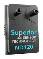
ND120
Pressure Switch, Multi-range, 7 Pressure Ranges, 20 Inch-H2O
⚠️ Reference pricing provided. In case of supply shortages, we will connect you with our trusted procurement partners to ensure your project's continuity.
- Manufacturer: SUPERIOR SENSORS
- Product type: Pressure Switches
- SVHC: To Be Advised
- Port Style: Dual Axial Barbless
- Product Range: ND Series
- Supply Current: 5mA
- Voltage Rating: 3.5V
- Sensor Output Type: I2C Digital, SPI
- Operating Pressure Max: 20Inch-H2O
- Pressure Measurement Type: Differential
| Delivery and price | |
|---|---|
| Units per pack | 100 |
| Price | 20.63 € |
| Current stock | 25+ |
| Lead time | 30 days |
Datasheet

## ND Series

## Differential Pressure Sensors Industrial Applications

- Highly integrated sensor with ADC and DSP

- Up to 7 Selectable Pressure Ranges per Device

- Pressure ranges 0.25 inH2O (62.5 Pa) to 30 inH2O (7500 Pa)

- 16-bit resolution (each selected range)

- Exceptional Zero Stability

- Integrated 50/60Hz Notch Filter

- Selectable Bandwidth Filter from 1.0Hz to 200Hz

- Output Data Rate up to 444Hz

- Total Error Band less than 0.15% FSS

- Very High Accuracy +/- 0.05% of Selected Range

- Long Term Stability +/- 0.05% FSS

- Temperature Compensated -20°C to 85°C

- Supply Voltage Compensation

- Fully Integrated Compensation Math

- Standard I[2] C and SPI Interface

## Product Summary

Based on Superior’s NimbleSense™ architecture, the ND Series family extends the operating temperature down to -20°C and up to 85°C. Additionally, the ND utilizes the company’s proprietary Multi-Range[TM] technology to create the industry’s widest dynamic range. This wider dynamic range offers multiple pressure ranges in a single package thus minimizing the number of sensor variants required to support the demanding functional requirements of the various industrial market segments. For example, one Multi-Range enabled ND Sensor replaces up to 7 competing products, greatly simplifying installation requirements and significantly lowering inventory costs.

performance, the ND Series has incorporated a 50/60Hz notch filter to minimize the impact of power noise spikes. Finally, the ND Series is an excellent choice for applications requiring the utmost reliability.

The ND Series provides a new level of integration combining an advanced piezoresistive sensing element with integrated amplification, ADC, DSP and a digital interface which greatly simplifies customer integration efforts. Advanced digital processing enables new functionality thus simplifying system development, adding manufacturing ease and increasing reliability.

Supporting pressure ranges as low as 0.25 inH2O to as high as 30 inH2O, the ND Series is ideal for a wide variety of industrial applications from air curtains to aeronautics, from environmental chambers to eye surgery equipment, and from UAVs to 3D Printing.

The ND Series measures dry air and non-aggressive gas pressure with very high accuracy and a stable zero point. Non-linearity is also industry leading which is typically 0.05% FSS. The ND Series has a selectable bandwidth filter from 1Hz to 200Hz, and 16-bit resolution. For added

With optional integrated closed loop control customization, advanced digital filtering customization and a 3-mode pressure switch, the ND Series is more than a pressure sensor – it is a complete pressure sensing sub-system.

Constructed with a high reliability plastic enclosure, the ND Series family provides the ideal combination of very high performance and reliability at extended temperature ranges while ensuring customers have a high volume, cost effective solution optimized for a wide array of industrial requirements.

1

www.SuperiorSensors.com

DS-0003D.DOCX

## ND Series

## Industrial Pressure Sensors

## Table of Contents

|1|Maximum Ratings ................................................................ 2|
|---|---|
|2|Suggested Operating Conditions ......................................... 2|
|3|Environmental ..................................................................... 2|
|4|Equivalent Circuit................................................................. 2|
|5|Feature List .......................................................................... 3|
|6|Performance Characteristics ............................................... 3|
|7|Electrical Characteristics ...................................................... 4|
||7.1 Supply Characteristics ................................................. 4|
||7.2 Reset Characteristics .................................................. 4|
||7.3 DAV Characteristics .................................................... 4|
||7.4 I2C Characteristics ...................................................... 4|
||7.5 SPI Characteristics ...................................................... 5|
|8|Materials .............................................................................. 5|
||8.1 Wetted Materials ........................................................ 5|
||8.2 Material Compliance .................................................. 5|
|9|System Overview ................................................................. 6|
|10|Interface .............................................................................. 7|
||10.1 Reset ........................................................................... 7|
||10.2 Communication Interface Selection ........................... 7|
||10.3 SPI Interface ................................................................ 7|
||10.4 I2C Interface ................................................................ 8|
||10.4.1 I2C Address ....................................................... 8|
||10.4.2 I2C Communications Model ............................. 8|
||10.4.3 I2C Clock Stretching .......................................... 9|
||10.4.4 I2C Bus Compatibility ........................................ 9|
||10.5 Extended Data Acquisition ......................................... 9|
||10.5.1 Available Extended Data .................................. 9|
||10.5.2 SPI Extended Data Read ................................... 9|
||10.5.3 I2C Extended Data Read ................................. 10|
||10.6 Control Registers ...................................................... 10|
||10.6.1 Mode Control Register ................................... 10|
||10.6.2 Rate Control Register ..................................... 11|
||10.7 Computing Pressure ................................................. 11|
|11|Mechanical and Manufacturing ......................................... 12|
||11.1 Package Dimensions ................................................. 12|
||11.2 Suggested Pad Layout ............................................... 12|
||11.3 Pinout ....................................................................... 13|
||11.4 Reflow Soldering and Handling Conditions .............. 13|
||11.5 Pick and Place Pick-up Zone ..................................... 13|
||11.6 Packaging Options .................................................... 14|
||11.6.1 Tray Packaging ............................................... 14|
||11.6.2 Tape and Reel ................................................ 15|
||11.7 Part Identification ..................................................... 15|
|12|Packaging Labeling ............................................................ 16|
|13|Ordering Information ........................................................ 16|
|14|Revisions ............................................................................ 17|
|15|Warranty............................................................................ 17|


## 1 Maximum Ratings

|**Parameter**|**Sym**|**Min**|**Max**|**Units**|
|---|---|---|---|---|
|Supply Voltage|VDDM|Gnd-0.3|4.0|V|
|Voltage on I/O Pins<br>VDD> 3.3V<br>VDD≤ 3.3V|VIOML<br>VIOMH|Gnd-0.3<br>Gnd-0.3|5.8<br>VDD+2.5|V<br>V|
|I/O Current|IIOM|-25|25|mA|


## 2 Suggested Operating Conditions

|**Parameter**|**Sym**|**Min**|**Max**|**Units**|
|---|---|---|---|---|
|Supply Voltage|VDDOP|2.8|3.5|V|
|Temperature|TA|-20|85|°C|


## 3 Environmental

|**Parameter**|**Sym**|**Min**|**Max**|**Units**|
|---|---|---|---|---|
|Temperature Range<br>Compensated<br>Operating<br>Storage|TCMP<br>TOP<br>TSTG|-20<br>-20<br>-40|85<br>85<br>85|°C<br>°C<br>°C|
|Humidity<br>(Non-condensing)|RHOP|0|95|% RH|
|Vibration<br>(10Hz-2kHz)|GVIBE|-|15|g|
|Shock (6 ms)|GSHOCK|-|100|g|
|Life|CYLIFE|1M|-|Pressure<br>Cycles|


## 4 Equivalent Circuit

**==> picture [243 x 85] intentionally omitted <==**

**----- Start of picture text -----**<br>
DAV DAV<br>nRST nRST<br>PLOW Port A PLOW Port A<br>MISO/SDA MISO/SDA<br>PHIGH Port B Sensor MOSI/SCL PHIGH Port B Sensor MOSI/SCL<br>(SPI) SCK (I [2] C) SCK VI2C Address<br>nSS nSS<br>VDD VDD<br>Gnd Gnd<br>**----- End of picture text -----**<br>


2

www.SuperiorSensors.com

DS-0003D.DOCX

## ND Series

## Industrial Pressure Sensors

## 5 Feature List

|**Parameter**|**Sym**<br>~~Gs~~|**ND210**|**ND110**|**ND120**|**ND130**|**Units**|**Notes**|
|---|---|---|---|---|---|---|---|
|Number of FS Pressure Ranges<br>~~ee~~|PNUM<br>~~ee~~<br>~~Gs~~|7<br>~~ee~~|6<br>~~ee~~|7<br>~~ee~~|6<br>~~ee~~|Each<br>~~ee~~|~~ee~~|
|Specified FS Range Extents<br>~~ne~~|PEXT<br>~~Gs~~<br>~~ne~~|±0.25 to ±10<br>~~ne~~|±0.5 to ±10<br>~~ne~~|±1.0 to ±20<br>~~ne~~|±2.0 to ±30<br>~~ne~~|inH2O<br>~~ne~~|~~ne~~|
|Number of BW Filter Corners<br>~~ee~~|BWNUM<br>~~ee~~|8<br>~~ee~~||||Each<br>~~ee~~|~~ee~~|
|BW Corner Frequency Extents<br>~~ne~~|fBWEXT<br>~~ne~~|1.0 to 200<br>~~ne~~||||Hz<br>~~ne~~|~~ne~~|
|Common Mode Pressure<br>~~ne~~|PCM<br>~~ne~~|500<br>~~ne~~|500<br>~~ne~~|500<br>~~ne~~|700<br>~~ne~~|inH2O<br>~~ne~~|1<br>~~ne~~|
|Proof Pressure<br>~~ne~~|PPROOF<br>~~ne~~<br>~~Ge~~|40<br>~~ne~~|40<br>~~ne~~|40<br>~~ne~~|100<br>~~ne~~|inH2O<br>~~ne~~|2<br>~~ne~~|
|Burst Pressure<br>~~ee~~|PBURST<br>~~ee~~<br>~~Ge~~|120<br>~~ee~~|120<br>~~ee~~|120<br>~~ee~~|200<br>~~ee~~|inH2O<br>~~ee~~|3<br>~~ee~~|


1) Pressure applied to both ports simultaneously without incurring part damage.

2) Pressure at which the sensor will not suffer permanent damage.

- 3) Pressure if exceeded could cause permanent damage to the sensor.

## 6 Performance Characteristics

|**Parameter**<br>~~LL~~<br>~~ee~~<br>~~ee~~|**Sym**<br>~~C~~<br>~~LL~~<br>~~es~~|**ND210**<br>~~CC~~<br>~~I~~<br>~~LL~~<br>~~eae~~|**ND110/ND120/ND130**<br>~~J~~<br>~~LL~~<br>~~eae~~|**Units**<br>~~LL~~|**Notes**<br>~~LL~~|
|---|---|---|---|---|---|
|||**Min**<br>**Typ**<br>**Max**<br>~~CC~~<br>~~I~~<br>~~LL~~<br>~~eae~~|**Min**<br>**Typ**<br>**Max**<br>~~J~~<br>~~LL~~<br>~~eae~~|||
|Accuracy<br>~~LL~~<br>~~ee~~<br>~~ee~~|PACC<br>~~LL~~<br>~~es~~|-<br>0.05<br>0.2<br>~~LL~~<br>~~eae~~|-<br>0.05<br>0.2<br>~~LL~~<br>~~eae~~|% RNG<br>~~LL~~|1, 2<br>~~LL~~|
|Total Error Band<br>~~ee~~<br>~~ee~~|TEB<br>~~es~~|-<br>0.10<br>0.3<br>~~eae~~|-<br>0.15<br>0.75<br>~~eae~~|% FSS|3|
|TEB After AZ<br>~~ee~~<br>~~a~~<br>~~ee~~|TEBAZ<br>~~es~~|-<br>0.07<br>0.2|-<br>0.10<br>0.5|% FSS|7|
|Long Term Stability<br>~~ee~~<br>~~ee~~|LTS<br>~~es~~|-<br>0.10<br>0.25<br>~~a~~|-<br>0.15<br>0.35<br>~~a~~|% FSS/YR1<br>~~a~~|8<br>~~a~~|
|Thermal Hysteresis<br>~~ee~~<br>~~ee~~<br>~~ee~~|THYS<br>~~es~~<br>~~es~~|-<br>0.05<br>-<br>~~a~~<br>~~a~~|-<br>0.075<br>-<br>~~a~~<br>~~a~~|% FSS<br>~~a~~<br>~~a~~|~~a~~<br>~~a~~|
|Pressure Hysteresis<br>~~ee~~<br>~~ee~~<br>~~ee~~|PHYS<br>~~es~~<br>~~es~~<br>~~es~~|-<br>0.05<br>-<br>~~a~~<br>~~a~~<br>~~a~~|-<br>0.05<br>-<br>~~a~~<br>~~a~~<br>~~a~~|% RNG<br>~~a~~<br>~~a~~<br>~~a~~|1<br>~~a~~<br>~~a~~<br>~~a~~|
|Position Sensitivity<br>~~ee~~<br>~~ee~~<br>~~ee~~|PPS<br>~~es~~<br>~~es~~<br>~~es~~|-<br>0.25<br>-<br>~~a~~<br>~~a~~<br>~~a~~|-<br>2.0<br>-<br>~~a~~<br>~~a~~<br>~~a~~|Pa<br>~~a~~<br>~~a~~<br>~~a~~|~~a~~<br>~~a~~<br>~~a~~|
|Supply Rejection<br>~~ee~~<br>~~ee~~<br>~~ee~~|PSR<br>~~es~~<br>~~es~~<br>~~es~~|-<br>0.0005<br>-<br>~~a~~<br>~~a~~<br>~~a~~|-<br>0.0005<br>-<br>~~a~~<br>~~a~~<br>~~a~~|Pa/mV<br>~~a~~<br>~~a~~<br>~~a~~|~~a~~<br>~~a~~<br>~~a~~|
|Resolution<br>~~ee~~<br>~~ee~~<br>~~ee~~|RES<br>~~es~~<br>~~es~~<br>~~es~~|-<br>16<br>-<br>~~a~~<br>~~a~~<br>~~a~~|-<br>16<br>-<br>~~a~~<br>~~a~~<br>~~a~~|bit<br>~~a~~<br>~~a~~<br>~~a~~|4<br>~~a~~<br>~~a~~<br>~~a~~|
|System ENOB<br>~~ee~~<br>~~ee~~|ENOB<br>~~es~~<br>~~es~~|-<br>17<br>-<br>~~a~~<br>~~a~~<br>~~a~~|-<br>17<br>-<br>~~a~~<br>~~a~~|BitRMS<br>~~a~~<br>~~a~~|5<br>~~a~~<br>~~a~~|
|Data Update Rate<br>~~ee~~<br>~~ee~~|fUPDATE<br>~~es~~<br>~~ee~~|432<br>444<br>456<br>~~a~~<br>~~ee~~<br>~~a~~|432<br>444<br>456<br>~~a~~<br>~~ee~~|Hz<br>~~a~~<br>~~ee~~|6<br>~~a~~<br>~~ee~~|


2) Uncertainty limited by system noise for ranges of 0.5 inH2O and below.

- 3) Includes errors of offset, span, hysteresis and thermal effects.

- 4) Each selected range has the specified resolution

- 5) ENOB stated for fBW set to 1.0 Hz.

6) The internal update rate is fixed and does not change with range or filter settings. Sampling at lower data rates are possible provided the Nyquist frequency is observed. It is suggested to sample at least 3x the set fBW frequency.

- 7) Total error band within 24 hours of a sensor auto-zero. Includes all error components of TEB.

- 8) YR1 is the first year.  The most significant drift occurs during the first year and is lessened for each subsequent year. For each subsequent year, use 25% of the prior years' drift figure to estimate the drift for that specific year.

3

DS-0003D.DOCX

Industrial Pressure Sensors

## ND Series

## 7 Electrical Characteristics

## 7.1 Supply Characteristics

|**Parameter**|**Sym**|**ND210**|**ND110/ND120/ND130**|**Units**|**Notes**|
|---|---|---|---|---|---|
|||**Min**<br>**Typ**<br>**Max**|**Min**<br>**Typ**<br>**Max**|||
|Supply Current|IDD|-<br>6.0<br>6.5|-<br>5.0<br>5.5|mA||
|Supply Capacitance|CDD|-<br>10<br>-|-<br>10<br>-|uF|1|


1) Supply capacitance is provided within the part however it is recommended to include a 0.1 uF decoupling cap near the supply pads.

## 7.2 Reset Characteristics

|**Parameter**<br>~~Le~~<br>~~a~~|**Sym**<br>~~Le~~<br>|**Condition**<br>~~Le~~<br>|**All ND Series Parts**<br>~~Le~~<br>~~ee~~<br>|**Units**<br>~~Le~~<br>~~ee_L~~<br>|**Notes**<br>~~Le~~<br>~~_L~~<br>|
|---|---|---|---|---|---|
||||**Min**<br>**Typ**<br>**Max**<br>~~Le~~<br>~~ee~~<br>|||
|Power-On Reset<br>Threshold<br>~~Le~~<br>~~a~~<br>~~a~~<br>~~a~~|VPORR<br>VPORF<br>~~Le~~<br>~~ee~~<br>~~ee~~|Rising Voltage on VDD<br>FallingVoltage on VDD<br>~~Le~~<br>~~ee~~<br>~~eeee~~|-<br>0.75<br>1.4<br>-<br>-<br>1.36<br>~~Le~~<br>~~ee~~<br>~~ee~~<br>~~ee~~|V<br>V<br>~~Le~~<br>~~ee_L~~<br>~~ee~~<br>~~ee~~<br>~~ee~~|~~Le~~<br>~~_L~~<br>~~ee~~<br>~~ee~~|
|Interface Detect<br>Delay<br>~~a ~~<br>~~a~~<br>~~a~~<br>~~ee~~|tIOD<br> ~~ee~~<br>~~ee~~<br>~~ee~~<br>|From POR or External<br>Reset<br>~~ee~~<br>~~eeee~~<br>~~eeee~~|-<br>-<br>40<br>~~ee~~<br>~~ee~~<br>~~ee~~<br>~~ee~~|ms<br>~~ee _L~~<br>~~ee~~<br>~~ee~~<br>~~ee~~<br>~~ee~~<br>~~ee~~|~~_L~~<br>~~ee~~<br>~~ee~~<br>~~ee~~|
|First Response<br>SettlingTime<br>~~a~~<br>~~a~~<br>~~ee~~<br>~~ee~~|tFRD<br>~~ee ~~<br>~~ee~~<br>~~es~~<br>|From POR or External<br>Reset<br> ~~eeee~~<br>~~eeee~~<br>|-<br>-<br>80<br>~~ee~~<br>~~ee~~|ms<br>~~ee~~<br>~~ee~~<br>~~ee~~<br>~~ee~~|1<br>~~ee~~<br>~~ee~~|
|External Reset Low<br>~~ee~~<br>~~ee~~<br>~~ee~~|tRSTL<br>~~ee~~<br>~~es~~<br>~~es en~~|~~eeee~~<br>~~en~~|15<br>-<br>-<br>~~ee~~|us<br>~~ee~~<br>~~ee~~|~~ee~~|
|Input High Voltage<br>~~ee ~~<br>~~ee~~<br>~~ee~~|VIH<br> ~~es~~<br>~~es en~~|~~en~~|VDD-0.6<br>-<br>-|~~ee~~|2|
|Input Low Voltage<br> <br>~~ee ~~<br>~~ee~~<br>~~ee~~|VIL<br> ~~es~~<br> ~~es en~~|~~en~~|-<br>-<br>0.6<br>~~ee~~|~~ee~~|2<br>~~ee~~|
|Internal Pull-Up<br>Current<br> <br>~~ee~~<br>~~a~~<br>~~ee~~|IPU<br> ~~es en~~<br>~~ee~~|VIN= 0V<br>~~en~~<br>~~ee~~|-<br>-10<br>-30<br>~~ee~~<br>~~ee~~|uA<br>~~ee~~<br>~~ee~~|2<br>~~ee~~<br>~~ee~~|
|Input Capacitance<br>~~a ~~<br>~~ee~~|CIN<br> ~~ee~~|~~ee~~|-<br>7<br>-<br>~~ee~~<br>~~ee~~|pF<br>~~ee~~<br>~~ee~~|2<br>~~ee~~<br>~~ee~~|


## 7.3 DAV Characteristics

|**Parameter**|**Sym**|**Condition**|**All ND Series Parts**|**Units**|**Notes**|
|---|---|---|---|---|---|
||||**Min**<br>**Typ**<br>**Max**|||
|Output High Voltage|VOH|IO= -3 mA|VDD-0.7<br>-<br>-|V||
|Output Low Voltage|VOL|IO= 8 mA|-<br>-<br>0.6|V||


## 7.4 I2C Characteristics

|**Parameter**|**Sym**|**Condition**|**All ND Series Parts**|**Units**|**Notes**|
|---|---|---|---|---|---|
||||**Min**<br>**Typ**<br>**Max**|||
|SCL Clock Frequency|fSCL||100<br>-<br>400|kHz||
|Clock Stretch Time|tCKSTR||-<br>15<br>100|us||
|Input High Voltage|VIH||VDD-0.6<br>-<br>-|||
|Input Low Voltage|VIL||-<br>-<br>0.6|||
|Output Low Voltage|VOL|IO= 8 mA|-<br>-<br>0.6|V||
|Input Capacitance|CIO||-<br>7<br>-|pF||


4

www.SuperiorSensors.com

DS-0003D.DOCX

## ND Series

## Industrial Pressure Sensors

7.5 SPI Characteristics

|**Parameter**<br>~~|~~<br>~~es~~|**Sym**<br>~~|~~<br>~~es~~|**Condition**<br>~~|~~|**All ND Series Parts**<br>~~|~~|**Units**<br>~~|~~|**Notes**<br>~~|~~|
|---|---|---|---|---|---|
||||**Min**<br>**Typ**<br>**Max**<br>~~|~~|||
|Output High Voltage<br>~~es~~<br>~~es~~|VOH<br>~~es~~<br>~~es~~|IO= -3 mA<br>~~ns~~|VDD-0.7<br>-<br>-|V|1|
|Output Low Voltage<br>~~es~~<br>~~es~~<br>~~es~~|VOL<br>~~es~~<br>~~es~~<br>~~es~~|IO= 8 mA<br>~~ns~~<br>~~ns~~|-<br>-<br>0.6|V|1|
|Input High Voltage<br>~~es ~~<br>~~es~~<br>~~es~~|VIH<br> ~~es~~<br>~~es~~<br>~~es~~|~~ns~~<br>~~ns~~<br>~~ns~~|VDD-0.6<br>-<br>-||2, 3|
|Input Low Voltage<br>~~es ~~<br>~~es~~<br>~~a~~|VIL<br> ~~es~~<br>~~es~~<br>~~ee~~|~~ns~~<br>~~ns~~<br>~~ee~~|-<br>-<br>0.6<br>~~ee~~|~~ee~~|2, 3|
|Internal Pull-Up<br>Current<br>~~es ~~<br>~~a~~<br>~~ee~~|IPU<br> ~~es~~<br>~~ee~~<br>~~ee~~|VIN= 0V<br>~~ns~~<br>~~ee~~<br>~~ee~~|-<br>-10<br>-30<br>~~ee~~<br>~~ee~~|uA<br>~~ee~~<br>~~ee~~|2, 3<br>~~ee~~|
|Time nSS to First<br>SCK Edge<br>~~a~~<br>~~ee~~<br>~~es~~|tSC<br>~~ee ~~<br>~~ee~~<br>~~es~~|~~ee~~<br>~~ee~~<br>~~ns~~|100<br>-<br>-<br>~~ee ~~<br>~~ee~~|us<br> ~~ee~~<br>~~ee~~|~~ee~~|
|Clock Cycle Time<br>~~ee ~~<br>~~es~~<br>~~a~~<br>~~a~~|tCC<br> ~~ee~~<br>~~es~~<br>~~a~~|~~ee~~<br>~~ns~~<br>~~ee~~|6<br>-<br>-<br>~~ee~~<br>~~ee~~|us<br>~~ee~~<br>~~ee~~<br>~~ee~~|~~ee~~<br>~~ee~~|
|Byte to Byte Cycle<br>Time<br>~~es ~~<br>~~a~~<br>~~a~~<br>~~es~~|tBC<br> ~~es~~<br>~~a~~<br>~~ee ee~~<br>|~~ns~~<br>~~ee~~<br>~~ee~~|100<br>-<br>-<br>~~ee~~<br>~~ee~~|us<br>~~ee~~<br>~~ee~~<br>~~ee~~<br>~~ee~~|~~ee~~<br>~~ee~~|
|Time Last Clock to<br>nSS High<br>~~a~~<br>~~a~~<br>~~es~~<br>~~es~~|tCN<br>~~a~~<br>~~ee ee~~<br>~~**es**~~|~~ee~~<br>~~ee~~<br>~~**n**n~~|20<br>-<br>-<br>~~ee~~<br>~~ee~~|us<br>~~ee~~<br>~~ee~~<br>~~ee~~<br>~~ee~~|~~ee~~<br>~~ee~~|
|Cycle Time nSS<br>~~es~~<br>~~es~~|tCS<br>~~ee ee~~<br>~~**es**~~|~~ee~~<br>~~**n**n~~<br>~~s~~|6<br>-<br>-<br>~~ee~~|us<br>~~ee~~<br>~~ee~~|~~ee~~|
|Input Capacitance<br>~~es ~~<br>~~es~~|CIN<br> ~~**es**~~|~~**n**n~~<br>~~s~~|-<br>7<br>-|pF<br>~~ee~~|2|


## 8 Materials

## 8.1 Wetted Materials

|**Parameter**|**Sym**|**ND210**|**ND210**|**ND110/ND120/ND130**|**ND110/ND120/ND130**|**Units**|**Notes**|
|---|---|---|---|---|---|---|---|
|||**PA**|**PB**|**PA**|**PB**|||
|Wetted Materials|MATWET|Epoxy<br>Nylon<br>RTV<br>Silicon<br>Gold<br>Aluminum|Epoxy<br>Nylon<br>RTV<br>Silicon<br>Gold<br>Aluminum|Epoxy<br>Nylon<br>RTV<br>Silicon|Epoxy<br>Nylon<br>RTV<br>Silicon<br>Gold<br>Aluminum|||


## 8.2 Material Compliance

|**Parameter**|**Sym**|**All ND Series Parts**|**Units**|**Notes**|
|---|---|---|---|---|
|RoHS|REGRoHS|RoHS Compliant|||
|REACH|REGREAC|REACH Compliant|||


5

www.SuperiorSensors.com

DS-0003D.DOCX

## ND Series

## Industrial Pressure Sensors

## 9 System Overview

The ND Series pressure sensor is a fully integrated pressure acquisition system in a sensor module. The acquisition system includes anti-alias filters, data acquisition, 50/60Hz notch filter, sensor compensation, bandwidth limiting and I/O functions. Refer to the figure below for the ND Series block diagram.

**==> picture [498 x 180] intentionally omitted <==**

**----- Start of picture text -----**<br>
User Control Registers<br>Pressure Anti-Alias  Δ-Sigma  Mode Control Rate Control<br>Sensor Filter Modulator<br>DAV<br>1b Enable 3b Range Control 3b BW Control ControllerRate  InterfaceHW  nRST<br>Va Anti-Alias  Δ-Sigma<br>Filter Modulator MISO/SDA<br>o y Decimation 4 50/60HzNotch | 4 CompensationFPU with 4 BW LimitIIR tp SPI/I [2] C  MOSI/SCLSCK<br>(Sinc [2] ) Linearization (2 [nd]  Order) Interface nSS<br>T [o] SAR ADC<br>5 ) pO<br>26 Term<br>Compensation<br>| Coefficients<br>Vs<br>SAR ADC<br>MCU<br>O—< _<br>**----- End of picture text -----**<br>


**==> picture [4 x 22] intentionally omitted <==**

**----- Start of picture text -----**<br>
FIG-0011A<br>**----- End of picture text -----**<br>


There are also two user controlled registers that tune the sensor to the specific user requirements.  The first register is the Mode Control register that determines the output pressure range, the corner frequency of the bandwidth limiting filter and enables or disables the 50/60Hz notch filter.

The second register is the Rate Control register which controls the rate at which the Data Available (DAV) pin is asserted. The internal sensor data update rate of 444 Hz is often much faster than industrial requirements so the Rate Control register can throttle down the rate at which the Data Available pin (DAV) is asserted. The DAV is reset upon each read of the pressure sensor. An internal model of the Rate Controller is illustrated in the figure to the right.

**==> picture [280 x 106] intentionally omitted <==**

**----- Start of picture text -----**<br>
Rate Control<br>Register<br>Reload Value<br>Internal Update  Zero DAV<br>Down Counter S Q<br>(fUPDATE)<br>Data Read<br>R FIG-0012B<br>**----- End of picture text -----**<br>


6

www.SuperiorSensors.com

DS-0003D.DOCX

## ND Series

## Industrial Pressure Sensors

## 10 Interface

## 10.1 Reset

Reset timing is shown in the diagram below.

The communications method (SPI or I[2] C) is established during the time just after reset. During this time (tIOD), no communications should take place.

Also, the internal filters are settling during the time tFRD and data acquired during this time may not be fully settled.

**==> picture [412 x 194] intentionally omitted <==**

**----- Start of picture text -----**<br>
 Reset Timing Diagram<br>VDD VPORR VPORF<br>Internal Reset<br>—| tRSTL<br>_RST<br>—| tIOD tIOD<br>Communications<br>Available<br>tFRD tFRD<br>Filters Settled<br>FIG-0021A<br>**----- End of picture text -----**<br>


## 10.2 Communication Interface Selection

The communications interface is selected by interrogating the nSS pin after the internal power on reset delay. If nSS is high, the SPI interface will be selected otherwise (if low) the I[2] C interface will be selected. Grounding the nSS pin is an acceptable method for selecting the I[2] C interface. NOTE: The I[2] C interface supports 10 interface addresses. Refer to section 10.4.1 for the details on I[2] C address selection.

## 10.3 SPI Interface

The SPI interface uses a 16 bit transfer for all communications. Data is MSB first for both MOSI and MISO data transfers. Refer to the figure below for specific timing requirements.

**==> picture [459 x 125] intentionally omitted <==**

**----- Start of picture text -----**<br>
 SPI Timing Diagram<br>tsc tcc tbc tcn tcs<br>SCK LITOL LL LS LU LU WLS LI LS LU UW LW<br>MOSI AANA Bit 7 CD Bit 6 Bit 5  CD CD Bit 4 Bit 3 CRED Bit 2  CGD Bit 1  CGD Bit 0  CGD CGD Bit 7 CGEREED Bit 6 GGEEEED Bit 5 CGD Bit 4 GGRREEED Bit 3 CGRREEEED Bit 2  CHRD Bit 1 GERRI Bit 0 NV 0 00/010 000 000A<br>MISO L Bit 7 Bit 6 Bit 5 Bit 4 egg Bit 3 Bit 2 Bit 1 Bit 0 Bit 7 Bit 6 Bit 5 Bit 4 Bit 3 Bit 2 Bit 1 s Bit 0<br>nSS a aE FIG-0013A<br>**----- End of picture text -----**<br>


The data communications has been reduced to a simple 16 bit transfer model for reading the pressure output. Each communication cycle consists of master sending the Mode and Rate data to be placed into the sensor Mode Register and Rate Registers respectively. Simultaneously, the sensor sends the pressure data for the master to receive. Refer to the figure below for the data communication model of the ND Series sensor.

7

www.SuperiorSensors.com

DS-0003D.DOCX

## ND Series

## Industrial Pressure Sensors

The requirement to send the Mode and Rate bytes on each data read cycle is intentional. The purpose is to force the master to send specific data for each communication and prevent inadvertent data from being sent to the sensor. Since a SPI interface will generally re-circulate data through its shift register, the intention is to prevent the pressure output from the sensor from being re-circulated back to the sensor and potentially causing unintended corruption of the intended mode register.

**==> picture [459 x 111] intentionally omitted <==**

**----- Start of picture text -----**<br>
 SPI Data Diagram<br>SCK — TT LI LI LI LI LU LI LU We_tJLU UW UW WWW WLW LW _<br>MOSI  User Mode Byte  User Rate Byte<br>MISO eeniD OD, Pressure Output High Byte CD Pressure Output Low Byte CD el<br>nSS ia FIG-0014A<br>**----- End of picture text -----**<br>


## 10.4 I[2] C Interface

The ND Series is compatible with the I[2] C protocol. For detailed information regarding the I[2] C protocol, please refer to the Philips I[2] C Bus Specification, Version 2.

## 10.4.1 I[2] C Address

|I2C Address Selection Table|I2C Address Selection Table|I2C Address Selection Table|I2C Address Selection Table|
|---|---|---|---|
|R1 (kΩ)|R2 (kΩ)|Address<br>(decimal)|Address<br>)<br>Address<br>(hex)|
|120|5.6|49|0x31|
|120|12|48|0x30|
|120|27|47|0x2F|
|120|51|46|0x2E|
|120|100|45|0x2D|
|56|100|44|0x2C|
|30|100|43|0x2B|
|15|100|42|0x2A|
|5.6|100|41|0x29|
|0|NoPop|40|0x28|


The I[2] C address is set to 0x28 by grounding the SCK line. Other I[2] C addresses can be established by applying a voltage to the SCK line by use of a resistor divider across the sensor supply voltage. The suggested resistor values and the respective I[2] C address are shown in the table to the left.

Note: R1 is the lower resister of the divider where R2 is the upper resistor of the divider.

## 10.4.2 I[2] C Communications Model

The sensor is configured as a slave device and as such, the communicating host must be configured as a master. There are two types of possible data transfers, data transfers from the master transmitter to an addressed sensor (WRITE), and data transfers from an addressed sensor to a master receiver (READ).  The master device initiates both types of data transfers and provides the serial clock pulses on SCL.

The communications model for I[2] C is similar to that of SPI however, since I[2] C is a half-duplex protocol, the transfer of information to and from the sensor is separated into two separate communications. This is in contrast to the SPI interface where the transmitted and received data occurs simultaneously to and from the host. Refer to the figure to the right for the data communication model for the ND Series sensors.

**==> picture [77 x 7] intentionally omitted <==**

**----- Start of picture text -----**<br>
  I [2] C Communication Model<br>**----- End of picture text -----**<br>


**==> picture [266 x 162] intentionally omitted <==**

**----- Start of picture text -----**<br>
(1) Setting Mode Control Register Only<br>Slave Address [6:0] Write DataByte 1<br>User Mode Byte [7:0]<br>(2) Setting Both Control Registers<br>Slave Address [6:0] Write DataByte 1 Data Byte 2<br>User Mode Byte [7:0] User Rate Byte [7:0]<br>(3) Reading Pressure Data<br>Slave Address [6:0] Read DataByte 1 Data Byte 2<br>Pressure Output [15:8] Pressure Output [7:0]<br>Bits generated by Master Bits generated by Sensor<br>Start A6 A5 A4 A3 A2 A1 A0 0 ACK D7 D6 D5 D4 D3 D2 D1 D0 ACK Stop<br>Start A6 A5 A4 A3 A2 A1 A0 0 ACK D7 D6 D5 D4 D3 D2 D1 D0 ACK D7 D6 D5 D4 D3 D2 D1 D0 ACK Stop<br>Start A6 A5 A4 A3 A2 A1 A0 1 ACK D15 D14 D13 D12 D11 D10 D9 D8 ACK D7 D6 D5 D4 D3 D2 D1 D0 NACK Stop<br>**----- End of picture text -----**<br>


8

www.SuperiorSensors.com

DS-0003D.DOCX

## ND Series

## Industrial Pressure Sensors

## 10.4.3 I[2] C Clock Stretching

The figure to the right illustrates the I[2] C 12C Clock Stretching clock stretching by the sensor. At times, the sensor requires additional time to respond to the host and utilizes the clock stretching oe LE feature of the I[2] C protocol. This is accomplished by holding the SCL low after the ACK cycle of a data transfer. Refer to Section 7.4 for the clock stretching timing. Note, the maximum clock stretch time will generally only occur once during the three ACK cycles of a two byte transfer. That is, the balance of ACK's during a multi-byte transfer will generally include the typical clock stretching time.

## 10.4.4 I[2] C Bus Compatibility

The I[2] C specification allows any recessive voltage between 3.0 and 5.0 V. Different devices on the bus may operate at different voltage levels. However, the maximum voltage on any port pin must conform to the electrical characteristics specifications (See section 1). The bi-directional SCL (serial clock) and SDA (serial data) lines must be connected to a positive power supply voltage through a pull-up resistor or similar circuit. Every device connected to the bus must have an open-drain or open-collector output for both the SCL and SDA lines, so that both are pulled high (recessive state) when the bus is free.

## 10.5 Extended Data Acquisition

## 10.5.1 Available Extended Data

For either the SPI or I[2] C interface, additional data is available beyond the pressure. The means to access this extended data is to continue reading data (either SPI or I[2] C) beyond the first 16 bits of pressure information. The following table defines the order of the available data and respective format.

|**Data**|**Bytes**|**Format**|**Interpretation**|**Example**|
|---|---|---|---|---|
|Pressure|1-2|2 byte, Signed Int|See Section 10.7|See Section 10.7|
|Temperature|3-4|2 byte, Signed Int|Fixed Decimal [8.8 bits], Upper 8<br>bits integer, lower 8 bits<br>fractional. Temperature in °C|1880H (18.80H) = 24.5°C|
|Model|5-12|8 byte, ASCII, null<br>terminated|Right reading ASCII with null<br>termination|4EH,44H,32H,31H,30H,00H,xxH,xxH = ND210<br>4EH,44H,30H,30H,35H,44H,00H,xxH = ND005D|
|Serial Number|13-16|4 byte, Hex|Unique 4 byte serial for each part|2FD627A4H|
|Build Number|17-22|6 byte, ASCII, null<br>terminated|Right reading ASCII with null<br>termination|30H,30H,30H,33H,43H,00H = 0003C|


## 10.5.2 SPI Extended Data Read

Reading the extended data while using the SPI interface is the same as shown in Section 10.3 with exception that the master continues to read during the same nSS sequence to read all 22 bytes of the extended data. Any portion of the 22 bytes can be read during the transfer. That is, for example, 4 bytes could be read to acquire only the pressure and temperature information.  When reading the extended data, only the first two bytes sent to the sensor (User Mode and User Rate) are used to set the internal registers. The subsequent bytes (bytes 5 through 22) are ignored. Data read following the first 22 bytes is undefined.

9

www.SuperiorSensors.com

DS-0003D.DOCX

## ND Series Industrial Pressure Sensors

## 10.5.3 I[2] C Extended Data Read

Reading the extended data via the I[2] C interface is similar to using the SPI interface where the master can simply continue to reading the sensor during the pressure reading transfer. The master continues Ack'ing until the number of desired bytes are read.

## 10.6 Control Registers

**==> picture [109 x 9] intentionally omitted <==**

**----- Start of picture text -----**<br>
 Mode Control Register Detail<br>**----- End of picture text -----**<br>


10.6.1 Mode Control Register Default Value: 0xF6 Details of the Mode Control register are illustrated in the figure to the right. ~~——~~

**==> picture [181 x 85] intentionally omitted <==**

**----- Start of picture text -----**<br>
Mode Register (General)<br>b7 b6 b5 b4 b3 b2 b1 b0<br>Too<br>Pressure Range Select<br>I/O Watchdog Enable<br>BW Limit Select<br>Notch Enable<br>— _ ——<br>**----- End of picture text -----**<br>


## Bits 0-2 control the output pressure range.

Bit 3 is the I/O Watchdog Enable bit. When set, the I/O watchdog is enabled. When enabled, the I/O watchdog will monitor the I/O activity. If I/O activity is not detected for the I/O Watchdog timeout time, the pressure sensor will reset itself. The I/O watchdog timeout time is determined by the currently active bandwidth setting.

|Bit 3 is the I/O Watchdog Enable bit. When set,<br>the I/O watchdog is enabled. When enabled, the<br>I/O watchdog will monitor the I/O activity. If I/O<br>activity is not detected for the I/O Watchdog|~~—~~_~~——~~|~~—~~_~~——~~|~~—~~_~~——~~|~~—~~_~~——~~|~~—~~_~~——~~|~~—~~_~~——~~|~~—~~_~~——~~|~~—~~_~~——~~|~~—~~_~~——~~|~~—~~_~~——~~|~~—~~_~~——~~|~~—~~_~~——~~|~~—~~_~~——~~|~~—~~_~~——~~|~~—~~_~~——~~|~~—~~_~~——~~|~~—~~_~~——~~|~~—~~_~~——~~|~~—~~_~~——~~|~~—~~_~~——~~|BW Limit Select<br>Notch Enable<br>~~——~~|~~——~~|||
|---|---|---|---|---|---|---|---|---|---|---|---|---|---|---|---|---|---|---|---|---|---|---|---|---|
|activity is not detected for the I/O Watchdog<br>timeout time, the pressure sensor will reset<br>itself. The I/O watchdog timeout time is|b7<br>b6<br>b5<br>b4<br>b3<br>b2<br>b1<br>b0<br>Mode Register (Detail)<br>Por||||||||||||||||||||||||
|determined by the currently active bandwidth|||||||||||||||||||||||||
|setting.|||||||||||||||||||||Pressure Range Select (by Model)||||
||||||||||||||||||||||ND110<br>ND210||ND120<br>ND130|ND005D|
|Bits 4-6 control the BW Limit Filter.|||||||||||||||0|0||0|||0.5 inH2O<br>0.25 inH2O||1.0 inH2O<br>2.0 inH2O|0.5 psi|
|Bit 7 is the Notch Filter Enable bit. When|||||||||||||||0|0||1|||0.5 inH2O<br>0.25 inH2O||1.0 inH2O<br>2.0 inH2O|0.5 psi|
|enabled, the 50/60Hz notch filter is active.|||||||||||||||0|1||0|||0.5 inH2O<br>0.5 inH2O||2.0 inH2O<br>2.0 inH2O|0.5 psi|
||||||||||||||||0|1||1|||1.0 inH2O<br>1.0 inH2O||4.0 inH2O<br>4.0 inH2O|0.8 psi|
||||||||||||||||1|0||0|||2.0 inH2O<br>2.0 inH2O||5.0 inH2O<br>5.0 inH2O|1.0 psi|
|Please note the available pressure ranges for the|||||||||||||||1|0||1|||4.0 inH2O<br>4.0 inH2O||10.0 inH2O<br>10.0 inH2O|2.0 psi|
|different sensor models are indicated in the|||||||||||||||1|1||0|||5.0 inH2O<br>5.0 inH2O||15.0 inH2O<br>20.0 inH2O|4.0 psi|
|table. For values where the pressure range is not<br>available for the given sensor (high or low), the|||||||||||||||1|1||1|||10.0 inH2O<br>10.0 inH2O||20.0 inH2O<br>30.0 inH2O|5.0 psi|
|table is highlighted in light orange and indicates<br>the given full scale value to use for pressure<br>conversion. It is possible to use these values.<br>It should also be noted that upon changing the<br>Mode Control value, there is a one cycle latency<br>before the new Mode Control value becomes<br>valid. That is, the data of the communication<br>cycle following a change to the Mode Control<br>register will not reflect the change. It is not until<br>the second communication cycle that the change<br>in the Mode Control register will be reflected in<br>the output data.||||0<br>0<br>0<br>0<br>1<br>1<br>1<br>1|||0<br>0<br>1<br>1<br>0<br>0<br>1<br>1||Disabled<br>0<br>1<br>0<br>1<br>0<br>1<br>0<br>1<br>1.0 Hz<br>2.0 Hz<br>5.0 Hz<br>10 Hz<br>20 Hz<br>50 Hz<br>100 Hz<br>200 Hz<br>BW Limit Select<br>1 sec<br>500 ms<br>200 ms<br>200 ms<br>200 ms<br>200 ms<br>200 ms<br>I/O Watchdog Timeout<br>0<br>1<br>Enabled<br>I/O Watchdog Enable<br>200 ms<br>~~EE~~||||||||||||||||
||0<br>1<br>A|||||||||||||||||||Notch Filter Disabled<br>Notch Filter Enabled<br>Notch Enable<br>~~—~~|||||


10

www.SuperiorSensors.com

DS-0003D.DOCX

## ND Series

## Industrial Pressure Sensors

## 10.6.2 Rate Control Register

## Default Value: 0x00

The Rate Control Register controls the rate at which the DAV pin is asserted indicating new data is available. This register is primarily used to throttle down the actual data transfer rate (when using the DAV as the trigger to sample) since the general industrial requirement is less than the internal 444 Hz update rate.

The function of this register is that it is the reload value of a data rate counter. The value of the Rate Control Register is the divisor of the 444 Hz internal data rate. Since a divisor of zero is not possible, a zero value will select the auto-select rate mode. In this mode, the rate is selected based on the selected bandwidth limit. The auto rate value is roughly 3x the corner frequency of the selected bandwidth limit in all auto selected rates (where possible).

Note: Start-up time for the sensor is approximately 80ms for the first sample to be settled. Requesting data during this time will result in invalid information. However, this start-up time can be used for configuring the Mode and Rate registers by performing a transfer with the desired Mode and Rate register values and discarding the received pressure data. After waiting the required start-up time, the sensor will respond with desired data since the Mode and Rate registers have been pre-established.

## Rate Control Register Detail

**==> picture [232 x 283] intentionally omitted <==**

**----- Start of picture text -----**<br>
Rate Control Register<br>b7 b6 b5 b4 b3 b2 b1 b0<br>0 0 0 0 0 0 0 0 Auto Select<br>0 0 0 0 0 0 0 1 444 Hz<br>0 0 0 0 0 0 1 0 222 Hz<br>0 0 0 0 0 0 1 1 148 Hz<br>1 1 1 1 1 1 1 0 1.75 Hz<br>1 1 1 1 1 1 1 1 1.74 Hz<br>Selected BW Limit Auto Select Rate<br>1.0 Hz 3.0 Hz<br>2.0 Hz 6.0 Hz<br>5.0 Hz 15.3 Hz<br>10 Hz 31.7 Hz<br>20 Hz 63.4 Hz<br>50 Hz 148 Hz<br>100 Hz 444 Hz<br>200 Hz 444 Hz<br>=—<br>**----- End of picture text -----**<br>


## 10.7 Computing Pressure

The pressure data is in the form of 16 bit signed integer sent in high byte then low byte order. This is a differential output by definition and the data range is ±2[15] . There is a 10% margin in the output scaling and the selected full scale will reside in the 90% band of the total available output data range. Refer to Equation 1 (below) for the general model for computing the output pressure. As an example, if the sensor output is 3,647 counts and the selected pressure range is 1.0 inH2O, then the output pressure is 0.124 inH2O. Conversely, for a -3,647 count with the selected pressure range of 1.0 inH2O, the computed output pressure is -0.124 inH2O. Refer to Example 1 (below) for the specific example computation.

11

www.SuperiorSensors.com

DS-0003D.DOCX

## ND Series Industrial Pressure Sensors

## 11 Mechanical and Manufacturing

## 11.1 Package Dimensions

## 11.2 Suggested Pad Layout

The suggested pad layout is shown in the figure below. An Eagle PCB symbol library is available with the shown pad dimensions. Please consult the factory to obtain the library.

12

www.SuperiorSensors.com

DS-0003D.DOCX

## ND Series

## Industrial Pressure Sensors

## 11.3 Pinout

|**Pin**|**Sym **|**SPI**|**I2C **|
|---|---|---|---|
|1|nSS|Slave Select<br>(active low)|Tie to Ground|
|2|MOSI/SCL|MOSI|SCL|
|3|MISO/SDA|MISO|SDA|
|4|SCK|Serial Clock|See Section 10.4.1|
|5|DNC|Do Not Connect||
|6|DNC|Do Not Connect||
|7|DNC|Do Not Connect||
|8|Gnd|Ground||
|9|VDD|Sensor Supply||
|10|nRST|Reset(active low)||
|11|DAV|Data Available||


## 11.4 Reflow Soldering and Handling Conditions

|**Parameter**|**Sym **|**Val**|**Units**|
|---|---|---|---|
|Soldering Specifications (Max)<br>Preheat Ramp Rate<br>Soak Time<br>Time Above 217C<br>Time Above 230C<br>Time Above 250C<br>Peak Temperature<br>CoolingRampRate|tPHRR<br>tSOAK<br>tGT217<br>tGT230<br>tGT250<br>tPT<br>tCRR|3<br>3<br>50<br>40<br>15<br>255<br>-4|°C/s<br>min<br>s<br>s<br>s<br>°C<br>°C/s|
|Weight|WPRT|3.5|gm|
|Moisture Sensitivity|MSL|3||
|ESD (Human Body Model)|ESD|2|kV|


## 11.5 Pick and Place Pick-up Zone

13

www.SuperiorSensors.com

DS-0003D.DOCX

## ND Series Industrial Pressure Sensors

## 11.6 Packaging Options

## 11.6.1 Tray Packaging

14

www.SuperiorSensors.com

DS-0003D.DOCX

## ND Series Industrial Pressure Sensors

## 11.6.2 Tape and Reel

e

## 11.7 Part Identification

15

www.SuperiorSensors.com

DS-0003D.DOCX

## ND Series

## Industrial Pressure Sensors

## 12 Packaging Labeling

Packaging labels are provided with barcode Code 128 symbology. The provided fields are Company Name, Part Number, Packaging ID and Quantity. The  Packaging ID traces back to the Lot Number (or Lot Numbers) contained in the package. The purpose is to eliminate multiple labels (one for each included Lot Number) in the event of multiple Lot Numbers within a single package. This is for ease of customer tracking and maintenance. The Packaging ID is a 24 bit value printed in hexadecimal format.

## 13 Ordering Information

|**Part Number**|**Part**<br>**Package **|**Packaging**|**Packaging**<br>**Qty**|**Order Number**|
|---|---|---|---|---|
|ND210-SM02|SM02|Tape and Reel<br>Multi-Tray<br>Single Tray<br>Quarter Reel<br>Cut Tape|256<br>512<br>64<br>64<br>1-63|ND210-SM02-R<br>ND210-SM02-M<br>ND210-SM02-T<br>ND210-SM02-Q<br>ND210-SM02-C|
|ND110-SM02|SM02|Tape and Reel<br>Multi-Tray<br>Single Tray<br>Quarter Reel<br>Cut Tape|256<br>512<br>64<br>64<br>1-63|ND110-SM02-R<br>ND110-SM02-M<br>ND110-SM02-T<br>ND110-SM02-Q<br>ND110-SM02-C|
|ND120-SM02|SM02|Tape and Reel<br>Multi-Tray<br>Single Tray<br>Quarter Reel<br>Cut Tape|256<br>512<br>64<br>64<br>1-63|ND120-SM02-R<br>ND120-SM02-M<br>ND120-SM02-T<br>ND120-SM02-Q<br>ND120-SM02-C|
|ND130-SM02|SM02|Tape and Reel<br>Multi-Tray<br>Single Tray<br>Quarter Reel<br>Cut Tape|256<br>512<br>64<br>64<br>1-63|ND130-SM02-R<br>ND130-SM02-M<br>ND130-SM02-T<br>ND130-SM02-Q<br>ND130-SM02-C|


16

www.SuperiorSensors.com

DS-0003D.DOCX

## ND Series

## Industrial Pressure Sensors

## 14 Revisions

|**Rev**|**Change Description(s)**|**Date**|**By**|
|---|---|---|---|
|A|Initial Release|1/4/21|T.S.|
|B|1) Revise I2C Address Selection Table Resistor Values|2/4/2021|T.S.|
|C|1) Updated Ordering Information|9/27/2021|A.G.|
|D|1) Removed ND005D from data sheet (now part of DS-0006 mid-pressure parts)|9/29/2022|A.G.|


## 15 Warranty

Superior Sensor Technology and its subsidiaries warrant goods of its manufacture as being free of defective materials and faulty workmanship during the applicable warranty period. In all cases, Superior Sensor Technology's standard product warranty applies; please refer to your order acknowledgement or consult your local sales office for specific warranty details.

If warranted goods are returned to Superior Sensor Technology during the period of coverage, Superior Sensor Technology will repair or replace, at its option, without charge those items that Superior Sensor Technology, in its sole discretion, finds defective. **The foregoing is buyer’s sole remedy and is in lieu of all other warranties, expressed or implied. In no event shall Superior Sensor Technology be liable for consequential, special, or indirect damages.**

While Superior Sensor Technology may provide application assistance personally, through literature or the Superior Sensor Technology web site, it is buyer's sole responsibility to determine the suitability of the product in their application.  Superior Sensor Technology assumes no liability for applications assistance or customer product design.

Superior Sensor Technology reserves the right to make corrections, modifications, enhancements, improvements and other changes to its products and services at any time and to discontinue any product or service without notice.  Customers should obtain the latest relevant information before placing orders and should verify that such information is current and complete.

## **SENSOR TECHNOLOGY Superior**

103 Cooper Court Los Gatos, CA 95032

www.SuperiorSensors.com info@SuperiorSensors.com +1.408.703.2950

NimbleSense is a trademark of Superior Sensor Technology

17

www.SuperiorSensors.com

DS-0003D.DOCX
Updated at June 9, 2026
About Novapart
Novapart is a B2B electronic component broker specialising in stock shortages and cost reduction. We source hard-to-find parts and identify compliant alternatives across a catalogue of 410,000+ components from 500+ manufacturers.
Learn more →Stock Shortage Specialist
When a component is unavailable, discontinued or has an unacceptable lead time, we tap into our network of vetted European and Asian distributors to source what you need — without compromising on quality or traceability.
Request a quote →Compliant Alternatives
We identify pin-to-pin, electrically equivalent substitutes that meet the same certifications (RoHS, AEC-Q100, REACH) as your original specification — validated against datasheets, not just part numbers. Often at a lower cost.
BOM Analysis service →