


NB20N50104KBA.
THERMISTOR, NTC
- Manufacturer: KYOCERA AVX
- Product type:
- Zero Power Resistance at 25°C:100kohm; Product Range:-; Thermistor Mounting:SMD; Beta Value (K):4160K; Thermistor Case Style:1206 [3216 Metric]; Thermistor Terminals:-; Operating Temperature Min:-55°C; O
- B-Constant: 4160K
- Lead Length: -
- NTC Mounting: Surface Mount
- NTC Case Size: 1206 [3216 Metric]
- Product Range: NB20 Series
- Qualification: AEC-Q200
- Probe Diameter: -
- Probe Material: -
- Thermistor Type: NTC
- Resistance (25°C): 100kohm
- Thermistor Mounting: SMD
- B-Constant Tolerance: ± 3%
- Thermistor Case Style: 1206 [3216 Metric]
- Operating Temperature Max: 150°C
- Operating Temperature Min: -55°C
- Resistance Tolerance (25°C): ± 10%
- Thermal Time Constant (in Air): 7s
| Delivery and price | |
|---|---|
| Units per pack | 3000 |
| Price | 0.072 € |
| Current stock | 10+ |
| Lead time | 30 days |
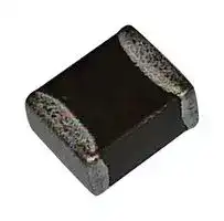
## **NTC SMD Thermistors**

## **With Nickel Barrier Termination NB 12 - NB 20**

Chip thermistors are high quality and low cost devices especially developed for surface mounting applications. They are widely used for temperature compensation but can also achieve temperature control of printed circuits.

A nickel barrier metallization provides outstanding qualities of solderability and enables this chip to meet the requirements of the most severe soldering processes.

|**Types**<br>~~a~~|**NB 12**<br>**IEC SIZE : 0805**|**NB 20**<br>**IEC SIZE : 1206**|
|---|---|---|
|**DIMENSIONS:**<br>**millimeters (inches)**<br>~~a~~|2 (.079)±0.3 (.012)<br>1.25 (.049)<br>±0.2 (.008)<br>0.5 (.020)<br>... 1.3 (.051)<br>0.2 (.008) min<br>0.2 (.008) min|3.2 (.126)±0.4 (.016)<br>0.2 (.008) min<br>0.2 (.008) min<br>1.6 (.063)<br>±0.25 (.010)<br>0.5 (.020)<br>... 1.5 (.059)|
|Terminations<br>~~———~~|Nickel Barrier||
|Marking<br>~~———~~|On packaging only||
|Climatic category<br>~~———~~<br>~~———~~|40/125/56||
|Operating temperature<br>~~———~~<br>~~———~~|-55°C to +150°C||
|Tolerance on Rn (25°C)<br>~~———~~<br>~~———~~|±5%, ±10%, ±20%||
|Maximum dissipation at 25°C<br>~~———~~<br>~~———~~|0.12 W|0.24 W|
|Thermal dissipation factor<br>~~———~~<br>~~ee~~|2 mW/°C|4 mW/°C|
|Thermal time constant<br>~~———~~<br>~~ee~~|5 s|7s|


## **APPLICATIONS**

- LCD compensation

- Battery packs

- Mobile phones

- CD players

- Heating systems

- Air-conditioning systems

- Temperature control of Switch Mode Power Supplies

- Compensation of pressure sensors

- Protection of power transistors in various electronic circuits

## **HOW TO ORDER**

**==> picture [483 x 149] intentionally omitted <==**

**----- Start of picture text -----**<br>
NB 20 K 0 0103 M BA<br>Ty Type Material Code | Resistance ar Tolerance | Suffix: Packaging |<br>K 10,000 Ω M (±20%) – –: Bulk<br>(See tables page 13) J (±5%) BA: Plastic tape<br>K (±10%) (180mm diam. reel)<br>BE: Plastic tape (1/2 reel)<br>BC: Plastic tape<br>(330mm diam. reel)<br>BB: Cardboard tape<br>(180mm diam. reel)<br>BF: Cardboard tape (1/2 reel)<br>BD: Cardboard tape<br>(330mm diam. reel)<br>**----- End of picture text -----**<br>


12

**With Nickel Barrier Termination NB 12 – NB 20**

## **NTC SMD Thermistors**

## **TABLE OF VALUES**

**==> picture [252 x 594] intentionally omitted <==**

**----- Start of picture text -----**<br>
NB 12<br>IEC SIZE : 0805<br>Rn at 25°C Material B (K) � at 25°C<br>Types<br>( Ω ) Code ( � B/B            (1) ± 5%(2) ± 3%) (%/°C)<br>NB 12 KC 0 180 18<br>NB 12 KC 0 220 22<br>NB 12 KC 0 270 27<br>NB 12 KC 0 330 33<br>NB 12 KC 0 390 39 KC 3470 ± 5% – 3.9<br>NB 12 KC 0 470  47<br>NB 12 KC 0 560  56<br>NB 12 KC 0 680  68<br>NB 12 KC 0 820  82<br>NB 12 KC 0 101  100<br>NB 12 MC 0 121  120<br>NB 12 MC 0 151  150<br>NB 12 MC 0 181  180<br>NB 12 MC 0 221  220<br>NB 12 MC 0 271  270<br>NB 12 MC 0 331  330<br>NB 12 MC 0 391  390<br>NB 12 MC 0 471  470<br>NB 12 MC 0 561 560 MC 3910 ± 3% – 4.4<br>NB 12 MC 0 681 680<br>NB 12 MC 0 821 820<br>NB 12 MC 0 102 1,000<br>NB 12 MC 0 122 1,200<br>NB 12 MC 0 152 1,500<br>NB 12 MC 0 182 1,800<br>NB 12 MC 0 222 2,200<br>NB 12 MC 0 272 2,700<br>NB 12 MC 0 332 3,300<br>NB 12 J 0 0332 3,300<br>NB 12 J 0 0392 3,900 J 3480 ± 3% – 3.9<br>NB 12 J 0 0472 4,700<br>NB 12 J 0 0562 5,600<br>NB 12 K 0 0682 6,800<br>NB 12 K 0 0822 8,200 K  3630 ± 3% – 4.0<br>NB 12 K 0 0103  10,000<br>NB 12 L 0 0123  12,000 L 3790 ± 3% – 4.2<br>NB 12 L 0 0153 15,000<br>NB 12 M 0 0183 18,000<br>NB 12 M 0 0223  22,000  M  3950 ± 3% – 4.4<br>NB 12 M 0 0273  27,000<br>NB 12 M 0 0333  33,000<br>NB 12 N 0 0393  39,000<br>NB 12 N 0 0473  47,000 N  4080 ± 3% – 4.6<br>NB 12 N 0 0563  56,000<br>NB 12 L 2 0683  68,000 L2 3805 ± 3% – 4.1<br>NB 12 N 5 0683 68,000 N5 4160 ± 3% – 4.7<br>NB 12 N 5 0823  82,000<br>NB 12 P 0 0104  100,000 P 4220 ± 3% – 4.7<br>NB 12 SC 0104  100,000 SC 4500 ± 3% – 4.8<br>NB 12 P 0 0124 120,000<br>NB 12 P 0 0154  150,000 P  4220 ± 3%  – 4.7<br>NB 12 P 0 0184  180,000<br>NB 12 Q 0 0224 220,000 Q 4300 ± 3% – 4.7<br>NB 12 Q 0 0274 270,000<br>NB 12 R 0 0105 1,000,000 R 4400 ± 3% – 4.8<br>**----- End of picture text -----**<br>


**==> picture [253 x 367] intentionally omitted <==**

**----- Start of picture text -----**<br>
NB 20<br>IEC SIZE : 1206<br>Rn at 25°C Material B (K) � at 25°C<br>Types ( Ω ) Code ( � B/B            (1) ± 5%(2) ± 3%) (%/°C)<br>NB 20 MC 0 221 220 MC 3910 ± 3% – 4.4<br>NB 20 MC 0 102 1,000 MC 3910 ± 3% – 4.4<br>NB 20 J 0 0472 4,700<br>NB 20 J 0 0562 5,600 J 3480 ± 3% – 3.9<br>NB 20 J 0 0682 6,800<br>NB 20 J 5 0822  8,200 J5 3480 ± 3% – 3.9<br>NB 20 K 0 0103 10,000 K 3630 ± 3% – 4.0<br>NB 20 K 0 0123 12,000<br>NB 20 L 0 0153 15,000<br>NB 20 L 0 0183 18,000 L 3790 ± 3% – 4.2<br>NB 20 L 0 0223 22,000<br>NB 20 M 0 0273 27,000<br>NB 20 M 0 0333 33,000 M 3950 ± 3% – 4.4<br>NB 20 M 0 0393 39,000<br>NB 20 M 0 0473 47,000<br>NB 20 N 0 0563 56,000<br>NB 20 N 0 0683 68,000 N 4080 ± 3% – 4.6<br>NB 20 N 0 0823 82,000<br>NB 20 N 5 0104 100,000 N5 4160 ± 3% – 4.7<br>NB 20 P 0 0124 120,000<br>NB 20 P 0 0154 150,000<br>NB 20 P 0 0184  180,000 P  4220 ± 3% – 4.7<br>NB 20 P 0 0224 220,000<br>NB 20 Q 0 0274 270,000<br>NB 20 Q 0 0334 330,000<br>NB 20 Q 0 0394 390,000 Q 4300 ± 3% – 4.7<br>NB 20 Q 0 0474 470,000<br>NB 20 Q 0 0564 560,000<br>NB 20 R 0 0684 680,000<br>NB 20 R 0 0824 820,000 R 4400 ± 3% – 4.8<br>NB 20 R 0 0105 1,000,000<br>**----- End of picture text -----**<br>


13

## **Packaging for Automatic Insertion**

## **NTC Chip Thermistors / NC/NB Series**

## **AUTOMATIC INSERTION**

**==> picture [497 x 112] intentionally omitted <==**

**----- Start of picture text -----**<br>
Cover Tape Hole 1 (.039) +0.2 (.008)-0<br>Max<br>Super 8 Plastic Tape Packaging: 3° A1<br>The mechanical and dimensional reel characteristics are in<br>5.5 (.217) B0 B1<br>accordance with the IEC publication 286-3. ±0.2 (.008) F W<br>Max<br>3° D0 P2<br>E<br>30µ ± 5µ P0<br>T<br>K Max3° Max3° Direction ofunreeling<br>A0<br>R = 0.3 (.012) Max.<br>**----- End of picture text -----**<br>


**==> picture [517 x 356] intentionally omitted <==**

**----- Start of picture text -----**<br>
Designation Symbol Value Tolerance<br>Tape width W 8 ±0.2<br>Tape thickness T 0.4 max.<br>—— Pitch of the sprocket holes P0 4 ±0.1<br>Diameter of the sprocket holes D0 1.5 ±0.1<br>-0<br>Distance E 1.75 ±0.1<br>Distance (center to center) F 3.5 ±0.05<br>Distance (center to center) P2 2 ±0.1<br>Sizes of the       NC 12 (0805) A0 1.5 ±0.1<br>cavities B0 2.4 ±0.1<br>K 1.4 max. K ±0.1<br>(size is adjustable)<br>(K = t1 +0.2)<br>NC 20 (1206) A0 1.95 ±0.1<br>B0 3.55 ±0.1<br>K 1.5 max. K ±0.1<br>(size is adjustable)<br>(K = t1 +0.2)<br>/ a ee<br>+ 0<br>ø180 (7.09) - 2 (.079)<br>ø 12.75 (.502)  [+ 0.15 (.006)] - 0 Reel<br>Upper side<br>Bottom side<br>Reel<br>14.4 (.567) w max. +0.15 (.006)8.4 (.331)  e according toISO/DIS 3639-2 i e<br>ø 20.5 (.087)  [+ 0.5 (.020)] - 0<br> 1.5 (.059)<br>ø 62 (2.44) ±<br>Direction of  unreeling<br>**----- End of picture text -----**<br>


## **QUANTITY PER REEL**

|**Type**|**Suffix**|**Qty Per Reel**|
|---|---|---|
|NC - NB 12|BA<br>BE|4000<br>2000|
|NC 20 - NB 20|BA<br>BE|3000<br>1500|


16

## **Packaging for Automatic Insertion**

## **NTC Chip Thermistors / NC/NB Series**

## **AUTOMATIC INSERTION**

**==> picture [520 x 128] intentionally omitted <==**

**----- Start of picture text -----**<br>
10 PITCHES CUMULATIVE<br>8mm Paper Tape Packaging: P0 TOLERANCE ON TAPE<br>The mechanical and dimensional reel characteristics T D0 P2 0.20mm (0.008)<br>are in accordance with the IEC publication 286-3.<br>E1<br>BOTTOM  TOP<br>COVER COVER F W<br>TAPE TAPE B0 E2<br>G<br>T1 A0 P1<br>a5 T1 CAVITY SIZE el A CENTER LINES d e m = “L]<br>SEE NOTE 1 OF CAVITY User Direction of Feed<br>**----- End of picture text -----**<br>


**Designation Symbol Value Tolerance** ~~ee~~ TaTappe widthe thickness ~~ee~~ WT ~~ee~~ 1.1 max.8 -.0.1/+0.3 ~~es~~ Pitch of the sprocket holes P0 4 ±0.1 Diameter of the sprocket holes 1.5 D0 ±0.1 ~~ee~~ -0/+0.1 Distance E1 1.75 ±0.1 ~~a~~ Distance (center to center) ~~ee~~ F ~~ee~~ 3.5 ±0.05 Distance (center to center) P2 2 ±0.05 ~~es~~ Cover tape thickness T1 0.10 max. Distance E2 6.25 min. Distance G 0.75 min. ~~a~~ Component pitch 0805/0603 4 ±0.1 P1 0402 2 ±0.1 ~~res ce ee~~

**==> picture [174 x 109] intentionally omitted <==**

**----- Start of picture text -----**<br>
+ 0<br>ø180 (7.09) - 2 (.079)<br>ø 12.75 (.502)  [+ 0.15 (.006)] - 0<br>Reel<br>14.4 (.567) i max. +0.15 (.006)8.4 (.331)  e according toISO/DIS 3639-2<br>ø 20.5 (.087)  [+ 0.5 (.020)] - 0<br> 1.5 (.059)<br>ø 62 (2.44) ±<br>**----- End of picture text -----**<br>


**==> picture [157 x 93] intentionally omitted <==**

**----- Start of picture text -----**<br>
Reel<br>Upper side<br>Bottom side<br>| e<br>Direction of  unreeling<br>**----- End of picture text -----**<br>


## **QUANTITY PER REEL**

|**Type**|**Suffix**|**Qty Per Reel**|
|---|---|---|
|NB - NC 12<br>NB 21|BB<br>BF|4000<br>2000|
|NB 23|BB<br>BF|10000<br>5000|


17

## **Surface Mounting Guide**

## **Chip Thermistor – Application Notes**

## **STORAGE**

Good solderability is maintained for at least twelve months, provided the components are stored in their “as received” packaging at less than 40°C and 70% RH.

## **SOLDERABILITY / LEACHING**

Terminations to be well soldered after immersion in a 60/40 tin/lead solder bath at 235 ± 5°C for 2 ± 1 seconds.

Terminations will resist leaching for at least the immersion times and conditions recommendations shown below.

**==> picture [248 x 48] intentionally omitted <==**

**----- Start of picture text -----**<br>
P/N Termination Solder Solder Immersion<br>Type Tin/Lead Temp ºC Time Seconds<br>NC AgPdPt 60/40 260 ± 5 15 max<br>NB Nickel Barrier 60/40 260 ± 5 30 ± 1<br>**----- End of picture text -----**<br>


NB products are compatible with a wide range of soldering conditions consistent with good manufacturing practice for surface mount components. This includes Pb free reflow processes with peak temperatures up to 270ºC. Recommended profiles for reflow and wave soldering are shown below for reference.

NC products are recommended for lead soldering application or gluing techniques.

## **Reflow**

**==> picture [154 x 160] intentionally omitted <==**

**----- Start of picture text -----**<br>
300<br>Preheat Natural<br>Cooling<br>250<br>200<br>220ºC<br>150 to<br>250ºC<br>100<br>  50<br>    0<br>1min 1min 10 sec. max<br>(Minimize soldering time)<br>Solder Temp.<br>**----- End of picture text -----**<br>


**==> picture [239 x 102] intentionally omitted <==**

**----- Start of picture text -----**<br>
300<br>250<br>200<br>150<br>100<br>50<br>0<br>0 50 100 150 200 250 300<br>• Pre-heating: 150°C ±15°C / 60-90s Time (s)<br>• Max. Peak Gradient: 2.5°C/s<br>Temperature °C<br>**----- End of picture text -----**<br>


- Peak Temperature: 245°C ±5°C

- Time at >230°C: 40s Max.

## **Wave**

**==> picture [154 x 167] intentionally omitted <==**

**----- Start of picture text -----**<br>
300<br>Preheat<br>Natural<br>250 Cooling<br>200 T<br>150 230ºCto<br>250ºC<br>100<br>  50<br>    0<br>1 to 2 min 3 sec. max<br>(Preheat chips before soldering)<br>T/maximum 150°C<br>Solder Temp.<br>**----- End of picture text -----**<br>


- a)  The visual standards used for evaluation of solder joints will need to be modified as lead free joints are not as bright as with tin-lead pastes and the fillet may not be as large.

- b)  Resin color may darken slightly due to the increase in temperature required for the new pastes.

- c)  Lead-free solder pastes do not allow the same self alignment as lead containing systems. Standard mounting pads are acceptable, but machine set up may need to be modified.

**==> picture [167 x 98] intentionally omitted <==**

**----- Start of picture text -----**<br>
D2<br>RECOMMENDED<br>SOLDERING PAD  D1 D3<br>LAYOUT<br>D4<br>Dimensions in<br>mm (inches)<br>D5<br>**----- End of picture text -----**<br>


## **REFLOW SOLDERING**

**==> picture [249 x 100] intentionally omitted <==**

**----- Start of picture text -----**<br>
Case<br>P/N D1 D2 D3 D4 D5<br>Size<br>1.70 0.60 0.50 0.60 0.50<br>0402 NB23<br>(.067) (.024) (.020) (.024) (.020)<br>2.30 0.80 0.70 0.80 0.75<br>0603 NB21<br>(.091) (.031) (.028) (0.31) (.030)<br>3.00 1.00 1.00 1.00 1.25<br>0805 NB12<br>(.118) (.039) (.039) (.039) (.049)<br>4.00 1.00 2.00 1.00 2.50<br>1206 NB20<br>(.157) (.039) (.079) (.039) (.098)<br>**----- End of picture text -----**<br>


## **WAVE SOLDERING**

**==> picture [249 x 81] intentionally omitted <==**

**----- Start of picture text -----**<br>
Case<br>P/N D1 D2 D3 D4 D5<br>Size<br>3.10 1.20 0.70 1.20 0.75<br>0603 NB21<br>(.122) (.047) (.028) (.047) (.030)<br>4.00 1.50 1.00 1.50 1.25<br>0805 NB12<br>(.157) (.059) (.039) (.059) (.049)<br>5.00 1.50 2.00 1.50 1.60<br>1206 NB20<br>(.197) (.059) (.079) (.059) (.063)<br>**----- End of picture text -----**<br>


18
Updated at April 28, 2026
KYOCERA AVX is a globally recognized leader in the design, development, and manufacturing of advanced electronic components. For over 50 years, the company has provided innovative solutions across the automotive, industrial, medical, military, consumer electronics, and communications markets. Supported by an extensive international network of research and production facilities, KYOCERA AVX is renowned for delivering highly reliable components that meet the stringent demands of modern engineering. The manufacturer's extensive portfolio is strongly anchored in high-performance passive components, with a particular emphasis on advanced capacitive solutions. Their offering features a comprehensive selection of polymer capacitors, RF capacitors, and supercapacitors engineered for demanding power and high-frequency requirements. This core lineup is further supported by a variety of film and aluminium electrolytic capacitors, alongside precision power inductors. Beyond passive components, KYOCERA AVX excels in robust circuit protection and discrete semiconductors. Their expertise in transient voltage suppression is demonstrated by a wide array of TVS varistors and TVS diodes, complemented by temperature-sensing NTC thermistors and reliable Schottky diodes. The product ecosystem is completed by precision timing devices, including crystals and resonators, as well as specialized RF antennas, providing engineers with a versatile and dependable foundation for next-generation technology.
About Novapart
Novapart is a B2B electronic component broker specialising in stock shortages and cost reduction. We source hard-to-find parts and identify compliant alternatives across a catalogue of 410,000+ components from 500+ manufacturers.
Learn more →Stock Shortage Specialist
When a component is unavailable, discontinued or has an unacceptable lead time, we tap into our network of vetted European and Asian distributors to source what you need — without compromising on quality or traceability.
Request a quote →Compliant Alternatives
We identify pin-to-pin, electrically equivalent substitutes that meet the same certifications (RoHS, AEC-Q100, REACH) as your original specification — validated against datasheets, not just part numbers. Often at a lower cost.
BOM Analysis service →