
Image not available
Illustrative purposes only

MYWGC3R53FFW92RAE
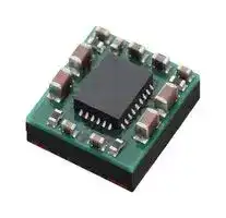
Non Isolated POL DC/DC Converter, Step Down, Module, 4 Output, 6.6 W, 3.3 V, 3.4 A
⚠️ Reference pricing provided. In case of supply shortages, we will connect you with our trusted procurement partners to ensure your project's continuity.
- Manufacturer: MURATA POWER SOLUTIONS
- Product type: DC / DC Non Isolated Board Mount Converters - Fixed Output
- SVHC: No SVHC (04-Feb-2026)
- Depth: 8.3mm
- Width: 9mm
- Height: 2.9mm
- Product Range: MonoBK MYWGC Series
- No. of Outputs: 4 Output
- Output Power Max: 6.6W
- Output Current Max: 3.4A
- Output Voltage Nom: 3.3V
- Input Voltage DC Max: 5.5V
- Input Voltage DC Min: 4.3V
- DC / DC Converter Type: Step Down, Module
- Power Supply Applications: -
- DC / DC Converter Mounting: Surface Mount Device
- DC / DC Converter Output Type: Fixed
| Delivery and price | |
|---|---|
| Units per pack | 250 |
| Price | 6.43 € |
| Current stock | 200+ |
| Lead time | 30 days |
Datasheet

**MYWGC3R53FFW92RAE**

MonoBK™, Multi output DC-DC Converter

## **PRODUCT  OVERVIEW**

**Typical unit**

## **FEATURES**

- ■Quick response to load change

- ■Ultra  small  surface mount package

   - 9.0 x 8.3 x 2.9 mm

- ■Peak efficiency of 91.0% (max.)

- ■Outstanding thermal derating performance

- ■Over Current (OCP) /Voltage (OVP) ,Under Voltage (UVP) protection and Over Temperature protection (OTP).

- ■On/Off control (Positive logic)

- ■Auto-PFM/PWM Control

- ■I2C communication function

The **MYWGC3R53FFW92RAE** is Multi output DC-DC power converters for embedded applications. The small form factor measures only 9.0 x 8.3 x 2.9 mm. Applications include powering FPGA/CPU’s, datacom/telecom systems, Distributed Bus Architectures (DBA), programmable logic and mixed voltage systems.

The converter has input voltage ranges of 4.3 to 5.5V and a multiple output voltage. Based on a fixed frequency synchronous buck converter switching topology, this high power conversion efficient PoL module features On/Off control and Power Good signal output. This product also includes under voltage lock out (UVLO), output short circuit protection, over-current protection (OCP), over-voltage protection (OVP) and over-temperature protection (OTP).

## **TYPICAL APPLICATIONS**

   - ■PCIe / server applications

   - ■FPGA and DSP

   - ■Datacom / telecom systems

   - ■Distributed bus architectures (DBA)

   - ■Programmable logic and mixed voltage systems

- ■Power Good (PG) signal

## **SIMPLIFIED APPLICATION**

**==> picture [426 x 178] intentionally omitted <==**

**----- Start of picture text -----**<br>
Vout1<br>Vin Sense1 R<br>Cout1<br>Vin Cin R R<br>Vout2<br>ON/OFF Sense2 R<br>Cout2<br>GND<br>Vout3<br>Sense3<br>R<br>PG Cout3<br>Vout4<br>SDA Sense4<br>R<br>Cout4<br>SCL<br>**----- End of picture text -----**<br>


(Typical topology is shown. Murata recommends an external input fuse.)

Export Control Code : X0863

Document No : D90DH00211

MYWGC3R53FFW92RAE A01 Page 1 of 27

**MYWGC3R53FFW92RAE**

MonoBK™, Multi output DC-DC Converter

**PERFORMANCE SPECIFICATIONS SUMMARY AND ORDERING GUIDE**

|**PERFORMANCE SPECIFICATIONSORMANCE SPECIFICATIONSRMANCE SPECIFICATIONSCE SPECIFICATIONSE SPECIFICATIONSSPECIFICATIONSPECIFICATIONSCIFICATIONSIFICATIONSCATIONSATIONSONSNSS SUMMARY AND ORDERINGMMARY AND ORDERINGORDERINGRDERINGG GUIDEIDE**|**PERFORMANCE SPECIFICATIONSORMANCE SPECIFICATIONSRMANCE SPECIFICATIONSCE SPECIFICATIONSE SPECIFICATIONSSPECIFICATIONSPECIFICATIONSCIFICATIONSIFICATIONSCATIONSATIONSONSNSS SUMMARY AND ORDERINGMMARY AND ORDERINGORDERINGRDERINGG GUIDEIDE**|**PERFORMANCE SPECIFICATIONSORMANCE SPECIFICATIONSRMANCE SPECIFICATIONSCE SPECIFICATIONSE SPECIFICATIONSSPECIFICATIONSPECIFICATIONSCIFICATIONSIFICATIONSCATIONSATIONSONSNSS SUMMARY AND ORDERINGMMARY AND ORDERINGORDERINGRDERINGG GUIDEIDE**|**PERFORMANCE SPECIFICATIONSORMANCE SPECIFICATIONSRMANCE SPECIFICATIONSCE SPECIFICATIONSE SPECIFICATIONSSPECIFICATIONSPECIFICATIONSCIFICATIONSIFICATIONSCATIONSATIONSONSNSS SUMMARY AND ORDERINGMMARY AND ORDERINGORDERINGRDERINGG GUIDEIDE**|**PERFORMANCE SPECIFICATIONSORMANCE SPECIFICATIONSRMANCE SPECIFICATIONSCE SPECIFICATIONSE SPECIFICATIONSSPECIFICATIONSPECIFICATIONSCIFICATIONSIFICATIONSCATIONSATIONSONSNSS SUMMARY AND ORDERINGMMARY AND ORDERINGORDERINGRDERINGG GUIDEIDE**|**PERFORMANCE SPECIFICATIONSORMANCE SPECIFICATIONSRMANCE SPECIFICATIONSCE SPECIFICATIONSE SPECIFICATIONSSPECIFICATIONSPECIFICATIONSCIFICATIONSIFICATIONSCATIONSATIONSONSNSS SUMMARY AND ORDERINGMMARY AND ORDERINGORDERINGRDERINGG GUIDEIDE**|**PERFORMANCE SPECIFICATIONSORMANCE SPECIFICATIONSRMANCE SPECIFICATIONSCE SPECIFICATIONSE SPECIFICATIONSSPECIFICATIONSPECIFICATIONSCIFICATIONSIFICATIONSCATIONSATIONSONSNSS SUMMARY AND ORDERINGMMARY AND ORDERINGORDERINGRDERINGG GUIDEIDE**|**PERFORMANCE SPECIFICATIONSORMANCE SPECIFICATIONSRMANCE SPECIFICATIONSCE SPECIFICATIONSE SPECIFICATIONSSPECIFICATIONSPECIFICATIONSCIFICATIONSIFICATIONSCATIONSATIONSONSNSS SUMMARY AND ORDERINGMMARY AND ORDERINGORDERINGRDERINGG GUIDEIDE**|**PERFORMANCE SPECIFICATIONSORMANCE SPECIFICATIONSRMANCE SPECIFICATIONSCE SPECIFICATIONSE SPECIFICATIONSSPECIFICATIONSPECIFICATIONSCIFICATIONSIFICATIONSCATIONSATIONSONSNSS SUMMARY AND ORDERINGMMARY AND ORDERINGORDERINGRDERINGG GUIDEIDE**|**PERFORMANCE SPECIFICATIONSORMANCE SPECIFICATIONSRMANCE SPECIFICATIONSCE SPECIFICATIONSE SPECIFICATIONSSPECIFICATIONSPECIFICATIONSCIFICATIONSIFICATIONSCATIONSATIONSONSNSS SUMMARY AND ORDERINGMMARY AND ORDERINGORDERINGRDERINGG GUIDEIDE**|**PERFORMANCE SPECIFICATIONSORMANCE SPECIFICATIONSRMANCE SPECIFICATIONSCE SPECIFICATIONSE SPECIFICATIONSSPECIFICATIONSPECIFICATIONSCIFICATIONSIFICATIONSCATIONSATIONSONSNSS SUMMARY AND ORDERINGMMARY AND ORDERINGORDERINGRDERINGG GUIDEIDE**|**PERFORMANCE SPECIFICATIONSORMANCE SPECIFICATIONSRMANCE SPECIFICATIONSCE SPECIFICATIONSE SPECIFICATIONSSPECIFICATIONSPECIFICATIONSCIFICATIONSIFICATIONSCATIONSATIONSONSNSS SUMMARY AND ORDERINGMMARY AND ORDERINGORDERINGRDERINGG GUIDEIDE**|**PERFORMANCE SPECIFICATIONSORMANCE SPECIFICATIONSRMANCE SPECIFICATIONSCE SPECIFICATIONSE SPECIFICATIONSSPECIFICATIONSPECIFICATIONSCIFICATIONSIFICATIONSCATIONSATIONSONSNSS SUMMARY AND ORDERINGMMARY AND ORDERINGORDERINGRDERINGG GUIDEIDE**|**PERFORMANCE SPECIFICATIONSORMANCE SPECIFICATIONSRMANCE SPECIFICATIONSCE SPECIFICATIONSE SPECIFICATIONSSPECIFICATIONSPECIFICATIONSCIFICATIONSIFICATIONSCATIONSATIONSONSNSS SUMMARY AND ORDERINGMMARY AND ORDERINGORDERINGRDERINGG GUIDEIDE**|**PERFORMANCE SPECIFICATIONSORMANCE SPECIFICATIONSRMANCE SPECIFICATIONSCE SPECIFICATIONSE SPECIFICATIONSSPECIFICATIONSPECIFICATIONSCIFICATIONSIFICATIONSCATIONSATIONSONSNSS SUMMARY AND ORDERINGMMARY AND ORDERINGORDERINGRDERINGG GUIDEIDE**|
|---|---|---|---|---|---|---|---|---|---|---|---|---|---|---|
|PART NUMBER<br>~~eee~~|OUTPUT<br>~~eee~~|||||||INPUT<br>~~eee~~||||Efficiency<br>[%]<br>~~eee~~|ON/OFF<br>~~eee~~|Package<br>[mm]<br>~~eee~~|
||~~eee~~|Vout<br>[V]<br>~~eee~~|Iout (max.)<br>[A]<br>~~eee~~|Power<br>[W]<br>~~eee~~|R/N (typ.)<br>[% of Vout]<br>~~eee~~|Regulation(typ.)<br>~~eee~~||Vin (typ.)<br>[V]<br>~~eee~~|Range<br>[V]<br>~~eee~~|Iin no load<br>[mA]<br>~~eee~~|Iin full<br>load<br>[A]<br>~~eee~~||||
|||||||Line [%] <br>~~eee~~|Load [%]<br>~~eee~~||||||||
|MYWGC3R53FFW92RAE<br>~~eee~~<br>~~Pease~~|Vout1<br>~~eee~~<br>~~Pease~~|1.2<br>~~eee~~<br>~~Pease~~|2.5<br>~~eee~~<br>~~Pease~~|3.0<br>~~eee~~<br>~~Pease~~|1<br>~~eee~~<br>~~Pease~~|±0.5<br>~~eee~~<br>~~Pease~~|±0.5<br>~~eee~~<br>|5<br>~~eee~~<br><br>~~IL~~|4.3 - 5.5<br>~~eee~~<br>~~TTT~~<br>~~IL~~|60<br>~~eee~~<br>~~TTT~~<br>~~IL~~|3.45<br>~~eee~~<br>~~TTT~~<br>~~IL~~|88.2<br>~~eee~~<br>~~TTT~~<br>~~IL~~|Yes<br>(Positive)<br>~~eee~~<br>~~TTT~~|9.0 x 8.3 x 2.9<br>~~eee~~<br>~~TTT~~|
||Vout2<br>~~eee~~<br>~~Pease~~|1.8<br>~~eee~~<br>~~Pease~~|1.0<br>~~eee~~<br>~~Pease~~|1.8<br>~~eee~~<br>~~Pease~~|1<br>~~eee~~<br>~~Pease~~|±0.5<br>~~eee~~<br>~~Pease~~|±0.5<br>~~eee~~<br>||||||||
||Vout3<br>~~Pease~~|3.3<br>~~Pease~~|2.0<br>~~Pease~~|6.6<br>~~Pease~~|1<br>~~Pease~~|±0.5<br>~~Pease~~|±0.5<br>||||||||
||Vout4<br>~~Pease~~|2.5<br>~~Pease~~|1.5<br>~~Pease~~|3.75<br>~~Pease~~|1<br>~~Pease~~|±0.5<br>~~Pease~~|±0.5<br>||||||||
|MYWGC3R53FFW92RA1<br>~~Pease~~|Vout1<br>~~Pease~~<br>~~SSeS~~|1.2<br>~~Pease~~<br>~~SSeS~~|2.5<br>~~Pease~~<br>~~SSeS~~|3.0<br>~~Pease~~<br>~~SSeS~~|1<br>~~Pease~~<br>~~SSeS~~|±0.5<br>~~Pease~~<br>~~SSeS~~|±0.5<br><br>~~SSeS~~|5<br> <br>~~SSeS~~<br>~~IL~~|4.3 - 5.5<br> ~~TTT~~<br>~~SSeS~~<br>~~IL~~|60<br>~~TTT~~<br>~~SSeS~~<br>~~IL~~|3.45<br>~~TTT~~<br>~~SSeS~~<br>~~IL~~|88.2<br>~~TTT~~<br>~~SSeS~~<br>~~IL~~|Yes<br>(Positive)<br>~~TTT~~<br>~~SSeS~~|9.0 x 8.3 x 2.9<br>~~TTT~~<br>~~SSeS~~|
||Vout2<br>~~Pease~~<br>~~SSeS~~|1.8<br>~~Pease~~<br>~~SSeS~~|1.0<br>~~Pease~~<br>~~SSeS~~|1.8<br>~~Pease~~<br>~~SSeS~~|1<br>~~Pease~~<br>~~SSeS~~|±0.5<br>~~Pease~~<br>~~SSeS~~|±0.5<br><br>~~SSeS~~||||||||
||Vout3<br>~~Pease~~<br>~~SSeS~~|3.3<br>~~Pease~~<br>~~SSeS~~|2.0<br>~~Pease~~<br>~~SSeS~~|6.6<br>~~Pease~~<br>~~SSeS~~|1<br>~~Pease~~<br>~~SSeS~~|±0.5<br>~~Pease~~<br>~~SSeS~~|±0.5<br><br>~~SSeS~~||||||||
||Vout4<br>~~Pease~~<br>~~SSeS~~|2.5<br>~~Pease~~<br>~~SSeS~~|1.5<br>~~Pease~~<br>~~SSeS~~|3.75<br>~~Pease~~<br>~~SSeS~~|1<br>~~Pease~~<br>~~SSeS~~|±0.5<br>~~Pease ~~<br>~~SSeS~~|±0.5<br> <br>~~SSeS~~||||||||


3. Use adequate ground plane and copper thickness adjacent to the converter.

**==> picture [472 x 127] intentionally omitted <==**

**----- Start of picture text -----**<br>
PART NUMBER STRUCTURE<br>MY WGC 3R5 3F F W 9 2 R A E<br>Murata Product Packaging Code<br>Maximum Output Current Dimension L E: Standard Quantity<br>Series Name 3F: 3.4A F: 9 ≦ D < 10 Tape and Reel 1: Small Quantity<br>Input Voltage Range<br>F: 4.3-5.5V<br>Maximum Output Voltage Terminal and<br>3R5: 3.5V Output Number Height Internal Code<br>2 ≦ T < 3<br>W: Side, 4 Outputs<br>**----- End of picture text -----**<br>


## **Product Marking**

Because of the small size of the product, the product marking contains a character-reduced code to indicate the model number and manufacturing date code. Not all items on the marking are always used. Please note that the marking differs from the product photograph. Here is the layout of the marking .

|**Part Number**|**Product Code**|
|---|---|
|MYWGC3R53FFW92RAE|AE|
|MYWGC3R53FFW92RA1|AE|


## **Layout**

## **Codes (reference)**

Internal Manufacturing code AE Product code (Please see product code table beside.)

**==> picture [8 x 15] intentionally omitted <==**

**----- Start of picture text -----**<br>
A E<br>**----- End of picture text -----**<br>


Export Control Code : X0863

Document No : D90DH00211

MYWGC3R53FFW92RAE A01 Page 2 of 27

**MYWGC3R53FFW92RAE**

## MonoBK™, Multi output DC-DC Converter

## **FUNCTIONAL SPECIFICATIONS OF MYWGC3R53FFW92RAE (Note 1)**

|**ABSOLUTE MAXIMUM RATINGS**|**Conditions**|**Minimum**|**Typical**|**Maximum**|**Units**|
|---|---|---|---|---|---|
|Vin,SCL,SDA<br>~~a~~|~~a~~|-0.3<br>~~a~~|-<br>~~a~~|6.0<br>~~a~~|V<br>~~a~~|
|ON/OFF,PG<br>~~eG~~|~~eG~~|-0.3<br>~~eG~~|-<br>~~eG~~|Vin<br>~~eG~~|V<br>~~eG~~|
|Vout1 to 4,Sense1 to 4<br>~~eG~~<br>~~GG~~|~~eG~~<br>~~GG~~|-0.3<br>~~eG~~<br>~~GG~~|-<br>~~eG~~<br>~~GG~~|3.55<br>~~eG~~<br>~~GG~~|V<br>~~eG~~<br>~~GG~~|
|Iout1<br>~~GG~~<br>~~DG~~|(Note 2)<br>~~GG~~<br>~~DG~~|-<br>~~GG~~<br>~~DG~~|-<br>~~GG~~<br>~~DG~~|2.5<br>~~GG~~<br>~~DG~~|A<br>~~GG~~<br>~~DG~~|
|Iout2<br>~~DG~~<br>~~a~~|(Note 2)<br>~~DG~~|-<br>~~DG~~|-<br>~~DG~~|1.0<br>~~DG~~|A<br>~~DG~~|
|Iout3<br>~~a~~<br>~~GG~~|(Note 2)<br>~~GG~~|-<br>~~GG~~|-<br>~~GG~~|2.0<br>~~GG~~|A<br>~~GG~~|
|Iout4<br>~~GG~~<br>~~GG~~|(Note 2)<br>~~GG~~<br>~~GG~~|-<br>~~GG~~<br>~~GG~~|-<br>~~GG~~<br>~~GG~~|1.5<br>~~GG~~<br>~~GG~~|A<br>~~GG~~<br>~~GG~~|
|Storage Temperature Range<br>~~GG~~<br>~~OO~~|Vin = Zero(nopower)<br>~~GG~~<br>~~OO~~|-40<br>~~GG~~<br>~~OO~~|-<br>~~GG~~<br>~~OO~~|125<br>~~GG~~<br>~~OO~~|degC<br>~~GG~~<br>~~OO~~|
|Soldering/ Reflow Peak Temperature<br>~~OO~~<br>~~GG~~<br>~~OO~~|(Note 22)<br>~~OO~~<br>~~GG~~<br>~~OO~~|-<br>~~OO~~<br>~~GG~~|-<br>~~OO~~<br>~~GG~~|260<br>~~OO~~<br>~~GG~~|degC<br>~~OO~~<br>~~GG~~|
|Maximum Number of Reflows Allowed<br>~~GG~~<br>~~OO~~|(Note 22)<br>~~GG~~<br>~~OO~~|~~GG~~|~~GG~~|2<br>~~GG~~|~~GG~~|
|Absolute maximums are stress ratings. Exposure of devices to greater than any of these conditions may adversely affect long-term reliability. Proper operation under conditions other than<br>those listed in the Performance/Functional Specifications Table is not implied or recommended.<br>~~OO~~||||||
|**INPUT**<br>~~OO~~|**Conditions**<br>~~OO~~|**Minimum**|**Typical**|**Maximum**|**Units**|
|OperatingVoltage Range<br>~~GG~~|~~GG~~|4.3<br>~~GG~~|5<br>~~GG~~|5.5<br>~~GG~~|V<br>~~GG~~|
|Start-upThreshold<br>~~GG~~<br>~~GG~~|Risinginput voltage<br>~~GG~~<br>~~GG~~|-<br>~~GG~~<br>~~GG~~|2.5<br>~~GG~~<br>~~GG~~|-<br>~~GG~~<br>~~GG~~|V<br>~~GG~~<br>~~GG~~|
|Under Voltage Shutdown<br>~~GG~~<br>~~OG~~|(Note 12)<br>~~GG~~<br>~~OG~~|-<br>~~GG~~<br>~~OG~~|2.2<br>~~GG~~<br>~~OG~~|-<br>~~GG~~<br>~~OG~~|V<br>~~GG~~<br>~~OG~~|
|Internal Filter Type<br>~~OG~~<br>~~a~~|~~OG~~<br>~~G~~|~~OG~~<br>~~G~~|Capacitive<br>~~OG~~|~~OG~~|~~OG~~|
|Input Current<br>~~a~~<br>~~G~~<br>~~PT~~||||||
|Full Load Condition<br>~~PT~~<br>~~OO~~|Vin=typ.<br>~~PT~~<br>~~OO~~|-<br>~~PT~~<br>~~OO~~|3.45<br>~~PT~~<br>~~OO~~|-<br>~~PT~~<br>~~OO~~|A<br>~~PT~~<br>~~OO~~|
|Low Line Condition<br>~~OO~~<br>~~GG~~|Vin=min.<br>~~OO~~<br>~~GG~~|-<br>~~OO~~<br>~~GG~~|3.98<br>~~OO~~<br>~~GG~~|-<br>~~OO~~<br>~~GG~~|A<br>~~OO~~<br>~~GG~~|
|No Load Current Condition<br>~~GG~~<br>~~QQ~~|Iout1 to 4=0A,unit=ON<br>~~GG~~<br>~~QQ~~|-<br>~~GG~~<br>~~QQ~~|0.7<br>~~GG~~<br>~~QQ~~|-<br>~~GG~~<br>~~QQ~~|mA<br>~~GG~~<br>~~QQ~~|
|**GENERAL and SAFETY**<br>~~QQ~~|**Conditions**<br>~~QQ~~|**Minimum**<br>~~QQ~~|**Typical**<br>~~QQ~~|**Maximum**<br>~~QQ~~|**Units**<br>~~QQ~~|
|Efficiency<br>~~a~~|Vin=5.0V,Iout1 to 4=max.|-|88.2|-|%|
|Control Mode<br>~~a~~||Auto-PFM/PWM||||
|Calculated MTBF (Note 3)|Ta=40degC, Vin=typ., Vout1 to 4=typ., Iout1 to 4=50%|-|5.5x10⁶|-|hours|
|**DYNAMIC CHARACTERISTICS**|**Conditions**|**Minimum**|**Typical**|**Maximum**|**Units**|
|Fixed SwitchingFrequency<br>~~a~~|Under PWM control|-|1650|-|kHz|
|StartupTime(Vin ON)<br>~~a~~<br>~~GO~~|Vout1 to 4=typ.(Vin=ON to 90% of Vout), (Note 21)<br>~~GO~~|Same as Remote ON for reference<br>~~GO~~|||ms<br>~~GO~~|
|StartupTime(Enable ON)<br>~~GO~~<br>~~a~~|Vout1 to 4=typ.(Remote=ON to 90% of Vout)<br>~~GO~~<br>~~OG~~|See the waveform for reference<br>~~GO~~<br>~~OG~~|||ms<br>~~GO~~<br>~~OG~~|
|Dynamic Load Peak Deviation<br>~~GG~~|Same as above(Note 15),Slew Rate=1.0A/us<br>~~GG~~|-<br>~~GG~~|±3<br>~~GG~~|-<br>~~GG~~|% of Vout<br>~~GG~~|
|**FUNCTIONS**<br>~~GG~~|**Conditions**<br>~~GG~~|**Minimum**<br>~~GG~~|**Typical**<br>~~GG~~|**Maximum**<br>~~GG~~|**Units**<br>~~GG~~|
|Remote On/Off Control(Note 4)<br>~~P|~~||||||
|Logic<br>~~PT~~||||||
|ON State Range<br>~~PT~~<br>~~OG~~|~~PT~~<br>~~OG~~|1.2<br>~~PT~~<br>~~OG~~|-<br>~~PT~~<br>~~OG~~|Vin<br>~~PT~~<br>~~OG~~|V<br>~~PT~~<br>~~OG~~|
|OFF Stage Range<br>~~OG~~<br>~~CG~~|~~OG~~<br>~~CG~~|-0.3<br>~~OG~~<br>~~CG~~|-<br>~~OG~~<br>~~CG~~|0.6<br>~~OG~~<br>~~CG~~|V<br>~~OG~~<br>~~CG~~|
|Power-Good Output<br>~~PT~~||||||
|Power-Good RisingThreshold<br>~~PT~~<br>~~OG~~|Noprotect<br>~~PT~~<br>~~OG~~|-<br>~~PT~~<br>~~OG~~|90<br>~~PT~~<br>~~OG~~|-<br>~~PT~~<br>~~OG~~|% of Vout<br>~~PT~~<br>~~OG~~|
|Power-Good FallingThreshold<br>~~OG~~<br>~~GG~~|Noprotect<br>~~OG~~<br>~~GG~~|-<br>~~OG~~<br>~~GG~~|80<br>~~OG~~<br>~~GG~~|-<br>~~OG~~<br>~~GG~~|% of Vout<br>~~OG~~<br>~~GG~~|
|**MECHANICAL(Common)**|**Conditions**|**Minimum**|**Typical**|**Maximum**|**Units**|
|Mechanical Dimension<br>~~a~~|L x W x H(Note 19)<br>~~a~~|9.0(typ.)x 8.3(typ.)x 3.0(max.)<br>~~a~~<br>~~O~~|||mm<br>~~a~~|
|Weight<br>~~a~~|~~a~~|-<br>~~a~~<br>~~O~~|0.65<br>~~a~~|-<br>~~a~~|grams<br>~~a~~|
|**ENVIRONMENTAL(Common)**<br>~~a~~|**Conditions**<br>~~a~~|**Minimum**<br>~~a~~<br>~~O~~|**Typical**<br>~~a~~|**Maximum**<br>~~a~~|**Units**<br>~~a~~|
|Operating Ambient Temperature Range<br>~~CO~~|With Derating (Notes 2,7)<br>~~CO~~|-40<br>~~CO~~|-<br>~~CO~~|105<br>~~CO~~|degC<br>~~CO~~|
|OperatingCase Temperature Range of TopMounted IC|Primarycondition,With Derating (Note 2)|-|-|110|degC|
|Operating Junction Temperature Range of Top Mounted<br>IC|With Derating (Note 2)|-40|-|120|degC|
|Thermal Characterization Parameter of TopMounted IC<br>~~a~~|Case tojunction of mounted IC on surface(Note 16)<br>~~CO~~|-<br>~~CO~~|5|-|degC/W|
|Storage Temperature Range<br>~~a~~<br>~~a~~|Vin=Zero(nopower)<br>~~CO~~<br>~~CO~~|-40<br>~~CO~~<br>~~CO~~|-|125|degC|
|Thermal Protection/Shutdown<br>~~OO~~|Measured in module(Note 9)<br>~~OO~~|-<br>~~OO~~|150<br>~~OO~~|-<br>~~OO~~|degC<br>~~OO~~|
|Thermal Protection/Shutdown(Recovery)<br>~~OO~~<br>~~a~~|Measured in module(Notes 9,14)<br>~~OO~~<br>~~CO~~|-<br>~~OO~~<br>~~CO~~|130<br>~~OO~~|-<br>~~OO~~|degC<br>~~OO~~|
|Moisture SensitivityLevel<br>~~a~~<br>~~a~~|~~CO~~<br>~~CO~~|3<br>~~CO~~<br>~~CO~~|||~~CO~~|
|**ENVIRONMENTAL VALIDATION TESTING(For Reference)**||||||
|**Test**|**Conditions**|||||
|Temperature Cycling<br>~~a~~|Ta=-40degC/30min <=> +125degC/30min,300cycles|||||


Export Control Code : X0863 Document No : D90DH00211

MYWGC3R53FFW92RAE A01 Page 3 of 27

**MYWGC3R53FFW92RAE**

## MonoBK™, Multi output DC-DC Converter

## **FUNCTIONAL SPECIFICATIONS OF MYWGC3R53FFW92RAE (Note 1)**

|**OUTPUT**|**Conditions**|**Minimum**|**Typical**|**Maximum**|**Units**|
|---|---|---|---|---|---|
|Total Output Power<br>~~CD~~|See Derating<br>~~CD~~|0<br>~~CD~~|-<br>~~CD~~|15.2<br>~~CD~~|W<br>~~CD~~|
|Voltage<br>~~CD~~<br>~~fT~~||||||
|Output Voltage Vout1<br>~~fT~~<br>~~GG~~|(Note 10)<br>~~fT~~<br>~~GG~~|-<br>~~fT~~<br>~~GG~~|1.2<br>~~fT~~<br>~~GG~~|-<br>~~fT~~<br>~~GG~~|V<br>~~fT~~<br>~~GG~~|
|Output Voltage Vout2<br>~~GG~~<br>~~GGG~~|(Note 10)<br>~~GG~~<br>~~GGG~~|-<br>~~GG~~<br>~~GGG~~|1.8<br>~~GG~~<br>~~GGG~~|-<br>~~GG~~<br>~~GGG~~|V<br>~~GG~~<br>~~GGG~~|
|Output Voltage Vout3<br>~~GGG~~<br>~~GO~~|(Note 10)<br>~~GGG~~<br>~~GO~~|-<br>~~GGG~~<br>~~GO~~|3.3<br>~~GGG~~<br>~~GO~~|-<br>~~GGG~~<br>~~GO~~|V<br>~~GGG~~<br>~~GO~~|
|Output Voltage Vout4<br>~~GO~~<br>~~GO~~|(Note 10)<br>~~GO~~<br>~~GO~~|-<br>~~GO~~<br>~~GO~~|2.5<br>~~GO~~<br>~~GO~~|-<br>~~GO~~<br>~~GO~~|V<br>~~GO~~<br>~~GO~~|
|Over Voltage Protection Threshold<br>~~GO~~<br>~~GGG~~|(Note 13)<br>~~GO~~<br>~~GGG~~|-<br>~~GO~~<br>~~GGG~~|120<br>~~GO~~<br>~~GGG~~|-<br>~~GO~~<br>~~GGG~~|% of Vout<br>~~GO~~<br>~~GGG~~|
|Over Voltage Protection RecoveryThreshold<br>~~GGG~~<br>~~FF~~|~~GGG~~<br>~~FF~~|-<br>~~GGG~~<br>~~FF~~|110<br>~~GGG~~<br>~~FF~~|-<br>~~GGG~~<br>~~FF~~|% of Vout<br>~~GGG~~<br>~~FF~~|
|Current<br>~~FF~~<br>~~PT~~||||||
|Output Current Range at Vout1<br>~~PT~~<br>~~GG~~|(Note 2)<br>~~PT~~<br>~~GG~~|0<br>~~PT~~<br>~~GG~~|-<br>~~PT~~<br>~~GG~~|2.5<br>~~PT~~<br>~~GG~~|A<br>~~PT~~<br>~~GG~~|
|Current Limit Inception at Vout1<br>~~GG~~<br>~~FO~~|After warm-up<br>~~GG~~<br>~~FO~~|-<br>~~GG~~<br>~~FO~~|5.5<br>~~GG~~<br>~~FO~~|-<br>~~GG~~<br>~~FO~~|A<br>~~GG~~<br>~~FO~~|
|Output Current Range at Vout2<br>~~FO~~<br>~~GG~~|(Note 2)<br>~~FO~~<br>~~GG~~|0<br>~~FO~~<br>~~GG~~|-<br>~~FO~~<br>~~GG~~|1.0<br>~~FO~~<br>~~GG~~|A<br>~~FO~~<br>~~GG~~|
|Current Limit Inception at Vout2<br>~~GG~~<br>~~GGG~~|After warm-up<br>~~GG~~<br>~~GGG~~|-<br>~~GG~~<br>~~GGG~~|3.0<br>~~GG~~<br>~~GGG~~|-<br>~~GG~~<br>~~GGG~~|A<br>~~GG~~<br>~~GGG~~|
|Output Current Range at Vout3<br>~~GGG~~<br>~~GG~~|(Note 2)<br>~~GGG~~<br>~~GG~~|0<br>~~GGG~~<br>~~GG~~|-<br>~~GGG~~<br>~~GG~~|2.0<br>~~GGG~~<br>~~GG~~|A<br>~~GGG~~<br>~~GG~~|
|Current Limit Inception at Vout3<br>~~GG~~<br>~~GG~~|After warm-up<br>~~GG~~<br>~~GG~~|-<br>~~GG~~<br>~~GG~~|5.5<br>~~GG~~<br>~~GG~~|-<br>~~GG~~<br>~~GG~~|A<br>~~GG~~<br>~~GG~~|
|Output Current Range at Vout4<br>~~GG~~<br>~~GGG~~|(Note 2)<br>~~GG~~<br>~~GGG~~|0<br>~~GG~~<br>~~GGG~~|~~GG~~<br>~~GGG~~|1.5<br>~~GG~~<br>~~GGG~~|A<br>~~GG~~<br>~~GGG~~|
|Current Limit Inception at Vout4<br>~~Po~~|After warm-up<br>~~Po~~|-<br>~~Po~~|3.0<br>~~Po~~|-<br>~~Po~~|A<br>~~Po~~|
|Short Circuit<br>~~Po~~<br>~~PT~~||||||
|Short Circuit Duration(remove short for recovery)<br>~~PT~~<br>~~GG~~|Output shorted toground,no damage<br>~~PT~~<br>~~GG~~|~~PT~~<br>~~GG~~|Continuous<br>~~PT~~<br>~~GG~~|~~PT~~<br>~~GG~~|~~PT~~<br>~~GG~~|
|Short Circuit Protection Method<br>~~A~~|(Note 5)<br>~~A~~|~~A~~|Hiccup<br>~~A~~|~~A~~|~~A~~|
|Pre-bias Start-up<br>~~A~~|~~A~~|The converter will start up if the external output voltage<br>is less than set Vout.<br>~~A~~|||voltage<br>~~A~~|
|Regulation(Notes 8,18)<br>~~A~~<br>~~PT~~||||||
|Line Regulation<br>~~PT~~<br>~~GG~~<br>~~ee~~|Vin=min. to max.,Iout1 to 4=20% load current to max.<br>~~PT~~<br>~~GG~~|-<br>~~PT~~<br>~~GG~~|±0.5<br>~~PT~~<br>~~GG~~|-<br>~~PT~~<br>~~GG~~|% of Vout<br>~~PT~~<br>~~GG~~|
|Load Regulation<br>~~ee~~|Iout1 to 4=20% load current to max.|-|±0.5|-|% of Vout|
|Total Output Voltage Variation<br>~~ee~~|Fixed Vin, Iout1 to 4=20% load current to max.<br>Tj of top IC=-40 to 120degC (Note 17)|-|-|±3|% of Vout|
|Ripple and Noise(20MHz bandwidth)<br>~~ee~~<br>~~GG~~|Iout1 to 4=20% load current to max.(Note 6)<br>~~GG~~|-<br>~~GG~~|1<br>~~GG~~|-<br>~~GG~~|% of Vout<br>~~GG~~|
|External Output Capacitance Range Vout1<br>~~ee~~<br>~~GG~~<br>~~GG~~|(Note 11)<br>~~GG~~<br>~~GG~~|44<br>~~GG~~<br>~~GG~~|-<br>~~GG~~<br>~~GG~~|400<br>~~GG~~<br>~~GG~~|uF<br>~~GG~~<br>~~GG~~|
|External Output Capacitance Range Vout2|(Note 11)|22|-|400|uF|
|External Output Capacitance Range Vout3<br>~~eG~~|(Note 11)<br>with a polymer aluminum electrolytic capacitor 47uF<br>~~eG~~|69<br>~~eG~~|-<br>~~eG~~|400<br>~~eG~~|uF<br>~~eG~~|
|External Output Capacitance Range Vout4<br>~~eG~~<br>~~GO~~|(Note 11)<br>~~eG~~<br>~~GO~~|22<br>~~eG~~<br>~~GO~~|-<br>~~eG~~<br>~~GO~~|400<br>~~eG~~<br>~~GO~~|uF<br>~~eG~~<br>~~GO~~|
|**I2C INTERFACE SPECIFICATIONS(Note 20)**<br>~~GO~~|**Conditions**<br>~~GO~~|**Minimum**<br>~~GO~~|**Typical**<br>~~GO~~|**Maximum**<br>~~GO~~|**Units**<br>~~GO~~|
|Input Logic High<br>~~GG~~|~~GG~~|1.4<br>~~GG~~|-<br>~~GG~~|-<br>~~GG~~|V<br>~~GG~~|
|Input Logic Low<br>~~GG~~<br>~~GGG~~|~~GG~~<br>~~GGG~~|-<br>~~GG~~<br>~~GGG~~|-<br>~~GG~~<br>~~GGG~~|0.4<br>~~GG~~<br>~~GGG~~|V<br>~~GG~~<br>~~GGG~~|
|Output Voltage Logic Low<br>~~GGG~~<br>~~GGG~~|~~GGG~~<br>~~GGG~~|-<br>~~GGG~~<br>~~GGG~~|-<br>~~GGG~~<br>~~GGG~~|0.4<br>~~GGG~~<br>~~GGG~~|V<br>~~GGG~~<br>~~GGG~~|
|SCL Clock Frequency<br>~~GG~~|~~GG~~|-<br>~~GG~~|-<br>~~GG~~|3.4<br>~~GG~~|MHz<br>~~GG~~|
|SCL High Time<br>~~GG~~<br>~~GGG~~|~~GG~~<br>~~GGG~~|60<br>~~GG~~<br>~~GGG~~|-<br>~~GG~~<br>~~GGG~~|-<br>~~GG~~<br>~~GGG~~|ns<br>~~GG~~<br>~~GGG~~|
|SCL Low Time<br>~~GGG~~<br>~~GGG~~|~~GGG~~<br>~~GGG~~|160<br>~~GGG~~<br>~~GGG~~|-<br>~~GGG~~<br>~~GGG~~|-<br>~~GGG~~<br>~~GGG~~|ns<br>~~GGG~~<br>~~GGG~~|
|Data Set-upTime<br>~~GG~~|~~GG~~|10<br>~~GG~~|-<br>~~GG~~|-<br>~~GG~~|ns<br>~~GG~~|
|Data Hold Time<br>~~GG~~|~~GG~~|-<br>~~GG~~|70<br>~~GG~~|-<br>~~GG~~|ns<br>~~GG~~|
|Set-upTime for Repeated Start<br>~~GG~~<br>~~GG~~|~~GG~~<br>~~GG~~|160<br>~~GG~~<br>~~GG~~|-<br>~~GG~~<br>~~GG~~|-<br>~~GG~~<br>~~GG~~|ns<br>~~GG~~<br>~~GG~~|
|Hold Time for Repeated Start<br>~~GG~~<br>~~GGG~~|~~GG~~<br>~~GGG~~|160<br>~~GG~~<br>~~GGG~~|-<br>~~GG~~<br>~~GGG~~|-<br>~~GG~~<br>~~GGG~~|ns<br>~~GG~~<br>~~GGG~~|
|Bus Free Time between Start and StopCondition<br>~~GO~~|~~GO~~|160<br>~~GO~~|-<br>~~GO~~|-<br>~~GO~~|ns<br>~~GO~~|
|Set-upTime for StopCondition<br>~~GO~~<br>~~GG~~|~~GO~~<br>~~GG~~|160<br>~~GO~~<br>~~GG~~|-<br>~~GO~~<br>~~GG~~|-<br>~~GO~~<br>~~GG~~|ns<br>~~GO~~<br>~~GG~~|
|SCL and SDA Rise Time<br>~~GG~~<br>~~GGG~~|~~GG~~<br>~~GGG~~|10<br>~~GG~~<br>~~GGG~~|-<br>~~GG~~<br>~~GGG~~|300<br>~~GG~~<br>~~GGG~~|ns<br>~~GG~~<br>~~GGG~~|
|SCL and SDA Fall Time<br>~~GO~~|~~GO~~|10<br>~~GO~~|-<br>~~GO~~|300<br>~~GO~~|ns<br>~~GO~~|
|Pulse Width of Suppressed Spike<br>~~GO~~<br>~~GG~~|~~GO~~<br>~~GG~~|0<br>~~GO~~<br>~~GG~~|-<br>~~GO~~<br>~~GG~~|50<br>~~GO~~<br>~~GG~~|ns<br>~~GO~~<br>~~GG~~|
|Capacitance Bus for Each Bus Line<br>~~GG~~<br>~~GG~~|~~GG~~<br>~~GG~~|-<br>~~GG~~<br>~~GG~~|-<br>~~GG~~<br>~~GG~~|400<br>~~GG~~<br>~~GG~~|pF<br>~~GG~~<br>~~GG~~|


Export Control Code : X0863

Document No : D90DH00211

MYWGC3R53FFW92RAE A01 Page 4 of 27

**MYWGC3R53FFW92RAE**

## MonoBK™, Multi output DC-DC Converter

## **Specification Notes**

(1)Specifications are typical at Ta=+25degC, Vin=typical (+5.0V), Vout1 to 4=typical (+1.2V, +1.8V,+3.3V,+2.5V), full load, external capacitors and natural convection unless otherwise indicated. Extended tests at full power must supply substantial natural airflow. This model is tested and specified with external capacitors shown in the test circuit below. Most capacitors are low ESR types. These capacitors are necessary to accommodate our test equipment and may not be required to achieve specified performance in your applications. However, Murata recommends installation of these capacitors.

(2)Note that Maximum Power Derating curves indicates an average current at typical input voltage. At higher temperatures and/or lower airflow, the DC/DC converter will tolerate brief full current outputs if the total RMS current over time does not exceed the Derating curve.

(3)Mean Time Between Failure is calculated by using the Telecordia SR-332 method, Ta=40degC, half output load, natural air convection.

(4)The On/Off Control Input should use either a switch or an open collector/open drain transistor to connect to GND. A logic gate may also be used by applying appropriate external voltages which do not exceed +Vin

(5)”Hiccup” overcurrent operation repeatedly attempts to restart the converter with a brief, full-current output. If the overcurrent condition still exists, the restart current will be removed and then tried again. This short current pulse prevents the converter from overheating and damaging the converter. Once the fault is removed, the converter immediately recovers normal operation.

(6)Output noise may be further reduced by adding an external filter. At zero output current or light load, the output may contain low frequency components which exceed the ripple specification. The output may be operated indefinitely with no load or light load.

(7)This model is able to start at Ta=-40degC.

(8)Regulation specifications describe the deviation as the line input voltage or output load current is varied from a nominal midpoint value to either extreme without no load and light load.

(9)Thermal Protection/Shutdown temperature is measured with the sensor in the converter. (10)Murata can review output specifications and output sequence under customer’s request. Please contact to Murata for details.

(11)The maximum output capacitive loads depend on the Equivalent Series Resistance (ESR) of the external output capacitors and, to a lesser extent, the distance and series impedance to the load in addition to ambient temperature. Larger capacitance will reduce output noise but may change the transient response. Newer ceramic capacitors with very low ESR may require lower capacitor values to avoid instability. Thoroughly test your capacitors in your applications. For reference, please refer to the “Output Capacitor Design Application Notes”. (12)Do not allow the input voltage to degrade lower than the input under voltage shutdown voltage at all times. Otherwise, you risk having the converter turn off. The under-voltage shutdown is not latching and will attempt to recover when the input is brought back into normal operating range.

(13)The outputs are not intended to sink appreciable reverse current. (14)When the temperature decreases below the recovery threshold, the converter will automatically restart.

(15)About di/dt condition, please refer to the table described later.

(16)The thermal resistance is reference data, and they are measured with our evaluation board as below.

50.0mm x 101.6mm x 1.6mm (4 Layers, 1oz copper each) FR-4

(17)Ensured by design. Not production tested.

(18)This product may not meet the specifications due to Auto PFM/PWM control at light output load.

(19)Some of product terminal shapes are different from the dimensional drawing because our dicing process might make the product terminal deformed. The deformation length is up to 150um.

(20)It is recommended to start to operate the I2C functions after the power-on sequence is complete.

(21)When Vin is ramped up slowly, the sequence may lag 3ms (max.) behind the setting.

(22)Recommended reflow profile is described in “Soldering Guidelines”.

Export Control Code : X0863 Document No : D90DH00211

MYWGC3R53FFW92RAE A01 Page 5 of 27

**MYWGC3R53FFW92RAE**

MonoBK™, Multi output DC-DC Converter

## **Internal Circuit Diagrams**

## **ON/OFF Using Guide**

By using ON/OFF function, the operation of this product can be disabled with supplying input voltage. Power-saving control with the sequence can be easy by using this function.

ON/OFF control logic

- ON/OFF pin(1pin) is pull-up                    : Output Voltage = ON

- ON/OFF pin(1pin) is connected to GND : Output Voltage = OFF

## **Example Circuit**

**==> picture [208 x 76] intentionally omitted <==**

**----- Start of picture text -----**<br>
Vin MYWGC3R53FFW92<br>RAE<br>100kohm(±5%)<br>ON/OFF<br>or<br>GND<br>**----- End of picture text -----**<br>


It is strongly recommended that the ON/OFF terminal should be used when turning on/off this product. The characteristics of the ON/OFF function may be affected by turning on/off input voltage. Please check product operation on your application with turning on/off input voltage.

## **Power Good Signal Using Guide**

The power good signal terminal should be pulled up to Vin. The resistance value for pulling up is recommended at 10kohm in case that the PG terminal is pulled up to Vin. This product has an open-drain circuit internally.

## ■PG = High situations

・ Input voltage is 4.3 to 5.5V and ON/OFF terminal is high.

・Each output voltage is within its voltage detection threshold (over 90% (typ.))    etc…

## ■PG=Low situations

・ ON/OFF pin is low and either output voltage is out of its voltage detection threshold(lower than 80% (typ.)).

・ During the PG rising delay time after all output are risen.

・ UVLO is activated.

・ Over current protection is activated.

・Over temperature protection is activated. etc…

## **Example Circuit**

**==> picture [203 x 66] intentionally omitted <==**

**----- Start of picture text -----**<br>
Vin MYWGC3R53FFW92<br>RAE<br>10kohm(±5%)<br>1 |<br>PG Power Good<br>——_ 7<br>Sink current4.0mA (max.) Ka Logic ControlCircuit<br>**----- End of picture text -----**<br>


Export Control Code : X0863 Document No : D90DH00211

MYWGC3R53FFW92RAE A01 Page 6 of 27

## **MYWGC3R53FFW92RAE**

## MonoBK™, Multi output DC-DC Converter

## **ON/OFF Sequence**

**==> picture [399 x 335] intentionally omitted <==**

**----- Start of picture text -----**<br>
ON/OFF enable ON/OFF disable<br>f<br>Circuit delay Start-up sequence ON state Shut-off sequence<br>—_r4k6<IWOTOr? 7 SA  aS<br>|<br>ON/OFF i | |<br>1 | H<br>I | |<br>Vout1 1 || || || !\ \| |<br>1 f \ |<br>Vout2 tf |l i | 1 iN! ||<br>1 ot | \ | I I f |<br>I 90% —----f--- I i I<br>Vout3<br>| J. | | —<br>i | | | 4 |_| ' ot |<br>i || | i 1 | NI<br>Vout4<br>i 1 I | to | 1 4 rot b Y<br>| i i i i | | t 1 oro yt<br>|<br>PG<br>|i|<br>0.5msec(typ.) I | PoE | Ppp Et<br>22msec(typ.) 2msec(typ.)<br>I oot<br>24msec(typ.) 6msec(typ.)<br>26msec(typ.) 8msec(typ.)<br>K< Ss le >| i] 1<br>30msec(typ.) 1 Io 10msec(typ.) | 10msec(typ.) 1 i<br>**----- End of picture text -----**<br>


Export Control Code : X0863

Document No : D90DH00211

MYWGC3R53FFW92RAE A01 Page 7 of 27

## **MYWGC3R53FFW92RAE**

MonoBK™, Multi output DC-DC Converter

**PERFORMANCE DATA AND OSCILLOGRAMS OF MYWGC3R53FFW92RAE**

Efficiency vs. Line Voltage and Load Current at Ta=25degC.

**==> picture [442 x 201] intentionally omitted <==**

**----- Start of picture text -----**<br>
95<br>90<br>85<br>80<br>75<br>1 10 100<br>Load rate of load current at all Vouts [%]<br>Vin=4.3V Vin=5.0V Vin=5.5V<br>ON/OFF Enable Delay (Vin=5.0V,  All Iout=max.) ON/OFF Enable Delay (Vin=5.0V,  All Iout=max.)<br>Trace1=Vout1 500mV/div, Trace2=Vout2 500mV/div, Trace3=Vout3 500mV/div Trace1=Vout1 500mV/div, Trace2=Vout2 500mV/div, Trace3=Vout3 500mV/div<br>Trace4=Vout4 500mV/div, Trace5=ON/OFF 1V/div, Trace6=PG 1V/div, 10ms/div Trace4=Vout4 500mV/div, Trace5=ON/OFF 1V/div, Trace6=PG 1V/div, 4ms/div<br>Efficiency [%]<br>**----- End of picture text -----**<br>


**==> picture [27 x 102] intentionally omitted <==**

**----- Start of picture text -----**<br>
Vout1 500mV/div<br>Vout2 500mV/div<br>Vout3 500mV/div<br>Vout4 500mV/div<br>ON/OFF 1V/div<br>PG 1V/div<br>**----- End of picture text -----**<br>


**==> picture [26 x 101] intentionally omitted <==**

**----- Start of picture text -----**<br>
Vout1 500mV/div<br>Vout2 500mV/div<br>Vout3 500mV/div<br>Vout4 500mV/div<br>ON/OFF 1V/div<br>PG 1V/div<br>**----- End of picture text -----**<br>


Output Ripple and Noise (Vin=5.0V,  All Iout=max.) Trace1=Vout1(AC) 1mV/div, Trace2=Vout2(AC) 1mV/div, Trace3=Vout3(AC) 1mV/div, Trace4=Vout4(AC) 1mV/div, 1us/div

Output Ripple and Noise (Vin=5.0V,  All Iout=no load) Trace1=Vout1(AC) 5mV/div, Trace2=Vout2(AC) 5mV/div, Trace3=Vout3(AC) 5mV/div, Trace4=Vout4(AC) 5mV/div, 20ms/div

**==> picture [266 x 91] intentionally omitted <==**

**----- Start of picture text -----**<br>
Vout1(AC) 1mV/div Vout1(AC) 5mV/div<br>Vout2(AC) 1mV/div Vout2(AC) 5mV/div<br>S SS ti —<br>Vout3(AC) 1mV/div Vout3(AC) 5mV/div<br>Vout4(AC) 1mV/div Vout4(AC) 5mV/div<br>**----- End of picture text -----**<br>


Export Control Code : X0863 Document No : D90DH00211

MYWGC3R53FFW92RAE A01 Page 8 of 27

**MYWGC3R53FFW92RAE**

## MonoBK™, Multi output DC-DC Converter

**==> picture [459 x 399] intentionally omitted <==**

**----- Start of picture text -----**<br>
PERFORMANCE DATA AND OSCILLOGRAMS OF MYWGC3R53FFW92RAE<br>Vout1 vs. Line Voltage and Load Current at Ta=25degC.  Vout2 vs. Line Voltage and Load Current at Ta=25degC.<br>1.236 1.854<br>1.224 1.836<br>1.212 1.818<br>1.2 1.8<br>1.188 1.782<br>1.176 1.764<br>1.164 1.746<br>0 0.5 1 1.5 2 2.5 0 0.2 0.4 0.6 0.8 1<br>Output current  Iout1 [A] Output current  Iout2 [A]<br>Vin=4.3V Vin=5.0V Vin=5.5V Vin=4.3V Vin=5.0V Vin=5.5V<br>Vout3 vs. Line Voltage and Load Current at Ta=25degC. Vout4 vs. Line Voltage and Load Current at Ta=25degC.<br>3.399<br>2.575<br>3.366<br>2.55<br>3.333<br>2.525<br>3.3<br>2.5<br>3.267 2.475<br>3.234 2.45<br>3.201 2.425<br>0 0.5 1 1.5 2 0 0.3 0.6 0.9 1.2 1.5<br>Output current  Iout3 [A] Output current  Iout4 [A]<br>Vin=4.3V Vin=5.0V Vin=5.5V Vin=4.3V Vin=5.0V Vin=5.5V<br>Output voltage  Vout1 [V] Output voltage  Vout2 [V]<br>Output voltage  Vout3 [V] Output voltage  Vout4 [V]<br>**----- End of picture text -----**<br>


## **Note**

(1)The load regulation data above is measured under conditions of varying output currents at other Vouts at same load rate.

Export Control Code : X0863

Document No : D90DH00211

MYWGC3R53FFW92RAE A01 Page 9 of 27

**MYWGC3R53FFW92RAE**

## MonoBK™, Multi output DC-DC Converter

## **PERFORMANCE DATA AND OSCILLOGRAMS OF MYWGC3R53FFW92RAE**

Step Load Transient Response (Vin=5.0V, Vout1=1.2V, Iout1=1.25 to 2.5A) Trace1=Vout1(AC) 10mV/div, Trace2=Iout1, 500mA/div, 20us/div

Step Load Transient Response (Vin=5.0V, Vout1=1.2V, Iout1=2.5 to 1.25A) Trace1=Vout1(AC), 10mV/div, Trace2=Iout1, 500mA/div, 20us/div —x ΔV=33mV AA eres Vout1(AC) 10mV/div _ Iout1 500mA/div

**==> picture [165 x 55] intentionally omitted <==**

**----- Start of picture text -----**<br>
Vout1(AC) 10mV/div<br>nO | -<br>y<br>ΔV=32mV<br>Iout1 500mA/div<br>**----- End of picture text -----**<br>


Step Load Transient Response (Vin=5.0V, Vout2=1.8V, Iout2=0.5 to 1.0A) Trace1=Vout2(AC), 5mV/div, Trace2=Iout2, 200mA/div, 20us/div

Step Load Transient Response (Vin=5.0V, Vout2=1.8V, Iout2=1.0 to 0.5A) Trace1=Vout2(AC), 5mV/div, Trace2=Iout2, 200mA/div, 20us/div

**==> picture [261 x 55] intentionally omitted <==**

**----- Start of picture text -----**<br>
Vout2(AC) 5mV/div - at = ΔV=14mV<br>en ee ee a etme Catal CS<br>ws herve<br>¢ oe ee<br>ΔV=14mV<br>Iout2 200mA/div<br>**----- End of picture text -----**<br>


Vout2(AC) 5mV/div _— fines

Iout2 200mA/div

Step Load Transient Response (Vin=5.0V, Vout3=3.3V, Iout3=1.0 to 2.0A) Trace1=Vout3(AC), 10mV/div, Trace2=Iout3, 500mA/div, 40us/div

**==> picture [163 x 62] intentionally omitted <==**

**----- Start of picture text -----**<br>
Vout3(AC) 10mV/div<br>mteeceNoeeee.<br>ΔV=22mV<br>Iout3 500mA/div<br>**----- End of picture text -----**<br>


Step Load Transient Response (Vin=5.0V, Vout4=2.5V, Iout4=0.75 to 1.5A) Trace1=Vout4(AC), 10mV/div, Trace2=Iout4, 200mA/div, 20us/div

**==> picture [177 x 53] intentionally omitted <==**

**----- Start of picture text -----**<br>
Vout4(AC) 10mV/div<br>es<br>ΔV=23mV ~~<br>Iout4 200mA/div<br>**----- End of picture text -----**<br>


Step Load Transient Response (Vin=5.0V, Vout3=3.3V, Iout3=2.0 to 1.0A) Trace1=Vout3(AC), 10mV/div, Trace2=Iout3, 500mA/div, 40us/div

> ΔV=23mV Vout3(AC) 10mV/div re Iout3 500mA/div 40us/div Step Load Transient Response (Vin=5.0V, Vout4=2.5V, Iout4=1.5 to 0.75A) Trace1=Vout4(AC), 10mV/div, Trace2=Iout4, 200mA/div, 20us/div Teltrontx x

> ΔV=23mV Vout4(AC) 10mV/div an ~~ [eeexy Iout4 200mA/div 20us/div Export Control Code : X0863 Document No : D90DH00211

MYWGC3R53FFW92RAE A01 Page 10 of 27

**MYWGC3R53FFW92RAE**

## MonoBK™, Multi output DC-DC Converter

## **THERMAL DERATINGS OF MYWGC3R53FFW92RAE**

**==> picture [139 x 7] intentionally omitted <==**

**----- Start of picture text -----**<br>
Maximum Current Temperature Derating at Sea Level<br>**----- End of picture text -----**<br>


**==> picture [212 x 138] intentionally omitted <==**

**----- Start of picture text -----**<br>
Position of the IC top temperature<br>Tc<br>**----- End of picture text -----**<br>


Thermal deratings are evaluated in following conditions.

- ・The product is mounted on 114.5 x 101.5 x 1.6mm (Layer1, 4: 2oz copper / Layer2, 3: 1oz copper) FR-4 board. ・No forced air flow.

Top temperature of the IC mounted on the product Tc: 110degC (max.)

## **TRANSIENT RESPONSE DATAS OF MYWGC3R53FFW92RAE**

Transient response data at various conditions are showed in following table. Test circuit condition can serve less than 3% of Vout deviation for 50% to 100% load change(1.0A/us) at room temperature.

||Vin [V]|Cout [uF]|Voltage Deviation[mV]|
|---|---|---|---|
||||50-100% Load Step (1.0A/us)|
|Vout1=1.2V|4.3|22 x 2|32|
||5.5||33|
|Vout2=1.8V|4.3|22 x 1|15|
||5.5||14|
|Vout3=3.3V|4.3|22 + 47|23|
||5.5||23|
|Vout4=2.5V|4.3|22 x 1|24|
||5.5||23|


Export Control Code : X0863

Document No : D90DH00211

MYWGC3R53FFW92RAE A01 Page 11 of 27

**MYWGC3R53FFW92RAE**

## MonoBK™, Multi output DC-DC Converter

## **MECHANICAL SPECIFICATIONS**

## **Dimension and Pin Assignment**

**==> picture [208 x 269] intentionally omitted <==**

**----- Start of picture text -----**<br>
<Top View>  <Side View><br>=== cq] df<br>Cj —a<br>a<br>ieeea<br>|_| .<br>oA ul gd,<br>8.30 (typ.)<br>(typ.)<br>9.00<br>(typ.)<br>2.90<br>**----- End of picture text -----**<br>


**==> picture [54 x 9] intentionally omitted <==**

**----- Start of picture text -----**<br>
<Side View><br>**----- End of picture text -----**<br>


**==> picture [87 x 11] intentionally omitted <==**

**----- Start of picture text -----**<br>
<Bottom View><br>**----- End of picture text -----**<br>


**==> picture [81 x 37] intentionally omitted <==**

**----- Start of picture text -----**<br>
Tolerance : ±0.15<br>Coplanarity : less than 0.12<br>[Unit : mm]<br>(without burr)<br>**----- End of picture text -----**<br>


Export Control Code : X0863 Document No : D90DH00211

MYWGC3R53FFW92RAE A01 Page 12 of 27

**MYWGC3R53FFW92RAE**

## MonoBK™, Multi output DC-DC Converter

## **Pin Function & Descriptions**

|**INPUT/OUTPUT Pins Functions & Descriptions**|**INPUT/OUTPUT Pins Functions & Descriptions**|**INPUT/OUTPUT Pins Functions & Descriptions**|
|---|---|---|
|**Pin No.**|**Name**|**Function & Description**|
|1, 4, 7, 10, 11, 14, 15,<br>20,23,24,27,28|GND|Power GND|
|2|ON/OFF|Power-on/off input. Logic input pin to start up or shut down the device. This pin should be<br>pulledhighby anexternal voltage.|
|3|PG|Power good open-drain output. This pin requires an external pull-up resistor.|
|5|SCL|I2C clock signal input.|
|6|SDA|I2C data pin.|
|8|Vout4|Vout4 output.|
|9|Sense4|Vout4 sense pin. Connect Vout4 output line directly to this pin.|
|12|Sense2|Vout2 sense pin. Connect Vout2 output line directly to this pin.|
|13|Vout2|Vout2 output.|
|16-19|Vin|Supply voltage input.|
|21|Vout1|Vout1 output.|
|22|Sense1|Vout1 sense pin. Connect Vout1 output line directly to this pin.|
|25|Vout3|Vout3 output.|
|26|Sense3|Vout3 sense pin. Connect Vout3 output line directly to this pin.|


Export Control Code : X0863 Document No : D90DH00211

MYWGC3R53FFW92RAE A01 Page 13 of 27

## **MYWGC3R53FFW92RAE**

## MonoBK™, Multi output DC-DC Converter

## **Recommended Board Land Pattern (Top View)**

**==> picture [356 x 274] intentionally omitted <==**

**----- Start of picture text -----**<br>
I: 1.3<br>1' !<br>I : 0.85 0.4<br>1! |<br>! 0.9 0.2 0.9 0.2 : 0.9 0.2 0.9<br>I [I]<br>1.3<br>I 0.9 : | !<br>1 i 0.8 !<br>I I 0.6<br>i !<br>l!<br>I i ] 0.8<br>1:<br>I 2.1 i ]<br>0.8<br>: !<br>I i l 0.8<br>0.85<br>1 0.2 i ! 0.6<br>!!<br>I i ]<br>1 0.85 '<br>I i ] 1.3<br>0.9 0.2 0.9 0.2 0.9 0.2 0.9<br>I [I]<br>!:<br>I [1] 0.4<br>I i 0.4<br>I [I]<br>1 1.3<br>_ 0.8 I Unit: mm<br>2.25 0.6 0.8 0.8 0.8 0.8 0.6 2.25<br>**----- End of picture text -----**<br>


## **Example of Pattern Layout (Top View)**

## **Picture**

**==> picture [218 x 106] intentionally omitted <==**

**----- Start of picture text -----**<br>
Vin NG GND<br>GFA ;<br>ve i<br>Vout1 Cin Vout2<br>X ‘ “4Myelylgtyy 5 a Trae Cin dy ly Villdys<br>a KAee ees -_ | ri | = Z bearf abo<br>GND GND<br>(GLAIED ag BESSS lla LA SOSpg SIDA hd<br>jiiatAbeee es 2 « | aan8 i ZigiayWeeDIN)AeAZa<br>Cout Cout Cout<br>Cout Cout Cout<br>**----- End of picture text -----**<br>


Export Control Code : X0863

Document No : D90DH00211

MYWGC3R53FFW92RAE A01 Page 14 of 27

## **MYWGC3R53FFW92RAE** muPata ~~eeses—(—istsi—<—~sSs—s—s—S~~

## MonoBK™, Multi output DC-DC Converter

## **Application Circuit & BOM list (Evaluation Board)**

**==> picture [475 x 533] intentionally omitted <==**

**----- Start of picture text -----**<br>
SCL SCL Sense1 Sense1<br>Vout1 Vout1<br>SDA SDA a)<br>+<br>C11 C12 C13 C14 R11 C15 C16 C17 C18<br>Vin-Sense GND GND<br>5 1115<br>Vin<br>Sense2 Sense2<br>Vin<br>Vout2 Vout2<br>TTT + ys, +<br>C9 C1 C2 C3~8 C21 C22 C23 C24 R21 C25 C26 C27 C28<br>GND GND<br>GND Sense3 Sense3<br>GND  Vout1 Vout3<br>GND-Sense O— | [A > re a a <<br>+<br>R1 C31 C32 C33 C34 R31 C35 C36 C37 C38<br>ON/OFF GND GND<br>: if ON/OFF TU<br>R2<br>Sense4 Sense4<br>PG Vout4 Vout4<br>O a PG | \ $y99 1 + O: O<br>| C41 C42 C43 C44 R41 C45 C46 C47 C48<br>GND GND<br>GND<br>(Thermal Pad)<br>— ————————9o<br>MYWGC3R53FFW92RAE<br>C1, C2 22uF/10V GRM21BD71A226ME44L<br>(Murata)<br>C11, C12, C21, C31, C41 22uF/6.3V GRM21BD70J226ME44L<br>(Murata)<br>C38 47uF/6.3V ECASD40J476M025K00<br>(Murata)<br>R1 1608M, Chip resistor, 100kohm<br>R2 1608M, Chip resistor, 10kohm<br>C3-9, C13-18, C22-28 No mount<br>C32-C37, C42-C48<br>R11, R21, R31, R41<br>**----- End of picture text -----**<br>


Export Control Code : X0863 Document No : D90DH00211

MYWGC3R53FFW92RAE A01 Page 15 of 27

## **MYWGC3R53FFW92RAE**

MonoBK™, Multi output DC-DC Converter

## **TAPE AND REEL INFORMATION**

## **Tape Dimension**

**==> picture [354 x 470] intentionally omitted <==**

**----- Start of picture text -----**<br>
1 I pit I ys~F TBD =<br>a | EEE ass |<br>1<br>al | | |<br>(7.25) B<br>8,750.1<br>5) Unit: mm<br>TBD<br>|<br>t+}<br>Section A-A<br>25.5± 1.0<br>A<br>2.0 ± 0.5<br>Indication<br>φ 21.0 ± 0.8 φ 13.0 ± 0.5<br>Unit: mm<br>Portion A<br>1 2<br>± ±<br>100 330<br>φ φ<br>**----- End of picture text -----**<br>


**==> picture [69 x 9] intentionally omitted <==**

**----- Start of picture text -----**<br>
Reel Dimension<br>**----- End of picture text -----**<br>


Export Control Code : X0863 Document No : D90DH00211

MYWGC3R53FFW92RAE A01 Page 16 of 27

## **MYWGC3R53FFW92RAE**

## MonoBK™, Multi output DC-DC Converter

## **TAPE SPECIFICATIONS** ~~ee~~

**==> picture [335 x 130] intentionally omitted <==**

**----- Start of picture text -----**<br>
Empty portion Empty portion Leader portion<br>(200mm  MIN) (180mm  MIN) (200mm  MIN)<br>"Module on  tape" portion<br>Indication<br>**----- End of picture text -----**<br>


**==> picture [237 x 72] intentionally omitted <==**

**----- Start of picture text -----**<br>
Circle Hole<br>-—sh 0 oF<br>O OO O O 0 OO O<br>No.1 Pin 1 Pin<br>xxxM xxx xxx M xxx Pulling Direction<br>**----- End of picture text -----**<br>


## **Notes**

1. The adhesive strength of the protective tape must be within 0.3-1.0N.

2. Each reel contains the quantities such as the table below.

3. Each reel set in moisture-proof packaging because of MSL 3.

4. No vacant pocket in “Module on tape” section.

5. The reel is labeled with Murata part number and quantity.

6. The color of reel is not specified.

|**Part Number**|**Quantity**|
|---|---|
|**MYWGC3R53FFW92RAE**|**Quantity**<br>**400**|
|**MYWGC3R53FFW92RA1**|**100**|


Export Control Code : X0863

Document No : D90DH00211

MYWGC3R53FFW92RAE A01 Page 17 of 27

**MYWGC3R53FFW92RAE**

## MonoBK™, Multi output DC-DC Converter

## **TECHNICAL NOTES**

## **Input Fuse**

Certain applications and/or safety agencies may require fuses at the inputs of power conversion components. Fuses should be also used when there is the possibility of sustained input voltage reversal which is not current limited. For greatest safety, we recommend a fast blow fuse installed in the ungrounded input supply line. The installer must observe all relevant safety standards and regulations. For safety agency approvals, install the converter in compliance with the end-user safety standard.

## **Input Under-Voltage Shutdown and Start-Up Threshold**

Under normal start-up conditions, the converter will not begin to regulate properly until the ramping-up input voltage exceeds and remains within the Inout Voltage Range (see Specifications). Once operating, the converter will not turn off until the input voltage drops below the Under-Voltage Shutdown Limit. Subsequent restart will not occur until the input voltage rises again above the Start-Up Threshold. This built-in hysteresis prevents any unstable on/off operation at a single input voltage. Users should be aware however of input sources near the Under-Voltage Shutdown whose voltage decays as input current is consumed (such as capacitor inputs), the converter shuts down and then restarts as the external capacitor recharges. Such situations could oscillate. To prevent this, make sure the operating input voltage is well above the UV Shutdown voltage at all times.

## **Recommended Output Filtering**

The converter will achieve its rated output ripple and noise with additional external capacitors. Users may install more external output capacitance to reduce the ripple even further, to improve dynamic response and to ensure the operation stability. Initially we recommend to use low-ESR ceramic (Murata GRM21 series) as described in our circuits. Mount these close to the converter. Check the operation stability with margin and measure the output ripple in your application. If necessary to meet your requested specification, please add the capacitors in parallel up to achieving your requested specification according to Output Capacitor Design Notes. Excessive capacitance can make step load recovery sluggish or possibly introduce instability. Do not exceed the maximum rated output capacitance listed in the specifications.

## **Output Noise**

The converter is tested and specified for output noise using designated external output components, circuits and layout as shown in the figures below. In the figure below, the two copper strips simulate real-world printed circuit impedances between the power supply and its load. In order to minimize circuit errors and standardize tests between units, scope measurements should be made using BNC connectors or the probe ground should not exceed one half inch and soldered directly to the test circuit.

## **Start-Up Time**

The Startup Time (see Specifications) will vary with input source impedance, external input capacitance, input voltage slew rate and final value of the input voltage as it appears at the converter.

The converter includes a soft start circuit to moderate the duty cycle of its PFM/PWM controller at power up, thereby limiting the input inrush current. The On/Off Remote Control interval from On command to Vout regulated assumes that the converter already has its input voltage stabilized above the Start-Up Threshold before the On command. The interval is measured from the On command until the output enters and remains within its specified accuracy band. The specification assumes that the output is fully loaded at maximum rated current. Similar conditions apply to the On to Vout regulated specification such as external load capacitance and soft start circuitry.

## **Recommended Input Filtering**

Users must assure that the input source has low AC impedance to provide dynamic stability and that the input supply has little or no inductive content, including long distributed wiring to a remote power supply. For best performance, we recommend installing a low-ESR capacitor immediately adjacent to the converter’s input terminals.

The capacitor should be a ceramic type such as the Murata GRM21 series and an electrolytic type such as Panasonic OS-CON series. Initial suggested capacitor values are 22 uF x 2 ceramic type, rated at twice the expected maximum input voltage. Make sure that the input terminals do not go below the under-voltage shutdown voltage at all times. More input bulk capacitance may be added in parallel (either electrolytic or tantalum) if needed.

C1= Cout conditions (described in the test circuit for each Vout) C2=OPEN Figure :Measuring Output Ripple and Noise

## **Minimum Output Loading Requirements**

This model regulates within specifications and is stable with the specified load conditions. Operation at no load might however increase output ripple and noise due to PFM control.

## **Thermal Shutdown**

To prevent many over temperature problems and damage, the converter includes thermal shutdown circuitry. If environmental conditions cause the temperature rise of the converter above the Operating Temperature Range up to the shutdown temperature, an on-board electronic temperature sensor will power down the unit. When the temperature decreases below the turn-on threshold, the converter will automatically restart.

**CAUTION:** If you operate too close to the thermal limits, the converter may shut down suddenly without warning. Be sure thoroughly to avoid unplanned thermal shutdown in your application.

Export Control Code : X0863 Document No : D90DH00211

MYWGC3R53FFW92RAE A01 Page 18 of 27

**MYWGC3R53FFW92RAE**

## MonoBK™, Multi output DC-DC Converter

## **Temperature Derating Curves**

The graph in this data sheet illustrates typical operation under a variety of conditions. The derating curve shows the maximum continuous ambient air temperature. Note that these are AVERAGE measurements.

Note that the temperatures are of the ambient airflow, not the converter itself which is obviously running at higher temperature than the outside air. Also note that very low flow rates (below about 25 LFM) are similar to “natural convection,” that is, not using fan-forced airflow. We use both thermocouples and an infrared camera system to observe thermal performance.

**CAUTION:** The graph is collected at slightly above Sea Level altitude. Be sure to reduce the derating for higher density altitude.

## **Output Current Limiting**

Current limiting inception is defined as the point at which full power falls below the rated tolerance. See the Performance/Functional Specifications. Note particularly that the output current may briefly rise above its rated value in normal operation as long as the average output power is not exceeded. This enhances reliability and continued operation of your application. If the output current is too high, the converter will enter the short circuit condition.

## **Output Short Circuit Condition**

When the converter is in current-limit mode, the output voltage will drop as the output current demand increases. Following a time-out period, the converter will restart, causing the output voltage to begin ramping up to its appropriate value. If the short-circuit condition persists, another shutdown cycle will initiate. This rapid on/off cycling is called “hiccup mode”. The hiccup cycling reduces the average output current, thereby preventing excessive internal temperatures and/or component damage. A short circuit can be tolerated indefinitely.

## **OVP Function**

This product monitors a feedback voltage to detect over voltage. When the feedback voltage becomes higher than 120% of the target voltage, the circuit operates sink-mode to decrease output voltage. If the output voltage decrease 110% of target voltage, the circuit returns normal operation.

## **Remote On/Off Control**

Please refer to the Connection Diagram on page 6 for On/Off connections. The model is enabled when the On/Off pin is pulled high with respect to GND. Positive-polarity devices are disabled when the On/Off is grounded or brought to within a low voltage (see Specifications) with respect to GND.

Dynamic control of the On/Off function should be able to sink appropriate signal current when brought low and withstand appropriate voltage when brought high. Be aware too that there is a finite time in milliseconds (see Specifications) between the time of On/Off Control activation and stable, regulated output. This time will vary slightly with output load type and current and input conditions.

## **Output Capacitive Load**

Users should consider adding capacitance to reduce switching noise and/or to handle spike current load steps. Install enough capacitance to achieve noise objectives. However excess external capacitance may cause regulation problems, degraded transient response and possible oscillation or instability.

The “hiccup” system differs from older latching short circuit systems because you do not have to power down the converter to make it restart. The system will automatically restore operation as soon as the short circuit condition is removed.

## **Output Voltage Remote Sense**

This function is capable to compensate up the voltage drop between the output and input of load. The voltage of the Vout pin must NOT be over their allowed maximum voltage if using the remote sense. The sense trace should be connected to Vout line as shortly as possible. The sense trace should be shielded by GND line or something else to reduce noise pick-up. The powerline length from the product to a sensing point should be within 10cm for output voltage stability. If the remote sense is not needed, the Sense pin should be connected to the Vout pin directly.

Export Control Code : X0863 Document No : D90DH00211

MYWGC3R53FFW92RAE A01 Page 19 of 27

**MYWGC3R53FFW92RAE**

## MonoBK™, Multi output DC-DC Converter

## **Soldering Guidelines**

Murata recommends the specifications below when installing the converter. These specifications vary depending on the solder type. Exceeding these specifications may cause damage to the product. Your production environment may differ. Therefore, please thoroughly review these guidelines with your process engineers. This product can be reflowed twice.

|**Reflow Solder Operations for surface-mountproducts**|**Reflow Solder Operations for surface-mountproducts**|
|---|---|
|For Sn/Ag/Cu based solders:||
|Preheat Temperature|Less than 1degCper second|
|Time over Liquidus|45 to 75 seconds|
|Maximum Peak Temperature|245degC<br>260|
|CoolingRate|Less than 3degCper second|
|For Sn/Pb based solders:||
|Preheat Temperature|Less than 1degCper second|
|Time over Liquidus|60 to 75 seconds|
|Maximum Peak Temperature|235degC|
|CoolingRate|Less than 3degCper second|


## **Pb-free Solder Processes**

For Pb-free solder processes, the product is qualified for MSL 3 according to IPC/JEDEC standard J-STD-020D. During reflow the product temperature must not exceed 260degC at any time.

## **Dry Pack Information**

Products intended for Pb-free reflow soldering processes are delivered in standard moisture barrier bags according to IPC/JEDEC standard J-STD-033. (Handling, packing, shipping and use of moisture/reflow sensitivity surface mount devices.) Using products in high temperature Pb-free soldering processes requires dry pack storage and handling. In case the product has been stored in an uncontrolled environment and no longer can be considered dry, the modules must be baked according to J-STD-033.

## **Recommended Lead-free Solder Reflow Profile**

**==> picture [22 x 15] intentionally omitted <==**

**----- Start of picture text -----**<br>
Peak235~ 260  Temp<br>**----- End of picture text -----**<br>


**CAUTION: Do not reflow the converter as follows, because the converter may fall from the substrate during reflowing.**

Export Control Code : X0863

Document No : D90DH00211

MYWGC3R53FFW92RAE A01 Page 20 of 27

**MYWGC3R53FFW92RAE**

## MonoBK™, Multi output DC-DC Converter

## **I2C INTERFACE**

## **I2C Serial Interface Description**

The I2C is a two-wire, bidirectional serial interface consisting of a clock line (SCL) and a data line (SDA). The lines are externally pulled to a bus voltage when they are idle. A master device is connected to the lines. Then it generates the SCL signal and device address, and arranges the communication sequence. The interface of the product is an I2C slave that can support fast mode (400kHz). The I2C interface makes it possible to monitor the product status. If the master sends the address as an 8-bit value, the 7-bit address should be followed by 0 or 1 to indicate a read operation. When the I2C is not used, SCL and SDA should be pulled high (5V) by a resistor (4.7kohm).

## **Transfer Data**

Data is transmitted in 8-bit bytes through SDA line. Each byte of data should be followed by an acknowledge (ACK) bit.

## **I2C Update Sequence**

The product requires a start condition, a valid I2C address, a register address byte and a data byte for a single data update. After receiving each byte, the product acknowledges the byte by pulling the SDA line low during the high period of a SCL pulse. A valid I2C address selects the product. The product performs an update on the falling edge of the LSB byte. Example of I2C read sequence is described below.

**CAUTION:** When the I2C is not used, SCL and SDA should be pulled high (5V) by a resistor (4.7kohm).

## **Start and Stop Conditions**

The start and stop conditions are signaled by the master device, and signify the beginning and the end of the I2C transmission. The start condition is defined as the SDA signal transition from high to low while the SCL is high. The stop condition is defined as the SDA signal transition from low to high while the SCL is high. The master then generates the SCL clocks, and transmits the device address and the Read bit on the SDA line.

## **I2C Write Example**

|||||8 bits||8 bits<br>8 bits|8 bits<br>8 bits||8 bits<br>8 bits|||||||
|---|---|---|---|---|---|---|---|---|---|---|---|---|---|---|---|
|S<br>~~| ~~||Slave Address<br> ~~[|~~||Slave Address<br>WR<br>~~tf ~~|A<br>Register Address K<br>A<br>Write Data K<br>A<br>Write Data K+1<br>A<br>Write Data K+N<br>A<br>P<br>・・・<br> ~~TT~~<br>~~Ft~~<br>~~Tt~~<br>~~Ty~~<br>~~~Lft~~<br>~~(2~~<br>~~F_~~|||||||||||
|||||||||Multi-byte write executed from current register location||||||||
|||||||||(the read-only register will be skipped)||||||||
|**I2C Read Example**|**I2C Read Example**|||||||||||||||
|||||8 bits||8 bits|||8 bits<br>8 bits|||||||
|S<br>Slave Address<br>WR<br>A<br>Register Address K<br>A<br>~~Pf~~<br>~~COU CE~~<br>~~(9~~|||||||||Sr<br>Slave Address<br>RD<br>A<br>Read Data K|NA||P||||
|||||Register address to read specified||Register address to read specified|||Read register data from current register location|||||||
|||CI]||Master to Slave||A = Acknowledge (SDA = Low)                    S = Start Condition          Sr = Repeat Start Condition|A = Acknowledge (SDA = Low)                    S = Start Condition          Sr = Repeat Start Condition|A = Acknowledge (SDA = Low)                    S = Start Condition          Sr = Repeat Start Condition|A = Acknowledge (SDA = Low)                    S = Start Condition          Sr = Repeat Start Condition|||||||
|||CI|CI|Slave to Master||NA = NOT Acknowledge (SDA = High)        P = Stop Condition          WR (Write) = 0             RD (Read) = 1|||NA = NOT Acknowledge (SDA = High)        P = Stop Condition          WR (Write) = 0             RD (Read) = 1|||||NA = NOT Acknowledge (SDA = High)        P = Stop Condition          WR (Write) = 0             RD (Read) = 1||


## **I2C Read Example**

Export Control Code : X0863 Document No : D90DH00211

MYWGC3R53FFW92RAE A01 Page 21 of 27

## **MYWGC3R53FFW92RAE**

## MonoBK™, Multi output DC-DC Converter

## **I2C Register Map**

|ADD<br>(HEX)|NAME|R/W|D7|D6|D5|D4|D3|D2|D1|D0|
|---|---|---|---|---|---|---|---|---|---|---|
|15|ADDRESS|R||||I2C_SLAVE_ADDRESS|||||
|22|EN|R/W|EN_BUCK1|EN_BUCK2|EN_BUCK3|EN_BUCK4|RESERVED||||
|27|Status1|R|RESERVED||||PGBUCK4|PGBUCK3|PGBUCK2|PGBUCK1|
|28|Status2|R|OTWARNING|OTEMPP|RESERVED||||||


## **I2C Register Description**

## ・ ADDRESS(15h)

|・ADDRESS(15h)||||
|---|---|---|---|
|NAME|BITS|DEFAULT|DESCRIPTION|
|I2C_SLAVE_ADD<br>RESS|[4:0]|01001|Murata can set the A5 to A1 bit of the slave I2C address according to your request.<br>(see the I2C Bus Slave Address section on the next page for more details)|


## ・ EN (22h)

|・EN (22h)||||
|---|---|---|---|
|NAME|BITS|DEFAULT|DESCRIPTION|
|EN_BUCK1<br>EN_BUCK2<br>EN_BUCK3<br>EN_BUCK4|[7:4]|1111|Enable control bit for each power rail.<br>0 : Disable<br>1 : Enable<br>If changing the data from the default value, the functional specifications are not<br>guaranteed.|


## ・ Status1 (27h)

|・Status1 (27h)||||
|---|---|---|---|
|NAME|BITS|DEFAULT|DESCRIPTION|
|PGBUCK4|[3]|0|Power good indicator for Buck4. PG=1 when output voltage is higher than 90% of<br>reference voltage; PG=0 when output voltage is lower than 80% of reference voltage.<br>During I2C controlled dynamic voltage scaling, PG deglitch timer will blank the<br>possible PG glitch.|
|PGBUCK3|[2]|0|Power good indicator for Buck3. PG=1 when output voltage is higher than 90% of<br>reference voltage; PG=0 when output voltage is lower than 80% of reference voltage.<br>During I2C controlled dynamic voltage scaling, PG deglitch timer will blank the<br>possible PG glitch.|
|PGBUCK2|[1]|0|Power good indicator for Buck2. PG=1 when output voltage is higher than 90% of<br>reference voltage; PG=0 when output voltage is lower than 80% of reference voltage.<br>During I2C controlled dynamic voltage scaling, PG deglitch timer will blank the<br>possible PG glitch.|
|PGBUCK1|[0]|0|Power good indicator for Buck1. PG=1 when output voltage is higher than 90% of<br>reference voltage; PG=0 when output voltage is lower than 80% of reference voltage.<br>During I2C controlled dynamic voltage scaling, PG deglitch timer will blank the<br>possible PG glitch.|


Export Control Code : X0863

Document No : D90DH00211

MYWGC3R53FFW92RAE A01 Page 22 of 27

**MYWGC3R53FFW92RAE**

MonoBK™, Multi output DC-DC Converter

## ・ Status2 (28h)

|・Status2 (28h)||||
|---|---|---|---|
|NAME|BITS|DEFAULT|DESCRIPTION|
|OTWARNING|[7]|0|Die temperature early warning bit. When the bit is high, the die temperature is higher<br>than 120degC. This bit is latched once it’s a triggered. Cleared by write “0xFF” to the<br>status2 register.|
|OTEMPP|[6]|0|Over temperature indication. When bit is high, the IC is the thermal shutdown. This bit<br>is latched once it’s triggered. Cleared by write “0xFF” to the status2 register.|


## **I2C Bus Slave Address**

The slave address is a 7-bit address followed by an 8[th] read data direction bit. The A5 to A1 bits can be configured by Murata according to your request. By default, the slave address is 0x69, A[7:1] = 1101001

||A7|A6|A5|A4|A3|A2|A1|
|---|---|---|---|---|---|---|---|
|Setting Value|1|1|0*|1*|0*|0*|1*|


Export Control Code : X0863

Document No : D90DH00211

MYWGC3R53FFW92RAE A01 Page 23 of 27

**MYWGC3R53FFW92RAE**

## MonoBK™, Multi output DC-DC Converter

## **APPENDIX**

**==> picture [437 x 231] intentionally omitted <==**

**----- Start of picture text -----**<br>
Test Circuit<br>Vout1<br>Vin Sense1 R<br>C11 C12<br>Vout2<br>R1 R2<br>Sense2 R<br>Vin C21<br>ON/OFF<br>+ Vout3<br>PG +<br>Sense3 R<br>C9 C1 C2<br>C31 C32<br>(*1)<br>SCL<br>Vout4<br>Sense4 R<br>SDA C41<br>GND<br>**----- End of picture text -----**<br>


*1: If there is a non-negligible parasitic impedance between the power supply and the converter, such as during evaluation, the optional input capacitor “C9” may be required to reduce the impedance. The recommended optional capacitor is an example. Please consider the optimum value for the case. This capacitor is usually an aluminum electrolytic type. It is not necessary to place the capacitor near the input terminal of the converter. This would be typically aluminum electrolytic type and does not need to be close to the input terminals of the converter.

## **MYWGC3R53FFW92RAE**

|C1, C2|22uF/10V GRM21BD71A226ME44L|
|---|---|
||(Murata)|
|C11, C12, C21, C31, C32, C41|22uF/6.3V GRM21BD70J226ME44L|
||(Murata)|
|C32|47uF/6.3V ECASD40J476M025K00|
||(Murata)|
|R1|1608M, Chip resistor, 100kohm|
|R2|1608M, Chip resistor, 10kohm|


Export Control Code : X0863

Document No : D90DH00211

MYWGC3R53FFW92RAE A01 Page 24 of 27

**MYWGC3R53FFW92RAE**

MonoBK™, Multi output DC-DC Converter

## **Notices**

## **Scope**

This datasheet is applied to MYWGC3R53FFW92RAE and MYWGC3R53FFW92RA1. - Specific applications: Consumer Electronics, Industrial Equipment

CAUTION

## **Limitation of Applications**

The products listed in the datasheet (hereinafter the product(s) is called the “Product(s)”) are designed and manufactured for applications specified in the specification or the datasheet. (hereinafter called the “Specific Application”). We shall not warrant anything in connection with the Products including fitness, performance, adequateness, safety, or quality, in the case of applications listed in from (1) to (11) written at the end of this precautions, which may generally require high performance, function, quality, management of production or safety. Therefore, the Product shall be applied in compliance with the specific application.

We disclaim any loss and damages arising from or in connection with the products including but not limited to the case such loss and damages caused by the unexpected accident, in event that (i) the product is applied for the purpose which is not specified as the specific application for the product, and/or (ii) the product is applied for any following application purposes from (1) to (11)  (except that such application purpose is unambiguously specified as specific application for the product in our catalog specification forms, datasheets, or other documents officially issued by us*).

- (1) Aircraft equipment

- (2) Aerospace equipment

- (3) Undersea equipment

- (4) Power plant control equipment

- (5) Medical equipment

- (6) Transportation equipment (such as vehicles, trains, ships)

- (7) Traffic control equipment

- (8) Disaster prevention / crime prevention equipment

- (9) Industrial data-processing equipment

- (10) Combustion/explosion control equipment

- (11) Application of similar complexity and/or reliability requirements to the applications listed in the above

For exploring information of the Products which will be compatible with the particular purpose other than those specified in the datasheet, please contact our sales offices, distribution agents, or trading companies with which you make a deal, or via our web contact form.

Contact form: https://www.murata.com/contactform

*We may design and manufacture particular Products for applications listed in (1) to (11). Provided that, in such case we shall unambiguously specify such Specific Application in specification or datasheet without any exception. Therefore, any other documents and/or performances, whether exist or non-exist, shall not be deemed as the evidence to imply that we accept the applications listed in (1) to (11).

Export Control Code : X0863

Document No : D90DH00211

MYWGC3R53FFW92RAE A01 Page 25 of 27

**MYWGC3R53FFW92RAE**

MonoBK™, Multi output DC-DC Converter

## **Fail-safe function**

Be sure to add an appropriate fail-safe function to your finished product to prevent secondary damage in the unlikely event of an abnormality function or malfunction in our product.

Please connect the input terminal by right polarity. If you mistake the connection, it may break the DCDC converter. In the case of destruction of the DC-DC converter inside, over input current may flow. Please add a diode and fuse as following to protect them.

**==> picture [252 x 54] intentionally omitted <==**

**----- Start of picture text -----**<br>
fuse<br>+ +<br>+ +<br>diode IN OUT Load<br>- -<br>**----- End of picture text -----**<br>


Please select diode and fuse after confirming the operation.

## Note

1. Please make sure that your product has been evaluated in view of your specifications with our product being mounted to your product.

2. You are requested not to use our product deviating from the reference specifications.

3. If you have any concerns about materials other than those listed in the RoHS directive, please contact us.

4. Please don’t wash this product under any conditions.

## **Product Specification**

Product Specification in this datasheet are as of Jun 2023. Specifications and features may change in any manner without notice. Please check with our sales representatives.

## **Contact form**

https://www.murata.com/contactform?Product=Power%20Device

Export Control Code : X0863

Document No : D90DH00211

MYWGC3R53FFW92RAE A01 Page 26 of 27

**MYWGC3R53FFW92RAE**

MonoBK™, Multi output DC-DC Converter

## **Disclaimers**

The information described in this data sheet was carefully crafted for accuracy. However this product is based on the assumption that it will be used after thoroughly verifying and confirming the characteristics and system compatibility. Therefore, Murata is not responsible for any damages caused by errors in the description of the datasheet.

Murata constantly strives improve the quality and reliability of our products, but it is inevitable that semiconductor products will fail with a certain probability. Therefore regardless of whether the use conditions are within the range of this data sheet, Murata is not responsible for any damage caused by the failure of this product., (for example, secondary damage, compensation for accidents, punitive damage, loss of opportunity, and etc.) Also, regardless of whether Murata can foresee the events caused by the failure of our product, Murata has no obligations or responsibilities.

The buyer of this product and developer of systems incorporating this product must analyze, evaluate, and make judgements at their own risk in designing applications using this product. The buyer and the developer are responsible for verifying the safety of this product and the applications, and complying with all applicable laws, regulations, and other requirements.

Furthermore, the buyer and developer are responsible for predicting hazards and taking adequate safeguards against potential events at your own risk in order to prevent personal accidents, fire accidents, or other social damage. When using this product, perform thorough evaluation and verification of the safety design designed at your own risk for this product and the application.

Murata assumes that the buyer and developer have the expertise to verify all necessary issues for proper use of the product as described above and to take corrective action. Therefore, Murata has no liability arising out of the use of the product. The buyer and developer should take all necessary evaluations, verifications, corrective actions and etc., in your own responsibility and judgment.

This data sheet does not guarantee or grant any license to the information, including patents, copyrights, and other intellectual property rights, of the Murata or third parties. Regardless of whether the information described in this datasheet is express or implied, Murata does not take any responsibility or liability for any claims, damages, costs, losses, etc. relating to intellectual property rights or other rights from third parties due to the use of these information.

## **Patent Statement**

Murata products are protected to under one or more of the U.S. patents.

## **Copyright and Trademark**

©2023 Murata Manufacturing Co., Ltd. All rights reserved.

!

This product is subject to the following operating requirements and the Life and Safety Critical Application Sales Policy: Refer to: https://power.murata.com/en/requirements

Murata Manufacturing Co., Ltd makes no representation that the use of its products in the circuits described herein, or the use of other technical information contained herein, will not infringe upon existing or future patent rights. The descriptions contained herein do not imply the granting of licenses to make, use, or sell equipment constructed in accordance therewith. Spec and cautions are subject to change without notice. © 2023 Murata Manufacturing Co., Ltd

Export Control Code : X0863

Document No : D90DH00211

MYWGC3R53FFW92RAE A01 Page 27 of 27
Updated at April 29, 2026
About Novapart
Novapart is a B2B electronic component broker specialising in stock shortages and cost reduction. We source hard-to-find parts and identify compliant alternatives across a catalogue of 410,000+ components from 500+ manufacturers.
Learn more →Stock Shortage Specialist
When a component is unavailable, discontinued or has an unacceptable lead time, we tap into our network of vetted European and Asian distributors to source what you need — without compromising on quality or traceability.
Request a quote →Compliant Alternatives
We identify pin-to-pin, electrically equivalent substitutes that meet the same certifications (RoHS, AEC-Q100, REACH) as your original specification — validated against datasheets, not just part numbers. Often at a lower cost.
BOM Analysis service →