
Image not available
Illustrative purposes only

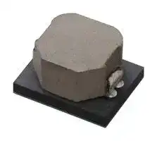
MYSGK4R030ERSR
Non Isolated POL DC/DC Converter, Step Down, Module, 120 W, 700 mV, 4 V, 30 A
⚠️ Reference pricing provided. In case of supply shortages, we will connect you with our trusted procurement partners to ensure your project's continuity.
- Manufacturer: MURATA POWER SOLUTIONS
- Product type: DC / DC Non Isolated Board Mount Converters - Adjustable Output
- SVHC: No SVHC (07-Jul-2017)
- Depth: 14mm
- Width: 11mm
- Height: 8.3mm
- Product Range: MonoBK MYSGK Series
- Output Power Max: 120W
- Output Current Max: 30A
- Output Voltage Max: 4V
- Output Voltage Min: 700mV
- Input Voltage DC Max: 15V
- Input Voltage DC Min: 4.5V
- DC / DC Converter Type: Step Down, Module
- Power Supply Applications: -
- DC / DC Converter Output Type: Adjustable
| Delivery and price | |
|---|---|
| Units per pack | 250 |
| Price | 9.34 € |
| Current stock | 50+ |
| Lead time | 30 days |
Datasheet

**MYSGK4R030ERSR**
## MonoBK™, 30A DC-DC Converter
## **PRODUCT OVERVIEW**
## **Typical unit**
## **FEATURES**
■Settable output voltage from 0.7 to 4.0V
■Wide input voltage range 4.5 to 15V
■Up to 30A of output current
- ■Quick response to load change
- ■Ultra small surface mount package 14.0 x 11.0 x 8.3mm
■Peak efficiency of 97.6% max.
■Outstanding thermal derating performance
- ■Over current protection
The **MYSGK4R030ERSR** is miniature MonoBK™ called “Mono Block”, non-isolated Point-of-Load (PoL) DC-DC power converter for embedded applications. The small form factor measures only 14.0 x 11.0 x 8.3mm. Applications include powering FPGA/CPU’s, datacom/telecom systems, Distributed Bus Architectures (DBA), programmable logic and mixed voltage systems.
The converter has input voltage range from 4.5 to 15.0V and a maximum output current of 30A. Based on a fixed frequency synchronous buck converter switching topology, this high power conversion efficient PoL module features settable output voltage 0.7 to 4.0V, On/Off control and Power Good signal output.
The converter also includes under-voltage lock out (UVLO), output short circuit protection and over-current protection.
- ■On/Off control (Positive logic)
- ■Power Good (PG) signal
## **SIMPLIFIED APPLICATION**
## MYSGK4R030ERSR
**==> picture [336 x 114] intentionally omitted <==**
**----- Start of picture text -----**<br>
Vin Vout<br>ON/OFF<br>+Sense<br>PG<br>Vin N.C. Trim<br>R<br>Cin Cout<br>R<br>-Sense<br>GND<br>GND (Thermal Pad) GND<br>**----- End of picture text -----**<br>
(Typical topology is shown. Murata recommends an external input fuse.)
**http://www.murata.com/products/power**
Export Control Code: X0863 Document No: DC_R220011
MYSGK4R030ERSR A03 Page 1 of 23
**MYSGK4R030ERSR**
## MonoBK™, 30A DC-DC Converter
|**PERFORMANCE SPECIFICATIONS SUMMARY ANDORDERING GUIDE**|**PERFORMANCE SPECIFICATIONS SUMMARY ANDORDERING GUIDE**|**PERFORMANCE SPECIFICATIONS SUMMARY ANDORDERING GUIDE**|**PERFORMANCE SPECIFICATIONS SUMMARY ANDORDERING GUIDE**|**PERFORMANCE SPECIFICATIONS SUMMARY ANDORDERING GUIDE**|**PERFORMANCE SPECIFICATIONS SUMMARY ANDORDERING GUIDE**|**PERFORMANCE SPECIFICATIONS SUMMARY ANDORDERING GUIDE**|**PERFORMANCE SPECIFICATIONS SUMMARY ANDORDERING GUIDE**|**PERFORMANCE SPECIFICATIONS SUMMARY ANDORDERING GUIDE**|**PERFORMANCE SPECIFICATIONS SUMMARY ANDORDERING GUIDE**|**PERFORMANCE SPECIFICATIONS SUMMARY ANDORDERING GUIDE**|**PERFORMANCE SPECIFICATIONS SUMMARY ANDORDERING GUIDE**|**PERFORMANCE SPECIFICATIONS SUMMARY ANDORDERING GUIDE**|**PERFORMANCE SPECIFICATIONS SUMMARY ANDORDERING GUIDE**|
|---|---|---|---|---|---|---|---|---|---|---|---|---|---|
|PART NUMBER|OUTPUT||||||INPUT||||Efficiency<br>[%]|ON/OFF|Package<br>[mm]|
||Vout<br>[V]|Iout(max.)<br>[A]|Power<br>[W]<br>[% of Vout]|R/N(typ.)<br>[% of Vout]|Regulation(typ.)||Vin(typ.)<br>[V]|Range<br>[V]|Iin no load<br>[mA]|Iin full load<br>[A]||||
||||||Line[%]|Load[%]||||||||
|MYSGK4R030ERSR|0.7-4.0<br>(typ.:4.0V)|30|120|1|±1.0|±1.0|12|4.5 - 15|95.3|10.59|94.4|Yes<br>(Positive)|14.0 x 11.0 x 8.3|
|MYSGK4R030ERSRD|0.7-4.0<br>(typ.:4.0V)|30|120|1|±1.0|±1.0|12|4.5 - 15|95.3|10.59|94.4|Yes<br>(Positive)|14.0 x 11.0 x 8.3|
1.All specifications are at typical line voltage, Vout = 4.0V and full load, +25degC unless otherwise noted. Output capacitors are 100uF x 8 ceramics. Input capacitors is 22uF x 2 ceramic and plenty electrolytic capacitors. See detailed specifications. Input and output capacitors are necessary for our test equipment. 2.Use adequate ground plane and copper thickness adjacent to the converter.
**==> picture [103 x 7] intentionally omitted <==**
**----- Start of picture text -----**<br>
PART NUMBER STRUCTURE<br>**----- End of picture text -----**<br>
**==> picture [444 x 96] intentionally omitted <==**
**----- Start of picture text -----**<br>
MY SGK 4R0 30 E R S R D<br>Murata Products Packaging Code<br>Blank : Standard Quantity<br>Maximum Output Current Internal Code Internal Code D : Small Quantity<br>Series Name<br>30 : 30A<br>Sr rryrrr e<br>Maximum Output Voltage Input Voltage Range ON/OFF Control Logic<br>4R0 : 4.0V E : 4.5-15.0V S : Positive Logic<br>**----- End of picture text -----**<br>
## **Product Marking**
Because of the small size of these products, the product marking contains a character-reduced code to indicate the model number and manufacturing date code. Not all items on the marking are always used. Please note that the marking differs from the product photograph. Here is the layout of the Marking .
contains a character-reduced code to indicate the model number **Part Number Product Code** and manufacturing date code. Not all items on the marking are MYSGK4R030ERSR E4 always used. Please note that the marking differs from the product photograph. Here is the layout of the Marking . MYSGK4R030ERSRD E4 ~~a~~ **Layout (reference) Codes (reference)** □ □ Internal Manufacturing code 1 E4 Product code (Please see product code table beside.) E4 Internal Manufacturing code 2 | ~~[de]~~
**http://www.murata.com/products/power**
MYSGK4R030ERSR A03 Page 2 of 23
**MYSGK4R030ERSR**
## MonoBK™, 30A DC-DC Converter
## **FUNCTIONAL SPECIFICATIONS OF MYSGK4R030ERSR (Note 1)**
|**ABSOLUTE MAXIMUM RATINGS**|**Conditions**|**Minimum**|**Typical**<br>~~GO~~|**Maximum**<br>~~GO~~|**Units**|
|---|---|---|---|---|---|
|Input Voltage<br>~~GD~~|~~GD~~|-0.3<br>~~GD~~|~~GD~~<br>~~GO~~|16<br>~~GD~~<br>~~GO~~|V<br>~~GD~~|
|ON/OFF Pin<br>~~GD~~<br>~~GO~~|Power on,referred to -Vin<br>~~GD~~<br>~~GO~~|-0.3<br>~~GD~~<br>~~GO~~|~~GD~~<br>~~GO~~<br>~~GO~~|7.5<br>~~GD~~<br>~~GO~~<br>~~GO~~|V<br>~~GD~~<br>~~GO~~|
|PG/Trim Pins<br>~~GO~~<br>~~DG~~|Power on,referred to -Vin<br>~~GO~~<br>~~DG~~|~~GO~~<br>~~DG~~|Source ONLY<br>~~GO~~<br>~~DG~~|~~GO~~<br>~~DG~~|~~GO~~<br>~~DG~~|
|Vout<br>~~DG~~<br>~~GO~~|~~DG~~<br>~~GO~~|-0.3<br>~~DG~~<br>~~GO~~|~~DG~~<br>~~GO~~|4.4<br>~~DG~~<br>~~GO~~|V<br>~~DG~~<br>~~GO~~|
|Output Current<br>~~GO~~<br>~~GO~~|Current-limited,no damage, short-circuitprotected<br>~~GO~~<br>~~GO~~|0<br>~~GO~~<br>~~GO~~|~~GO~~<br>~~GO~~|30<br>~~GO~~<br>~~GO~~|A<br>~~GO~~<br>~~GO~~|
|Storage Temperature Range<br>~~GO~~<br>~~DG~~|Vin = Zero(nopower)<br>~~GO~~<br>~~DG~~|-40<br>~~GO~~<br>~~DG~~|~~GO~~<br>~~DG~~<br>~~(O~~|125<br>~~GO~~<br>~~DG~~<br>~~(O~~|degC<br>~~GO~~<br>~~DG~~|
|Soldering/ Reflow Temperature<br>~~DG~~<br>~~GO~~<br>~~OO~~|Note 16<br>~~DG~~<br>~~GO~~<br>~~OO~~|~~DG~~<br>~~GO~~<br>~~OO~~|~~DG~~<br>~~GO~~<br>~~(O~~<br>~~OO~~|250<br>~~DG~~<br>~~GO~~<br>~~(O~~<br>~~OO~~|degC<br>~~DG~~<br>~~GO~~<br>~~OO~~|
|Maximum Number of Reflows Allowed<br>~~GO~~<br>~~OO~~|Note 16<br>~~GO~~<br>~~OO~~|~~GO~~<br>~~OO~~|~~GO~~<br>~~(O~~<br>~~OO~~|1<br>~~GO~~<br>~~(O~~<br>~~OO~~|~~GO~~<br>~~OO~~|
|Absolute maximums are stress ratings. Exposure of devices to greater than any of these conditions may adversely affect long-term reliability. Proper operation under conditions other<br>than those listed in the Performance/Functional Specifications Table is not implied or recommended.<br>~~OO~~||||||
|**INPUT**<br>~~OO~~|**Conditions**<br>~~OO~~|**Minimum**<br>~~OO~~|**Typical**<br>~~OO~~|**Maximum**<br>~~OO~~|**Units**<br>~~OO~~|
|Operating Voltage Range<br>~~a~~|Lower limit of Vin depends on Vout.<br>Refer to Voltage Range Graph on page 18<br>~~ee~~|4.5<br>~~ee~~|12<br>~~ee~~|15<br>~~ee~~|V<br>~~ee~~|
|Start-up Threshold<br>~~a~~|Risinginput voltage, Vout=1.8V<br>~~ee~~|~~ee~~|4.25<br>~~ee~~|~~ee~~|V<br>~~ee~~|
||Risinginput voltage, Vout=4.0V<br>~~ee~~<br>~~a~~|~~ee~~<br>~~a~~|4.67<br>~~ee~~<br>~~a~~|~~ee~~<br>~~a~~|V<br>~~ee~~<br>~~a~~|
|Under Voltage Shutdown<br>~~a~~<br>~~GO~~|Note 12<br>~~ee~~<br>~~a~~<br>~~GO~~|~~ee~~<br>~~a~~<br>~~GO~~|4.05<br>~~ee~~<br>~~a~~<br>~~GO~~|~~ee~~<br>~~a~~<br>~~GO~~|V<br>~~ee~~<br>~~a~~<br>~~GO~~|
|Internal Filter Type<br>~~GO~~<br>~~DG~~|~~GO~~<br>~~DG~~|~~GO~~<br>~~DG~~|Capacitive<br>~~GO~~<br>~~DG~~|~~GO~~<br>~~DG~~|~~GO~~<br>~~DG~~|
|Input Current<br>~~DG~~<br>~~PT~~||||||
|Full Load Conditions<br>~~PT~~<br>~~GO~~|Vin=12.0V,Vout=4.0V,Iout=30A<br>~~PT~~<br>~~GO~~|~~PT~~<br>~~GO~~|10.59<br>~~PT~~<br>~~GO~~|~~PT~~<br>~~GO~~|A<br>~~PT~~<br>~~GO~~|
|Low Line<br>~~GO~~<br>~~GO~~|Vin=5.2V,Vout=4.0V,Iout=30A<br>~~GO~~<br>~~GO~~|~~GO~~<br>~~GO~~|24.48<br>~~GO~~<br>~~GO~~|~~GO~~<br>~~GO~~|A<br>~~GO~~<br>~~GO~~|
|No Load Current<br>~~GO~~<br>~~CS~~|Iout=0A,unit=ON<br>~~GO~~<br>~~CS~~|~~GO~~<br>~~CS~~|95.3<br>~~GO~~<br>~~CS~~|~~GO~~<br>~~CS~~|mA<br>~~GO~~<br>~~CS~~|
|**GENERAL and SAFETY**<br>~~CS~~|**Conditions**<br>~~CS~~|**Minimum**<br>~~CS~~|**Typical**<br>~~CS~~|**Maximum**<br>~~CS~~|**Units**<br>~~CS~~|
|Efficiency|Vin=12.0V,Vout=4.0V,Iout=30A<br>~~a~~|~~a~~|94.4<br>~~a~~|~~a~~|%|
||Vin=12.0V,Vout=1.8V,Iout=30A<br>~~a~~<br>~~a~~|~~a~~<br>~~a~~|88.3<br>~~a~~<br>~~a~~|~~a~~<br>~~a~~||
||Vin=5.0V,Vout=1.8V,Iout=30A<br>~~a~~<br>~~a~~|~~a~~<br>~~a~~|89.6<br>~~a~~<br>~~a~~|~~a~~<br>~~a~~||
|Calculated MTBF(Note 3)<br>~~Ge~~|Ta=40degC,Vin=12.0V,Vout=4.0V,Iout=50%<br>~~a~~<br>~~Ge~~|~~a~~<br>~~Oe~~|8,300,000<br>~~a~~<br>~~Oe~~|~~a~~<br>~~Oe~~|hours|
|**DYNAMIC CHARACTERISTICS**<br>~~Ge~~|**Conditions**<br>~~Ge~~|**Minimum**<br>~~Oe~~|**Typical**<br>~~Oe~~<br>~~GO~~|**Maximum**<br>~~Oe~~<br>~~GO~~|**Units**|
|Fixed SwitchingFrequency<br>~~GD~~|~~GD~~|~~GD~~|425<br>~~GD~~<br>~~GO~~<br>~~(OO~~|~~GD~~<br>~~GO~~<br>~~(OO~~|kHz<br>~~GD~~|
|StartupTime(Vin on)<br>~~GD~~<br>~~GO~~|Vout=4.0V(from Vin on to 90% of Vout)<br>~~GD~~<br>~~GO~~|~~GD~~<br>~~GO~~|3.9<br>~~GD~~<br>~~GO~~<br>~~GO~~<br>~~(OO~~<br>~~OO~~|~~GD~~<br>~~GO~~<br>~~GO~~<br>~~(OO~~<br>~~OO~~|ms<br>~~GD~~<br>~~GO~~|
|StartupTime(Remote on)<br>~~GO~~<br>~~GO~~<br>~~ee~~|Vout=4.0V(from Remote on to 90% of Vout)<br>~~GO~~<br>~~GO~~<br>|~~GO~~<br>~~GO~~<br>~~OO~~<br>|2.9<br>~~GO~~<br>~~(OO~~<br>~~GO~~<br>~~OO~~<br>~~OO~~<br>|~~GO~~<br>~~(OO~~<br>~~GO~~<br>~~OO~~<br>~~OO~~<br>|ms<br>~~GO~~<br>~~GO~~<br>|
|Dynamic Load Response<br>~~GO~~<br>~~RD~~<br>~~ee~~|(50 to 100% load step,di/dt)<br>~~GO~~<br>~~RD~~<br>|~~GO~~<br>~~RD~~<br>~~OO~~<br>|0.5<br>~~GO~~<br>~~OO~~<br>~~RD~~<br>~~OO~~<br>|~~GO~~<br>~~OO~~<br>~~RD~~<br>~~OO~~<br>|A/us<br>~~GO~~<br>~~RD~~<br>|
|Dynamic Load Peak Deviation<br>~~RD~~<br>~~ee~~|Vout=1.8V(50 to 100% load step,di/dt),Note 14<br>~~RD~~<br>|~~RD~~<br>~~OO~~<br>|±3.0<br>~~RD~~<br>~~OO~~<br>|~~RD~~<br>~~OO~~<br>|% of Vout<br>~~RD~~<br>|
||Vout=4.0V(50 to 100% load step,di/dt),Note 14<br>~~a~~|~~OO~~<br>~~a~~|±3.0<br>~~OO~~<br>~~a~~|~~OO~~<br>~~a~~|% of Vout<br>~~a~~|
|**FUNCTIONS**<br>~~ee~~|**Conditions**<br>~~a~~|**Minimum**<br>~~OO~~<br>~~a~~|**Typical**<br>~~OO~~<br>~~a~~|**Maximum**<br>~~OO~~<br>~~a~~|**Units**<br>~~a~~|
|Remote On/Off Control(Note 4)||||||
|Logic<br>~~PT~~||||||
|ON State Range<br>~~RG~~|Or left open<br>~~RG~~|1.8<br>~~RG~~|~~RG~~|5.0<br>~~RG~~|V<br>~~RG~~|
|OFF Stage Range<br>~~RG~~<br>~~GO~~|~~RG~~<br>~~GO~~|-0.1<br>~~RG~~<br>~~GO~~|~~RG~~<br>~~GO~~|0.5<br>~~RG~~<br>~~GO~~|V<br>~~RG~~<br>~~GO~~|
|Control Current<br>~~GO~~<br>~~DG~~|Open collector/drain<br>~~GO~~<br>~~DG~~|~~GO~~<br>~~DG~~|~~GO~~<br>~~DG~~|-<br>~~GO~~<br>~~DG~~|mA<br>~~GO~~<br>~~DG~~|
|Power Good Output(Pulled upto 5.0V(typ.)internally)<br>~~PE~~||||||
|PG TRUE(High)<br>~~PE~~<br>~~GG~~|~~PE~~<br>~~GG~~|(95% of target Vout)< Vout <(105% of target Vout)<br>~~PE~~<br>~~GG~~|||~~PE~~<br>~~GG~~|
|PG FALSE(Low)<br>~~FG~~|~~FG~~|Out of above range<br>~~FG~~|||~~FG~~|
**http://www.murata.com/products/power**
MYSGK4R030ERSR A03 Page 3 of 23
**MYSGK4R030ERSR**
## MonoBK™, 30A DC-DC Converter
## **FUNCTIONAL SPECIFICATIONS OF MYSGK4R030ERSR (Note 1)**
|**OUTPUT**|**Conditions**|**Minimum**|**Typical**<br>~~DO~~|**Maximum**<br>~~DO~~|**Units**|
|---|---|---|---|---|---|
|Total Output Power<br>~~CD~~|See Derating<br>~~CD~~|0<br>~~CD~~|~~CD~~<br>~~DO~~|120<br>~~CD~~<br>~~DO~~|W<br>~~CD~~|
|Voltage<br>~~CD~~<br>~~DO~~<br>~~PT~~||||||
|Output Voltage Range<br>~~PT~~<br>~~GD~~|Note 10<br>~~PT~~<br>~~GD~~|0.7<br>~~PT~~<br>~~GD~~|~~PT~~<br>~~GD~~|4.0<br>~~PT~~<br>~~GD~~|V<br>~~PT~~<br>~~GD~~|
|Accuracy (50% load, untrimmed)<br>~~GD~~|Vin=12.0V,Vout=4.0V,Cout=800uF,Ta=25degC<br>~~GD~~<br>~~a~~|±1<br>~~GD~~<br>~~a~~|||% of Vout<br>~~GD~~<br>~~a~~|
||Vin=12.0V,Vout=1.8V,Cout=800uF,Ta=25degC<br>~~a~~<br>~~a~~|±1<br>~~a~~<br>~~a~~|||% of Vout<br>~~a~~<br>~~a~~|
||Vin=5.0V,Vout=1.8V,Cout=800uF,Ta=25degC<br>~~a~~<br>~~a~~|±1<br>~~a~~<br>~~a~~|||% of Vout<br>~~a~~<br>~~a~~|
|Over Voltage Protection<br>~~GG~~|Note 13<br>~~a~~<br>~~GG~~|~~a~~<br>~~GG~~|120<br>~~a~~<br>~~GG~~|~~a~~<br>~~GG~~|% of Vout<br>~~a~~<br>~~GG~~|
|Under Voltage Protection<br>~~GG~~<br>~~GG~~|~~GG~~<br>~~GG~~|~~GG~~<br>~~GG~~|68<br>~~GG~~<br>~~GG~~|~~GG~~<br>~~GG~~|% of Vout<br>~~GG~~<br>~~GG~~|
|Current<br>~~GG~~<br>~~PT~~<br>~~(OO~~||||||
|Output Current Range<br>~~PT~~<br>~~DO~~|Note 2<br>~~PT~~<br>~~DO~~|0<br>~~PT~~<br>~~DO~~|~~PT~~<br>~~DO~~<br>~~(OO~~|30<br>~~PT~~<br>~~DO~~<br>~~(OO~~|A<br>~~PT~~<br>~~DO~~|
|Current Limit Inception<br>~~DO~~<br>~~GO~~|After warm up<br>~~DO~~<br>~~GO~~|~~DO~~<br>~~GO~~|50<br>~~DO~~<br>~~(OO~~<br>~~GO~~|~~DO~~<br>~~(OO~~<br>~~GO~~|A<br>~~DO~~<br>~~GO~~|
|Short Circuit<br>~~GO~~<br>~~GG~~|~~GO~~<br>~~GG~~|~~GO~~<br>~~GG~~|~~GO~~<br>~~GG~~<br>~~(OU~~|~~GO~~<br>~~GG~~<br>~~(OU~~|~~GO~~<br>~~GG~~|
|Short Circuit Duration(remove short for recovery)<br>~~GG~~<br>~~GO~~|Output shorted toground,no damage<br>~~GG~~<br>~~GO~~|~~GG~~<br>~~GO~~|Continuous<br>~~GG~~<br>~~GO~~<br>~~(OU~~|~~GG~~<br>~~GO~~<br>~~(OU~~|~~GG~~<br>~~GO~~|
|Short Circuit Protection Method<br>~~GO~~|Note 5<br>~~GO~~|~~GO~~|Hiccup<br>~~GO~~<br>~~(OU~~|~~GO~~<br>~~(OU~~|~~GO~~|
|Pre-bias Start-up||Converter will start up if the external output voltage is<br>less than set Vout.||||
|Regulation(Note 8)<br>~~pT~~||||||
|Line Regulation<br>~~pT~~<br>~~GO~~|Vin=min. to max.<br>~~pT~~<br>~~GO~~|~~pT~~<br>~~GO~~|±1<br>~~pT~~<br>~~GO~~|~~pT~~<br>~~GO~~|% of Vout<br>~~pT~~<br>~~GO~~|
|Load Regulation<br>~~GO~~<br>~~GG~~|Iout=min. to max.<br>~~GO~~<br>~~GG~~|~~GO~~<br>~~GG~~|±1<br>~~GO~~<br>~~GG~~|~~GO~~<br>~~GG~~|% of Vout<br>~~GO~~<br>~~GG~~|
|Temperature variation<br>~~GG~~<br>~~DG~~|~~GG~~<br>~~DG~~|~~GG~~<br>~~DG~~|±1<br>~~GG~~<br>~~DG~~|~~GG~~<br>~~DG~~|% of Vout<br>~~GG~~<br>~~DG~~|
|Total output voltage variation(Note 15)<br>~~DG~~<br>~~fe~~|Fixed Vin,Iout=min. to max.<br>~~DG~~<br>~~fe~~|~~DG~~<br>~~fe~~|~~DG~~<br>~~fe~~|±3<br>~~DG~~<br>~~fe~~|% of Vout<br>~~DG~~<br>~~fe~~|
|Ripple and Noise(20MHz bandwidth)<br>~~fe~~<br>~~GG~~|Note 6<br>~~fe~~<br>~~GG~~|~~fe~~<br>~~GG~~|1<br>~~fe~~<br>~~GG~~|~~fe~~<br>~~GG~~|% of Vout<br>~~fe~~<br>~~GG~~|
|External Output Capacitance Range(Note 11)<br>~~GG~~<br>~~GG~~|~~GG~~<br>~~GG~~|800<br>~~GG~~<br>~~GG~~|~~GG~~<br>~~GG~~|6000<br>~~GG~~<br>~~GG~~|uF<br>~~GG~~<br>~~GG~~|
|**MECHANICAL(Common)**<br>~~GG~~|**Conditions**<br>~~GG~~|**Minimum**<br>~~GG~~|**Typical**<br>~~GG~~|**Maximum**<br>~~GG~~|**Units**<br>~~GG~~|
|Mechanical Dimension<br>~~a~~|L x W x H<br>~~a~~|14.0(typ.)x 11.0(typ.)x 8.3(max.)<br>~~a~~|||mm<br>~~a~~|
|Weight<br>~~a~~<br>~~GG~~|~~a~~<br>~~GG~~|~~a~~<br>~~GG~~|4.21<br>~~a~~<br>~~GG~~|~~a~~<br>~~GG~~|grams<br>~~a~~<br>~~GG~~|
|**ENVIRONMENTAL(Common)**<br>~~GG~~|**Conditions**<br>~~GG~~|**Minimum**<br>~~GG~~|**Typical**<br>~~GG~~|**Maximum**<br>~~GG~~|**Units**<br>~~GG~~|
|Operating Ambient Temperature Range<br>~~a~~|With Derating (Notes 2,7)<br>~~a~~|-40<br>~~a~~|~~a~~|105<br>~~a~~|degC<br>~~a~~|
|Storage Temperature Range<br>~~a~~<br>~~GO~~|Nopower supply<br>~~a~~<br>~~GO~~|-40<br>~~a~~<br>~~GO~~|~~a~~<br>~~GO~~|125<br>~~a~~<br>~~GO~~|degC<br>~~a~~<br>~~GO~~|
|Thermal Protection/Shutdown<br>~~GO~~<br>~~GG~~|Measured in module(Note 9)<br>~~GO~~<br>~~GG~~|~~GO~~<br>~~GG~~|165<br>~~GO~~<br>~~GG~~|~~GO~~<br>~~GG~~|degC<br>~~GO~~<br>~~GG~~|
|Moisture SensitivityLevel<br>~~GG~~<br>~~CG~~|~~GG~~<br>~~CG~~|3<br>~~GG~~<br>~~CG~~|||~~GG~~<br>~~CG~~|
|**ENVIRONMENTAL VALIATION TESTING(For reference)**<br>~~CG~~||||||
|High Temperature HumidityBias<br>~~|~~|Ta=85degC/85%RH,Vin=15V,Vout=4.0V,No load,1000 hours<br>~~|~~|||||
|High Temperature Bias<br>~~|~~<br>~~Ge~~|Tj=120degC,Vin=12V,Vout=4.0V,Iout with derating,1000 hours<br>~~|~~<br>~~Ge~~|||||
|Temperature Cycling<br>~~De~~|Ta=-40degC/30min.+125degC/30min.,100cycle<br>~~De~~|||||
## **Specification Notes**
(1)Specifications are typical at Ta=25degC, Vin=typical (+12.0V), Vout=typical (+4.0V), full load, external capacitors and natural convection unless otherwise indicated. The converter is tested and specified with external 100uF x 8 ceramic output capacitors, 22uF x 2 ceramic and plenty electrolytic external input capacitors. All capacitors are low ESR types. These capacitors are necessary to accommodate our test equipment and may not be required to achieve specified performance in your applications. However, Murata recommends installation of these capacitors.
(2)Note that Maximum Power Derating curves indicate an average current at typical input voltage. At higher temperatures and/or no airflow, the converter will tolerate brief full current outputs if the total RMS current over time does not exceed the Derating curve.
(3)Mean Time Between Failure is calculated using the Telecordia SR-332 method, +40degC, half output load, natural air convection.
(4)The On/Off Control Input should use either a switch or an open collector/open drain transistor referenced to GND. A logic gate may also be used by applying appropriate external voltages which do not exceed +Vin.
(5)“Hiccup” overcurrent operation repeatedly attempts to restart the converter with a brief, full-current output. If the overcurrent condition still exists, the restart current will be removed and then tried again. This short current pulse prevents overheating and damaging the converter. Once the fault is removed, the converter immediately recovers normal operation.
(6)Output noise may be further reduced by adding an external filter.
(7)The model can be started at Ta=-40degC
(8)Regulation specifications describe the deviation as the line input voltage or output load current is varied from a midpoint value to its extreme.
(9)Thermal Protection/Shutdown temperature is measured with the sensor in the converter.
(10)Do not exceed maximum power specifications when adjusting the output trim. (11)The maximum output capacitive loads depend on the Equivalent Series Resistance (ESR) of the external output capacitor and, to a lesser extent, the distance and series impedance to the load. Larger capacitance will reduce output noise but may change the transient response. Newer ceramic capacitors with very low ESR may require lower capacitor values to avoid instability. Thoroughly test your capacitors in the application. (12)Do not allow the input voltage to degrade lower than the input under-voltage shutdown voltage at all times. Otherwise, you risk having the converter turn off. The under-voltage shutdown is not latching and will attempt to recover when the input is brought back into normal operating range.
(13)The outputs are intended to sink appreciable reverse current.
(14)About di/dt condition, please refer to the table described later.
(15)Ensured by design. Not production tested.
(16)Recommended reflow profile is described in “Soldering Guidelines”.
**http://www.murata.com/products/power**
MYSGK4R030ERSR A03 Page 4 of 23
**MYSGK4R030ERSR**
## MonoBK™, 30A DC-DC Converter
## **Internal Circuit Diagrams**
## **ON/OFF internal circuit diagram and using guide**
**==> picture [458 x 221] intentionally omitted <==**
**----- Start of picture text -----**<br>
Vin<br>©<br>Pull-Up Resistance<br>12kohm( ± 0.5%)<br>ON/OFF<br>Prerrer errr rrrres<br>: poco bececcecen C )<br>.:.:. : .:.:.:.:.:.:::: 1 11 1 1111111111111H1 : ::: : ::::::::::::::: .|__» To ON/OFF terminal of control IC<br>1 :<br>. i : “s<br>Pull-Down Resistance<br>8.2kohm( ± 0.5%)<br>Seeemeeeeeeeee<br>GND<br>Recommended application<br>**----- End of picture text -----**<br>
## **Power Good(PG) internal circuit diagram and using guide**
**==> picture [370 x 213] intentionally omitted <==**
**----- Start of picture text -----**<br>
Vin<br>Regulator<br>Vout from the regulator:5V(typ.) if Vin>5.2V<br>Vout from the regulator:Vin-0.4V to Vin if Vin≦5.2V<br>Source Current<br>100kohm( ± 5%)<br>0.02mA(min.)<br>PG<br>PG<br>Connect to the other Logic Control<br>converter's ON/OFF Circuit<br>Sink Current<br>terminal etc.<br>1.0mA(max.)<br>PG Pull-down FET<br>**----- End of picture text -----**<br>
**http://www.murata.com/products/power**
MYSGK4R030ERSR A03 Page 5 of 23
## **MYSGK4R030ERSR**
## MonoBK™, 30A DC-DC Converter
## **PERFORMANCE DATA AND OSCILLOGRAMS OF MYSGK4R030ERSR**
**==> picture [188 x 172] intentionally omitted <==**
**----- Start of picture text -----**<br>
Efficiency vs. Line Voltage and Load Current at Ta=25degC. (Vout=0.7V)<br>Efficiency<br>30 a el ———<br>_ 85 a<br>= i, |<br>al i i i i 7<br>g ao }---f- (A ee<br>70 se ee ee ee ee ee ee<br>65 toi<br>0 3 6 9 12 15 18 21 24 27 30<br>Output current Iout [A]<br>**----- End of picture text -----**<br>
On/Off Enable Delay (Vin=12.0V, Vout=0.7V, Iout=30A, Cout=800uF) Trace1=ON/OFF, Trace2=Vout, Trace3=PG
**==> picture [57 x 118] intentionally omitted <==**
**----- Start of picture text -----**<br>
ON/OFF 5V/div<br>Vout 1V/div<br>PG 5V/div<br>1ms/div<br>**----- End of picture text -----**<br>
Step Load Transient Response (Vin=12.0V, Vout=0.7V, Cout=800uF, Iout=15 to 30A, 1.0A/us) Trace 3=Vout, 50mV/div, Trace 4=Iout, 20A/div.
**==> picture [185 x 366] intentionally omitted <==**
**----- Start of picture text -----**<br>
Vout vs. Line Voltage and Load Current at Ta=25degC. (Vout=0.7V)<br>Load regulation]<br>CO rerere eg<br>0.707 |<br>re ee ee ee<br>| i i | | H H i i<br>0.700 s | H H H i | |<br>0.686 \ H H \ \ i H i \<br>0.679 ee ee ee ee ee<br>0 3 6 9 12 15 18 21 24 27 30<br>Output current Iout [A]<br>Output Ripple and Noise<br>(Vin=12.0V, Vout=0.7V, Iout=30A, Cout=800uF, Scope BW=20MHz)<br>Prev P p<br>Vout(AC): 5mV/div<br>1us/div<br>Output voltage Vout [V]<br>**----- End of picture text -----**<br>
Step Load Transient Response (Vin=12.0V, Vout=0.7V, Cout=800uF, Iout=30 to 15A, 1.0A/us) Trace 3=Vout, 50mV/div, Trace 4=Iout, 20A/div.
**==> picture [418 x 145] intentionally omitted <==**
**----- Start of picture text -----**<br>
ΔV=32mV<br>ΔV=34mV<br>Vout(AC) 50mV/div<br>pp ee _<br>Vout(AC) 50mV/div<br>Iout 20A/div<br>Iout 20A/div<br>200us/div 200us/div<br>ae<br>**----- End of picture text -----**<br>
## **http://www.murata.com/products/power**
MYSGK4R030ERSR A03 Page 6 of 23
## **MYSGK4R030ERSR**
## MonoBK™, 30A DC-DC Converter
## **PERFORMANCE DATA AND OSCILLOGRAMS OF MYSGK4R030ERSR**
**==> picture [430 x 566] intentionally omitted <==**
**----- Start of picture text -----**<br>
Efficiency vs. Line Voltage and Load Current at Ta=25degC. (Vout=1.8V) Vout vs. Line Voltage and Load Current at Ta=25degC. (Vout=1.8V)<br>Efficiency | Load regulation |<br>100 os - — 1.854 T Tt TT<br>95 f cn ie eed —Vin=4.5V 1.836 ies ee ee<br>F es oe —Viner2v 1200 — — —<br>H } H i H H H | | j | | iH i {<br>70 i i i i i i i i i 4.748 | H i | ! | ! ! |<br>0 3 6 98 12 15 1% 21 24 27 30 0 3 6 9 12 15 18 21 24 27 30<br>Output current Iout [A] Output current Iout [A]<br>On/Off Enable Delay (Vin=12.0V, Vout=1.8V, Iout=30A, Cout=800uF) Output Ripple and Noise<br>Trace1=ON/OFF, Trace2=Vout, Trace3=PG (Vin=12.0V, Vout=1.8V, Iout=30A, Cout=800uF, Scope BW=20MHz)<br>Tek Run Sample 5 Acas Ciena”) Tek Stopped 5197 Acgs<br>LC)<br>ON/OFF 5V/div<br>—<br>Maw(02) 1.924<br>Vout 1V/div<br>Vout(AC): 5mV/div<br>PG 5V/div<br>4a NP OND NIN<br>1ms/div 1us/div<br>Chi 5.0v Ch2 1.04 M 1.0ms SOOkS/s 2.0psipt Chi Somy % Bw MI 1.0us SOOMS/s 2.0nsipt<br>Ch3 5.0¥ A cht + 1.09 A cht + 7O0pY<br>Step Load Transient Response (Vin=12.0V, Vout=1.8V, Cout=800uF, Step Load Transient Response (Vin=12.0V, Vout=1.8V, Cout=800uF,<br>Iout=15 to 30A, 1.0A/us) Trace 3=Vout, 50mV/div, Trace 4=Iout, 20A/div. Iout=30 to 15A, 1.0A/us) Trace 3=Vout, 50mV/div, Trace 4=Iout, 20A/div.<br>Run Sample 629 Acgs Chena”) Tek Run Sample 284 Acgs<br>Ch2 Position<br>ΔV=66mV<br>Ch2 Scale<br>ΔV=68mV 50.0m¥<br>Vout(AC) 50mV/div IMax(c2) —22.0mn¥<br>IMin(C2) ~68.0mY Vout(AC) 50mV/div<br>Iout 20A/div 4 Iout 20A/div<br>200us/div 200us/div<br>Output voltage Vout [V]<br>**----- End of picture text -----**<br>
## **http://www.murata.com/products/power**
MYSGK4R030ERSR A03 Page 7 of 23
## **MYSGK4R030ERSR**
## MonoBK™, 30A DC-DC Converter
## **PERFORMANCE DATA AND OSCILLOGRAMS OF MYSGK4R030ERSR**
**==> picture [188 x 175] intentionally omitted <==**
**----- Start of picture text -----**<br>
Efficiency vs. Line Voltage and Load Current at Ta=25degC. (Vout=2.5V)<br>[Efficiency]<br>100<br>rs<br>ee ee ee —<br>Zo}YA i i} i i<br>52 roPeto ddPo fo PodbPoga ||<br>ifo iot H| | H|' 1 i<br>(rs es ee ee<br>ns re es es |<br>75 :<br>0 3 6 9 12 15 18 21 24 27 3<br>Output current Iout [A]<br>**----- End of picture text -----**<br>
**==> picture [175 x 176] intentionally omitted <==**
**----- Start of picture text -----**<br>
Vout vs. Line Voltage and Load Current at Ta=25degC. (Vout=2.5V)<br>| Load regulation }<br>2.575 T<br>PoP obo UE |<br>v2. oe cee ee<br>obo ob | |<br>2.500 ifreemeni H i i<br>i' ii iH Hli ii |H 1H 1i iH<br>2.450 J—j——4 ff<br>ee ee ee ee ee<br>2.425 . - . . . . . .<br>0 3 6 9 12 158 18 21 24 27 30<br>Output current Iout [A]<br>Output voltage Vout [V]<br>**----- End of picture text -----**<br>
On/Off Enable Delay (Vin=12.0V, Vout=2.5V, Iout=30A, Cout=800uF) Trace1=ON/OFF, Trace2=Vout, Trace3=PG
Output Ripple and Noise (Vin=12.0V, Vout=2.5V, Iout=30A, Cout=800uF, Scope BW=20MHz)
**==> picture [409 x 321] intentionally omitted <==**
**----- Start of picture text -----**<br>
ON/OFF 5V/div<br>IMax(G1) 5.28<br>IMax(G2) 2.8<br>Vout 1V/div<br>IMax(C3)5.4¥<br>PG 5V/div Vout(AC): 5mV/div<br>1ms/div 1us/div<br>oHy ew Che 1.0 AcheM1.0ms+10.0MS/s_—10 100nsipt Chi = 5.0m¥ 4 M1.0usAChl +1.25GS/s1.2mv —-800psipt<br>Step Load Transient Response (Vin=12.0V, Vout=2.5V, Cout=800uF, Step Load Transient Response (Vin=12.0V, Vout=2.5V, Cout=800uF,<br>Iout=15 to 30A, 1.0A/us) Trace 2=Vout, 50mV/div, Trace 4=Iout, 20A/div. Iout=30 to 15A, 1.0A/us) Trace 2=Vout, 50mV/div, Trace 4=Iout, 20A/div.<br>Sample 54 Acqs Melenu Tek = Run Sample 31 Acqs<br>ΔV=88mV<br>ΔV=90mV<br>Vout(AC) 50mV/div IMan(c2)-36.0m¥<br>IMin(c2)—-90.0rn¥” Vout(AC) 50mV/div<br>Iout 20A/div Iout 20A/div<br>200us/div 4 200us/div<br>**----- End of picture text -----**<br>
Step Load Transient Response (Vin=12.0V, Vout=2.5V, Cout=800uF, Iout=15 to 30A, 1.0A/us) Trace 2=Vout, 50mV/div, Trace 4=Iout, 20A/div.
## **http://www.murata.com/products/power**
MYSGK4R030ERSR A03 Page 8 of 23
## **MYSGK4R030ERSR**
## MonoBK™, 30A DC-DC Converter
## **PERFORMANCE DATA AND OSCILLOGRAMS OF MYSGK4R030ERSR**
**==> picture [495 x 178] intentionally omitted <==**
**----- Start of picture text -----**<br>
Efficiency vs. Line Voltage and Load Current at Ta=25degC. (Vout=3.3V) Vout vs. Line Voltage and Load Current at Ta=25degC. (Vout=3.3V)<br>Efficiency Load regulation<br>100 iTtH H7 H7 |YY| |tTi H4 3.398 } ;| |i | ;} |i<br>9 Wit —Vin=4.5V 3.368 ft —Vin=4.5V<br>SSS Poy PP EE P|<br>= 90 | dan teen teeeeen Seeeeen Seeeen Geen toe ee en | , of |<br>>{|||||||<br>S| i | i H H i | Hl H i i Hl H i i i<br>uw | | { | | | { i i i | i i | | {<br>° 0 3 6 9 12 15 18 21 24 27 30 3.201 0 3: 6: 9—12 15 18—_——21 24 27 30<br>Output current Iout [A] Output current Iout [A]<br>Output voltage Vout [V]<br>**----- End of picture text -----**<br>
On/Off Enable Delay (Vin=12.0V, Vout=3.3V, Iout=30A, Cout=800uF) Trace1=ON/OFF, Trace2=Vout, Trace3=PG
Output Ripple and Noise (Vin=12.0V, Vout=3.3V, Iout=30A, Cout=800uF, Scope BW=20MHz)
**==> picture [425 x 330] intentionally omitted <==**
**----- Start of picture text -----**<br>
ON/OFF 5V/div<br>1<br>Max (C1) 3.6Y<br>Vout 1V/div<br>Max (C2) 3.36V<br>4<br>Max (C3) S.4yv<br>2<br>PG 5V/div<br>Vout(AC): 5mV/div<br>1ms/div 1us/div<br>Chi S.0v By Ch2 1.0¥ M 1.0ms 10.0MS/s 100ns/pt Chi S.Om¥ 4 M 1.0ps 1.25GS/s 800psJ/pt<br>Ch3 S.0v By ACh2 + 1.88Y AChT + 1.8m¥<br>Step Load Transient Response (Vin=12.0V, Vout=3.3V, Cout=800uF, Step Load Transient Response (Vin=12.0V, Vout=3.3V, Cout=800uF,<br>Iout=15 to 30A, 1.0A/us) Trace 2=Vout, 100mV/div, Trace 4=Iout, 20A/div. Iout=30 to 15A, 1.0A/us) Trace 2=Vout, 100mV/div, Trace 4=Iout, 20A/div.<br>Run ample AS ery | tee Run sarpte 18 Acgs<br>[ t Ch2 Position +<br>. + 1.0div +t<br>t Ch2 Scale ΔV=112mV +<br>C ΔV=128mV rr 100.0in¥ +<br>[ t Vout(AC) 100mV/div Man (C2) 44.0my t<br>E s Fy a 7 -<br>|—_______) ¥<br>Vout(AC) 100mV/div<br>Debate<br>L + Iout 20A/div Iout 20A/div<br>200us/div 200us/div<br>**----- End of picture text -----**<br>
Step Load Transient Response (Vin=12.0V, Vout=3.3V, Cout=800uF, Iout=30 to 15A, 1.0A/us) Trace 2=Vout, 100mV/div, Trace 4=Iout, 20A/div.
## **http://www.murata.com/products/power**
MYSGK4R030ERSR A03 Page 9 of 23
## **MYSGK4R030ERSR**
## MonoBK™, 30A DC-DC Converter
## **PERFORMANCE DATA AND OSCILLOGRAMS OF MYSGK4R030ERSR**
**==> picture [188 x 177] intentionally omitted <==**
**----- Start of picture text -----**<br>
Efficiency vs. Line Voltage and Load Current at Ta=25degC. (Vout=4.0V)<br>Efficiency<br>100 T T i T T i T 7<br>ee<br>98 }—-}—_' aa | | |Lo|<br>i i i i H i H<br>mee 90 rr ren<br>> Pp<br>e ee ee ee |<br>in&eoO 86 PoEai| {EE| i| el a|i | iHpoi|i iH|<br>PoE<br>0 3 6 9 12 15 18 21 24 27 30<br>Output current Iout [A]<br>**----- End of picture text -----**<br>
On/Off Enable Delay (Vin=12.0V, Vout=4.0V, Iout=30A, Cout=800uF) Trace1=ON/OFF, Trace2=Vout, Trace3=PG
**==> picture [191 x 315] intentionally omitted <==**
**----- Start of picture text -----**<br>
ON/OFF 5V/div<br>1<br>Vout 2V/div<br>PG 5V/div<br>2<br>1ms/div<br>ChiCh3 =| 5.05.0V ByBw Ch2 = 2.0Y M1.0msAch2 +10.0MS/s2.09 — 100ns/pt<br>Step Load Transient Response (Vin=12.0V, Vout=4.0V, Cout=800uF,<br>Iout=15 to 30A, 1.0A/us) Trace 2=Vout, 100mV/div, Trace 4=Iout, 20A/div.<br>Tek Run Sample 71 Acgs<br>f<br>C<br>ΔV=152mV<br>Cri" Vout(AC) 100mV/div<br>f<br>Iout 20A/div<br>at<br>200us/div<br>**----- End of picture text -----**<br>
**==> picture [187 x 563] intentionally omitted <==**
**----- Start of picture text -----**<br>
Vout vs. Line Voltage and Load Current at Ta=25degC. (Vout=4.0V)<br>Load regulation }<br>4.120 H | Hl H | Hl { | |<br>ee ee es ee ee<br>4.080 |ineSS SESSi iSSS Henen i nen i On e i ONE eni i<br>+ + 4 4 +<br>ee ee<br>4.000 fo<br>es ee ee ee ee ee |<br>3.980J ;Po}Ht i| |obiH GoiT| FobitT iPT EdiGEtT i i4<br>3.920 crn Reena nee Gennes eeeeet Senos nee S|<br>0 3 6 9 12 15 18 21 24 27<br>Output current Iout [A]<br>Output Ripple and Noise<br>(Vin=12.0V, Vout=4.0V, Iout=30A, Cout=800uF, Scope BW=20MHz)<br>Tek Stopped Single- Seq 1 Acqs<br>1+1 4 \<br>i<br>Vout(AC): 10mV/div<br>1us/div<br>Ch 10.0m¥ M i.OpsF1250Si600p 00psie<br>Step Load Transient Response (Vin=12.0V, Vout=4.0V, Cout=800uF,<br>Iout=30 to 15A, 1.0A/us) Trace 2=Vout, 100mV/div, Trace 4=Iout, 20A/div.<br>Tek Run Sample 21 Acgs<br>ΔV=144mV<br>Vout(AC) 100mV/div<br>Iout 20A/div<br>4<br>200us/div<br>Output voltage Vout [V]<br>**----- End of picture text -----**<br>
Step Load Transient Response (Vin=12.0V, Vout=4.0V, Cout=800uF, Iout=30 to 15A, 1.0A/us) Trace 2=Vout, 100mV/div, Trace 4=Iout, 20A/div.
## **http://www.murata.com/products/power**
MYSGK4R030ERSR A03 Page 10 of 23
## **MYSGK4R030ERSR**
## MonoBK™, 30A DC-DC Converter
## **THERMAL DERATINGS OF MYSGK4R030ERSR**
**==> picture [139 x 8] intentionally omitted <==**
**----- Start of picture text -----**<br>
Maximum Current Temperature Derating at Sea Level<br>**----- End of picture text -----**<br>
Thermal deratings are evaluated in following conditions.
・The product is mounted on 60.0mm x 50.8mm x 1.6mm (8 Layer, 2oz copper each) FR-4 board respectively. ・No forced air flow.
Surface(Top of the coil) temperature of the product : 115degC(max.)
## **TRANSIENT RESPONSE DATAS OF MYSGK4R030ERSR**
Transient response data at various conditions are showed in following table. Minimum output capacitance can serve less than 3% of Vout of deviation for 15A load change(0.5A/us).
|Part Number|Vin [V]|Vout [V]|Cout [uF]|Voltage Deviation[mV]|
|---|---|---|---|---|
|||||15-30A Load Step (0.5A/us)|
|MYSGK4R030ERSR|5|0.7|800|20|
|||1.8||45|
|||2.5||72|
|||3.3||96|
||12|0.7|800|20|
|||1.8||46|
|||2.5||72|
|||3.3||96|
|||4.0||120|
**http://www.murata.com/products/power**
MYSGK4R030ERSR A03 Page 11 of 23
**MYSGK4R030ERSR**
## MonoBK™, 30A DC-DC Converter
## **MECHANICAL SPECIFICATIONS**
## **Dimension and Pin Assignment**
## < Top View >
## < Bottom View >
1 Pin (back side)
Unit: mm Tolerances `±` 0.25mm
## < Side View >
|**INPUT/OUTPUT CONNECTIONS**|**INPUT/OUTPUT CONNECTIONS**|
|---|---|
|Pin No.|Function|
|1-9|GND|
|10-18|Vout|
|19|+Sense|
|20|Trim|
|21|-Sense|
|22-30|GND|
|31-39|Vin|
|40|ON/OFF|
|41|N.C.|
|42|Power Good|
|43-54<br>~~※”N.C.” is recommended to be open.~~|GND(Thermal<br>Pad)<br>~~”N.C.” is recommended to be open.~~|
**http://www.murata.com/products/power**
MYSGK4R030ERSR A03 Page 12 of 23
## **MYSGK4R030ERSR**
## MonoBK™, 30A DC-DC Converter
## **Recommended Board Land Pattern (Top View)**
||1.3<br>1.3<br>1.3<br>1.4<br>0.2<br>1.3<br>1.3<br>1.3<br>0.2<br>0.2<br>0.2|1.3<br>1.3<br>1.3<br>1.4<br>0.2<br>1.3<br>1.3<br>1.3<br>0.2<br>0.2<br>0.2|18<br>15<br>12<br>17<br>14<br>11<br>19<br>21<br>42<br>40<br>48<br>44<br>47<br>50<br>0.9<br>1.3<br>1.3<br>1.3<br>0.9<br>0.2<br>0.2<br>49<br>46<br>1.1<br>0.2<br>1.1<br>0.2<br>1.1<br>20<br>41<br>51<br>53<br>52<br>16<br>13<br>10<br>9<br>6<br>3<br>8<br>5<br>2<br>7<br>4<br>39<br>36<br>33<br>38<br>35<br>32<br>37<br>34<br>31<br>30<br>27<br>24<br>29<br>26<br>23<br>28<br>25<br>22<br>0.2<br>1.3<br>1.2<br>1.2<br>54<br>0.7<br>0.5<br>45<br>1<br>43|18<br>15<br>12<br>17<br>14<br>11<br>19<br>21<br>42<br>40<br>48<br>44<br>47<br>50<br>0.9<br>1.3<br>1.3<br>1.3<br>0.9<br>0.2<br>0.2<br>49<br>46<br>1.1<br>0.2<br>1.1<br>0.2<br>1.1<br>20<br>41<br>51<br>53<br>52<br>16<br>13<br>10<br>9<br>6<br>3<br>8<br>5<br>2<br>7<br>4<br>39<br>36<br>33<br>38<br>35<br>32<br>37<br>34<br>31<br>30<br>27<br>24<br>29<br>26<br>23<br>28<br>25<br>22<br>0.2<br>1.3<br>1.2<br>1.2<br>54<br>0.7<br>0.5<br>45<br>1<br>43|18<br>15<br>12<br>17<br>14<br>11<br>19<br>21<br>42<br>40<br>48<br>44<br>47<br>50<br>0.9<br>1.3<br>1.3<br>1.3<br>0.9<br>0.2<br>0.2<br>49<br>46<br>1.1<br>0.2<br>1.1<br>0.2<br>1.1<br>20<br>41<br>51<br>53<br>52<br>16<br>13<br>10<br>9<br>6<br>3<br>8<br>5<br>2<br>7<br>4<br>39<br>36<br>33<br>38<br>35<br>32<br>37<br>34<br>31<br>30<br>27<br>24<br>29<br>26<br>23<br>28<br>25<br>22<br>0.2<br>1.3<br>1.2<br>1.2<br>54<br>0.7<br>0.5<br>45<br>1<br>43|18<br>15<br>12<br>17<br>14<br>11<br>19<br>21<br>42<br>40<br>48<br>44<br>47<br>50<br>0.9<br>1.3<br>1.3<br>1.3<br>0.9<br>0.2<br>0.2<br>49<br>46<br>1.1<br>0.2<br>1.1<br>0.2<br>1.1<br>20<br>41<br>51<br>53<br>52<br>16<br>13<br>10<br>9<br>6<br>3<br>8<br>5<br>2<br>7<br>4<br>39<br>36<br>33<br>38<br>35<br>32<br>37<br>34<br>31<br>30<br>27<br>24<br>29<br>26<br>23<br>28<br>25<br>22<br>0.2<br>1.3<br>1.2<br>1.2<br>54<br>0.7<br>0.5<br>45<br>1<br>43|18<br>15<br>12<br>17<br>14<br>11<br>19<br>21<br>42<br>40<br>48<br>44<br>47<br>50<br>0.9<br>1.3<br>1.3<br>1.3<br>0.9<br>0.2<br>0.2<br>49<br>46<br>1.1<br>0.2<br>1.1<br>0.2<br>1.1<br>20<br>41<br>51<br>53<br>52<br>16<br>13<br>10<br>9<br>6<br>3<br>8<br>5<br>2<br>7<br>4<br>39<br>36<br>33<br>38<br>35<br>32<br>37<br>34<br>31<br>30<br>27<br>24<br>29<br>26<br>23<br>28<br>25<br>22<br>0.2<br>1.3<br>1.2<br>1.2<br>54<br>0.7<br>0.5<br>45<br>1<br>43|18<br>15<br>12<br>17<br>14<br>11<br>19<br>21<br>42<br>40<br>48<br>44<br>47<br>50<br>0.9<br>1.3<br>1.3<br>1.3<br>0.9<br>0.2<br>0.2<br>49<br>46<br>1.1<br>0.2<br>1.1<br>0.2<br>1.1<br>20<br>41<br>51<br>53<br>52<br>16<br>13<br>10<br>9<br>6<br>3<br>8<br>5<br>2<br>7<br>4<br>39<br>36<br>33<br>38<br>35<br>32<br>37<br>34<br>31<br>30<br>27<br>24<br>29<br>26<br>23<br>28<br>25<br>22<br>0.2<br>1.3<br>1.2<br>1.2<br>54<br>0.7<br>0.5<br>45<br>1<br>43|18<br>15<br>12<br>17<br>14<br>11<br>19<br>21<br>42<br>40<br>48<br>44<br>47<br>50<br>0.9<br>1.3<br>1.3<br>1.3<br>0.9<br>0.2<br>0.2<br>49<br>46<br>1.1<br>0.2<br>1.1<br>0.2<br>1.1<br>20<br>41<br>51<br>53<br>52<br>16<br>13<br>10<br>9<br>6<br>3<br>8<br>5<br>2<br>7<br>4<br>39<br>36<br>33<br>38<br>35<br>32<br>37<br>34<br>31<br>30<br>27<br>24<br>29<br>26<br>23<br>28<br>25<br>22<br>0.2<br>1.3<br>1.2<br>1.2<br>54<br>0.7<br>0.5<br>45<br>1<br>43|18<br>15<br>12<br>17<br>14<br>11<br>19<br>21<br>42<br>40<br>48<br>44<br>47<br>50<br>0.9<br>1.3<br>1.3<br>1.3<br>0.9<br>0.2<br>0.2<br>49<br>46<br>1.1<br>0.2<br>1.1<br>0.2<br>1.1<br>20<br>41<br>51<br>53<br>52<br>16<br>13<br>10<br>9<br>6<br>3<br>8<br>5<br>2<br>7<br>4<br>39<br>36<br>33<br>38<br>35<br>32<br>37<br>34<br>31<br>30<br>27<br>24<br>29<br>26<br>23<br>28<br>25<br>22<br>0.2<br>1.3<br>1.2<br>1.2<br>54<br>0.7<br>0.5<br>45<br>1<br>43|18<br>15<br>12<br>17<br>14<br>11<br>19<br>21<br>42<br>40<br>48<br>44<br>47<br>50<br>0.9<br>1.3<br>1.3<br>1.3<br>0.9<br>0.2<br>0.2<br>49<br>46<br>1.1<br>0.2<br>1.1<br>0.2<br>1.1<br>20<br>41<br>51<br>53<br>52<br>16<br>13<br>10<br>9<br>6<br>3<br>8<br>5<br>2<br>7<br>4<br>39<br>36<br>33<br>38<br>35<br>32<br>37<br>34<br>31<br>30<br>27<br>24<br>29<br>26<br>23<br>28<br>25<br>22<br>0.2<br>1.3<br>1.2<br>1.2<br>54<br>0.7<br>0.5<br>45<br>1<br>43|18<br>15<br>12<br>17<br>14<br>11<br>19<br>21<br>42<br>40<br>48<br>44<br>47<br>50<br>0.9<br>1.3<br>1.3<br>1.3<br>0.9<br>0.2<br>0.2<br>49<br>46<br>1.1<br>0.2<br>1.1<br>0.2<br>1.1<br>20<br>41<br>51<br>53<br>52<br>16<br>13<br>10<br>9<br>6<br>3<br>8<br>5<br>2<br>7<br>4<br>39<br>36<br>33<br>38<br>35<br>32<br>37<br>34<br>31<br>30<br>27<br>24<br>29<br>26<br>23<br>28<br>25<br>22<br>0.2<br>1.3<br>1.2<br>1.2<br>54<br>0.7<br>0.5<br>45<br>1<br>43|18<br>15<br>12<br>17<br>14<br>11<br>19<br>21<br>42<br>40<br>48<br>44<br>47<br>50<br>0.9<br>1.3<br>1.3<br>1.3<br>0.9<br>0.2<br>0.2<br>49<br>46<br>1.1<br>0.2<br>1.1<br>0.2<br>1.1<br>20<br>41<br>51<br>53<br>52<br>16<br>13<br>10<br>9<br>6<br>3<br>8<br>5<br>2<br>7<br>4<br>39<br>36<br>33<br>38<br>35<br>32<br>37<br>34<br>31<br>30<br>27<br>24<br>29<br>26<br>23<br>28<br>25<br>22<br>0.2<br>1.3<br>1.2<br>1.2<br>54<br>0.7<br>0.5<br>45<br>1<br>43|18<br>15<br>12<br>17<br>14<br>11<br>19<br>21<br>42<br>40<br>48<br>44<br>47<br>50<br>0.9<br>1.3<br>1.3<br>1.3<br>0.9<br>0.2<br>0.2<br>49<br>46<br>1.1<br>0.2<br>1.1<br>0.2<br>1.1<br>20<br>41<br>51<br>53<br>52<br>16<br>13<br>10<br>9<br>6<br>3<br>8<br>5<br>2<br>7<br>4<br>39<br>36<br>33<br>38<br>35<br>32<br>37<br>34<br>31<br>30<br>27<br>24<br>29<br>26<br>23<br>28<br>25<br>22<br>0.2<br>1.3<br>1.2<br>1.2<br>54<br>0.7<br>0.5<br>45<br>1<br>43|18<br>15<br>12<br>17<br>14<br>11<br>19<br>21<br>42<br>40<br>48<br>44<br>47<br>50<br>0.9<br>1.3<br>1.3<br>1.3<br>0.9<br>0.2<br>0.2<br>49<br>46<br>1.1<br>0.2<br>1.1<br>0.2<br>1.1<br>20<br>41<br>51<br>53<br>52<br>16<br>13<br>10<br>9<br>6<br>3<br>8<br>5<br>2<br>7<br>4<br>39<br>36<br>33<br>38<br>35<br>32<br>37<br>34<br>31<br>30<br>27<br>24<br>29<br>26<br>23<br>28<br>25<br>22<br>0.2<br>1.3<br>1.2<br>1.2<br>54<br>0.7<br>0.5<br>45<br>1<br>43|18<br>15<br>12<br>17<br>14<br>11<br>19<br>21<br>42<br>40<br>48<br>44<br>47<br>50<br>0.9<br>1.3<br>1.3<br>1.3<br>0.9<br>0.2<br>0.2<br>49<br>46<br>1.1<br>0.2<br>1.1<br>0.2<br>1.1<br>20<br>41<br>51<br>53<br>52<br>16<br>13<br>10<br>9<br>6<br>3<br>8<br>5<br>2<br>7<br>4<br>39<br>36<br>33<br>38<br>35<br>32<br>37<br>34<br>31<br>30<br>27<br>24<br>29<br>26<br>23<br>28<br>25<br>22<br>0.2<br>1.3<br>1.2<br>1.2<br>54<br>0.7<br>0.5<br>45<br>1<br>43|18<br>15<br>12<br>17<br>14<br>11<br>19<br>21<br>42<br>40<br>48<br>44<br>47<br>50<br>0.9<br>1.3<br>1.3<br>1.3<br>0.9<br>0.2<br>0.2<br>49<br>46<br>1.1<br>0.2<br>1.1<br>0.2<br>1.1<br>20<br>41<br>51<br>53<br>52<br>16<br>13<br>10<br>9<br>6<br>3<br>8<br>5<br>2<br>7<br>4<br>39<br>36<br>33<br>38<br>35<br>32<br>37<br>34<br>31<br>30<br>27<br>24<br>29<br>26<br>23<br>28<br>25<br>22<br>0.2<br>1.3<br>1.2<br>1.2<br>54<br>0.7<br>0.5<br>45<br>1<br>43|18<br>15<br>12<br>17<br>14<br>11<br>19<br>21<br>42<br>40<br>48<br>44<br>47<br>50<br>0.9<br>1.3<br>1.3<br>1.3<br>0.9<br>0.2<br>0.2<br>49<br>46<br>1.1<br>0.2<br>1.1<br>0.2<br>1.1<br>20<br>41<br>51<br>53<br>52<br>16<br>13<br>10<br>9<br>6<br>3<br>8<br>5<br>2<br>7<br>4<br>39<br>36<br>33<br>38<br>35<br>32<br>37<br>34<br>31<br>30<br>27<br>24<br>29<br>26<br>23<br>28<br>25<br>22<br>0.2<br>1.3<br>1.2<br>1.2<br>54<br>0.7<br>0.5<br>45<br>1<br>43|18<br>15<br>12<br>17<br>14<br>11<br>19<br>21<br>42<br>40<br>48<br>44<br>47<br>50<br>0.9<br>1.3<br>1.3<br>1.3<br>0.9<br>0.2<br>0.2<br>49<br>46<br>1.1<br>0.2<br>1.1<br>0.2<br>1.1<br>20<br>41<br>51<br>53<br>52<br>16<br>13<br>10<br>9<br>6<br>3<br>8<br>5<br>2<br>7<br>4<br>39<br>36<br>33<br>38<br>35<br>32<br>37<br>34<br>31<br>30<br>27<br>24<br>29<br>26<br>23<br>28<br>25<br>22<br>0.2<br>1.3<br>1.2<br>1.2<br>54<br>0.7<br>0.5<br>45<br>1<br>43|18<br>15<br>12<br>17<br>14<br>11<br>19<br>21<br>42<br>40<br>48<br>44<br>47<br>50<br>0.9<br>1.3<br>1.3<br>1.3<br>0.9<br>0.2<br>0.2<br>49<br>46<br>1.1<br>0.2<br>1.1<br>0.2<br>1.1<br>20<br>41<br>51<br>53<br>52<br>16<br>13<br>10<br>9<br>6<br>3<br>8<br>5<br>2<br>7<br>4<br>39<br>36<br>33<br>38<br>35<br>32<br>37<br>34<br>31<br>30<br>27<br>24<br>29<br>26<br>23<br>28<br>25<br>22<br>0.2<br>1.3<br>1.2<br>1.2<br>54<br>0.7<br>0.5<br>45<br>1<br>43|18<br>15<br>12<br>17<br>14<br>11<br>19<br>21<br>42<br>40<br>48<br>44<br>47<br>50<br>0.9<br>1.3<br>1.3<br>1.3<br>0.9<br>0.2<br>0.2<br>49<br>46<br>1.1<br>0.2<br>1.1<br>0.2<br>1.1<br>20<br>41<br>51<br>53<br>52<br>16<br>13<br>10<br>9<br>6<br>3<br>8<br>5<br>2<br>7<br>4<br>39<br>36<br>33<br>38<br>35<br>32<br>37<br>34<br>31<br>30<br>27<br>24<br>29<br>26<br>23<br>28<br>25<br>22<br>0.2<br>1.3<br>1.2<br>1.2<br>54<br>0.7<br>0.5<br>45<br>1<br>43|
|---|---|---|---|---|---|---|---|---|---|---|---|---|---|---|---|---|---|---|---|---|---|
|||||1||||||||||||||||||
|||||||||||||||||||||||
|||||||||||||||||||||||
|||||7||||||||||||||||||
|||||||||||||||||||||||
|||||10||||||||||||||||||
|||||||||||52||||54||||||||
|||||||||||||||||||||||
|||||13||||||||||||||||||
|||||||||||||||||||||||
|||||||||||19<br>21<br>1.1<br>0.2<br>1.1<br>0.2<br>1.1<br>20||||||||||||
|||||||||||||||||||||||
|||||16||17||18||19||20||21|||28||29||30|
|||||||||||||||||||||||
|0.5||||||||||||||||||||||
|||||||||||||||||||||||
Unit: mm
## **Example of Pattern Layout (Top View)**
**==> picture [203 x 159] intentionally omitted <==**
**----- Start of picture text -----**<br>
Picture 30.8 x 13.0(mm)<br>TOP VIEW<br>—<br>re, te SA<br>mo | |<br>et aeroe M4at i pe:<br>ee ie<br>ml Zz<br>eB RS<br>BOTTOM VIEW<br>**----- End of picture text -----**<br>
## **http://www.murata.com/products/power**
MYSGK4R030ERSR A03 Page 13 of 23
**MYSGK4R030ERSR**
## MonoBK™, 30A DC-DC Converter
## **Application Circuit and BOM list (Evaluation board)**
**==> picture [511 x 448] intentionally omitted <==**
**----- Start of picture text -----**<br>
+Sense<br>Vin-sense Vout-Sense<br>Vin Vout<br>Vin ON/OFF R1 VOUT<br>+Sense<br>PG<br>N.C.<br>WT + Trim TTT” +<br>R2<br>C21 C1 C2 C11 C12 C31 C32 R11 C3 C4 C5 C6 C7 C8 C9 C10 C36,37 C13-16 C23-26<br>R12<br>-Sense<br>GND R13 GND<br>GND<br>wh GND (Thermal Pad) GND THE<br>GND-sense GND-Sense<br>MYSGK4R030ERSR<br>C1, C2 22uF/25V GRM32ER71E226KE15<br>(Murata)<br>C3-10 100uF/6.3V GRM32EE70J107ME15<br>(Murata)<br>R1, R13 1608M, Chip resistor, 0ohm<br>R11, R12 1608M, Chip resistor for trimming<br>C11, C12, C21, C23-26, C31, C32, No mount<br>C36, C37, R2<br>ON/OFF PWGOOD -Sense<br>**----- End of picture text -----**<br>
**http://www.murata.com/products/power**
MYSGK4R030ERSR A03 Page 14 of 23
## **MYSGK4R030ERSR**
## MonoBK™, 30A DC-DC Converter
## **TAPE AND REEL INFORMATION**
**==> picture [71 x 11] intentionally omitted <==**
**----- Start of picture text -----**<br>
Tape Dimension<br>**----- End of picture text -----**<br>
Unit: mm
## **Reel Dimension**
**==> picture [392 x 237] intentionally omitted <==**
**----- Start of picture text -----**<br>
33.5±1.0<br>A<br>2.0±0.5<br>Indication<br>sant<br>φ21.0±0.8 φ13.0±0.5<br>Unit: mm<br>Portion A<br>100±1 330±2<br>φ φ<br>**----- End of picture text -----**<br>
**http://www.murata.com/products/power**
MYSGK4R030ERSR A03 Page 15 of 23
**MYSGK4R030ERSR**
MonoBK™, 30A DC-DC Converter
**==> picture [479 x 159] intentionally omitted <==**
**----- Start of picture text -----**<br>
ies TAPE SPECIFICATIONS esi<br>Empty portion Empty portion Leader portion<br>(200mm Min.) (180mm Min.) (200mm Min.)<br>"Module on tape" portion<br>V AR Y<br>Indication<br>**----- End of picture text -----**<br>
**==> picture [178 x 15] intentionally omitted <==**
**----- Start of picture text -----**<br>
Φ1.5mm hole side<br>No.1 Pin<br>**----- End of picture text -----**<br>
Pulling direction
## **Note**
1. The adhesive strength of the protective tape must be within 0.3-1.0N.
2. Each reel contains the quantities such as the table below.
3. Each reel set in moisture-proof packaging because of MSL 3.
4. No vacant pocket in “Module on tape” section.
5. The reel is labeled with Murata part number and quantity.
6. The color of reel is not specified.
|Part Number|Quantity|
|---|---|
|MYSGK4R030ERSR|150|
|MYSGK4R030ERSRD|50|
**http://www.murata.com/products/power**
MYSGK4R030ERSR A03 Page 16 of 23
**MYSGK4R030ERSR**
## MonoBK™, 30A DC-DC Converter
## **TECHNICAL NOTES**
## **Input Fuse**
Certain applications and/or safety agencies may require fuses at the inputs of power conversion components. Fuses should also be used when there is the possibility of sustained input voltage reversal which is not current limited. For greatest safety, we recommend a fast blow fuse installed in the ungrounded input supply line. The installer must observe all relevant safety standards and regulations. For safety agency approvals, install the converter in compliance with the end-user safety standard. **Input Under-Voltage Shutdown and Start-Up Threshold** Under normal start-up conditions, converters will not begin to regulate properly until the ramping-up input voltage exceeds and remains at the Start-Up Threshold Voltage (see Specifications). Once operating, converters will not turn off until the input voltage drops below the UnderVoltage Shutdown Limit. Subsequent restart will not occur until the input voltage rises again above the Start-Up Threshold. This built-in hysteresis prevents any unstable on/off operation at a single input voltage. Users should be aware however of input sources near the Under-Voltage Shutdown whose voltage decays as input current is consumed (such as capacitor inputs), the converter shuts off and then restarts as the external capacitor recharges. Such situations could oscillate. To prevent this, make sure the operating input voltage is well above the UV Shutdown voltage at all times.
## **Start-Up Time**
Assuming that the output current is set at the rated maximum, the Vin to Vout Start-Up Time (see Specifications) is the time interval between the point when the ramping input voltage crosses the Start-Up Threshold and the fully loaded regulated output voltage enters and remains within its specified accuracy band. Actual measured times will vary with input source impedance, external input capacitance, input voltage slew rate and final value of the input voltage as it appears at the converter. These converters include a soft start circuit to moderate the duty cycle of its PWM controller at power up, thereby limiting the input inrush current. The On/Off Remote Control interval from On command to Vout regulated assumes that the converter already has its input voltage stabilized above the Start-Up Threshold before the On command. The interval is measured from the On command until the output enters and remains within its specified accuracy band. The specification assumes that the output is fully loaded at maximum rated current. Similar conditions apply to the On to Vout regulated specification such as external load capacitance and soft start circuitry.
## **Recommended Input Filtering**
The user must assure that the input source has low AC impedance to provide dynamic stability and that the input supply has little or no inductive content, including long distributed wiring to a remote power supply. For best performance, we recommend installing a low-ESR capacitor immediately adjacent to the converter’s input terminals. The capacitor should be a ceramic type such as the Murata GRM32 series and a electrolytic type such as Panasonic OS-CON series.
Initial suggested capacitor values are 22uF x 2 ceramic type and 1000uF x 1 electrolytic type , rated at twice the expected maximum input voltage. Make sure that the input terminals do not go below the under voltage shutdown voltage at all times. More input bulk capacitance may be added in parallel (either electrolytic or tantalum) if needed.
## **Recommended Output Filtering**
The converter will achieve its rated output ripple and noise with additional external capacitor. The user may install more external output capacitance reduce the ripple even further or for improved dynamic response. Again, use low-ESR ceramic (Murata GRM32 series). Initial values of 100uF x 8 ceramic type may be tried, either single or multiple capacitors in parallel. Mount these close to the converter. Measure the output ripple under your load conditions. Use only as much capacitance as required to achieve your ripple and noise objectives. Excessive capacitance can make step load recovery sluggish or possibly introduce instability. Do not exceed the maximum rated output capacitance listed in the specifications.
## **Output Noise**
All models in this converter series are tested and specified for output noise using designated external input/output components, circuits and layout as shown in the figures below. In the figure below, the two copper strips simulate real-world printed circuit impedances between the power supply and its load. In order to minimize circuit errors and standardize tests between units, scope measurements should be made using BNC connectors or the probe ground should not exceed one half inch and soldered directly to the test circuit.
C1=100uF x 8 CERAMIC
C2=OPEN
Figure :Measuring Output Ripple and Noise
## **Minimum Output Loading Requirements**
All models regulate within specification and are stable under no load to full load conditions. Operation under no load might however slightly increase output ripple and noise.
## **Thermal Shutdown**
To prevent many over temperature problems and damage, these converters include thermal shutdown circuitry. If environmental conditions cause the temperature of the converter’s to rise above the Operating Temperature Range up to the shutdown temperature, an on-board electronic temperature sensor will power down the unit. When the temperature decreases below the turn-on threshold, the converter will automatically restart.
**http://www.murata.com/products/power**
MYSGK4R030ERSR A03 Page 17 of 23
**MYSGK4R030ERSR**
## MonoBK™, 30A DC-DC Converter
**CAUTION:** If you operate too close to the thermal limits, the converter may shut down suddenly without warning. Be sure to thoroughly you’re your application to avoid unplanned thermal shutdown.
## **Temperature Derating Curves**
The graphs in this data sheet illustrate typical operation under a variety of conditions. The derating curves show the maximum continuous ambient air temperature. Note that these are AVERAGE measurements.
Note that the temperatures are of the ambient airflow, not the converter itself which is obviously running at higher temperature than the outside air. Also note that very low flow rates (below about 25 LFM) are similar to “natural convection,” that is, not using fan-forced airflow. Murata makes Characterization measurements in a closed cycle wind tunnel with calibrated airflow. We use both thermocouples and an infrared camera system to observe thermal performance. **CAUTION:** These graphs are all collected at slightly above Sea Level altitude. Be sure to reduce the derating for higher density altitude.
## **Output Current Limiting**
Current limiting inception is defined as the point at which full power falls below the rated tolerance. See the Performance/Functional Specifications. Note particularly that the output current may briefly rise above its rated value in normal operation as long as the average output power is not exceeded. This enhances reliability and continued operation of your application. If the output current is too high, the converter will enter the short circuit condition.
## **Output Short Circuit Condition**
When a converter is in current-limit mode, the output voltage will drop as the output current demand increases. Following a timeout period, the converter will restart, causing the output voltage to begin ramping up to its appropriate value. If the short-circuit condition persists, another shutdown cycle will initiate. This rapid on/off cycling is called “hiccup mode”. The hiccup cycling reduces the average output current, thereby preventing excessive internal temperatures and/or component damage. A short circuit can be tolerated indefinitely. The “hiccup” system differs from older latching short circuit systems because you do not have to power down the converter to make it restart. The system will automatically restore operation as soon as the short circuit condition is removed.
## **UVP/OVP Function**
This product monitors a feedback voltage to detect over and under voltage. When the feedback voltage becomes lower than 68% of the target voltage, after 1ms, the product latches OFF. This function is enables after soft-start is complete.
When the feedback voltage becomes higher than 120% of the target voltage, the circuit operates sink-mode to decrease output voltage until reaching a negative current limit (-49A typ.). Upon reaching the negative current limit, sink-mode is turned off and the device restarts for a short time. The device operates in this cycle until the output voltage is pulled down under the UVP threshold voltage for 1ms. After the 1ms, the circuit latches into sink-mode. The fault is cleared with a reset of Vin or by resetting the ON/OFF pin.
## **Remote On/Off Control**
Please refer to the Connection Diagram on page 1 for On/Off connections.
Positive logic models are enabled when the On/Off pin is left open or is pulled high to Vin with respect to GND. An internal bias current causes the open pin to rise to Vin. Positivepolarity devices are disabled when the On/Off is grounded or brought to within a low voltage (see Specifications) with respect to GND.
Dynamic control of the On/Off function should be able to sink appropriate signal current when brought low and withstand appropriate voltage when brought high. Be aware too that there is a finite time in milliseconds (see Specifications) between the time of On/Off Control activation and stable, regulated output. This time will vary slightly with output load type and current and input conditions.
## **Output Capacitive Load**
Users should only consider adding capacitance to reduce switching noise and/or to handle spike current load steps. Install only enough capacitance to achieve noise objectives. Excess external capacitance may cause regulation problems, degraded transient response and possible oscillation or instability.
## **Soldering Guidelines**
Murata recommends the specifications below when installing these converters. These specifications vary depending on the solder type.
Exceeding these specifications may cause damage to the product. Your production environment may differ therefore please thoroughly review these guidelines with your process engineers. This product can be reflowed once.
|**Reflow Solder Operations for surface-mountproducts**|**Reflow Solder Operations for surface-mountproducts**|
|---|---|
|For Sn/Ag/Cu based solders:||
|Preheat Temperature|Less than 1degCper second|
|Time over Liquidus|45 to 75 seconds|
|Maximum Peak Temperature|250degC|
|CoolingRate|Less than 3degCper second|
|For Sn/Pb based solders:||
|Preheat Temperature|Less than 1degCper second|
|Time over Liquidus|60 to 75 seconds|
|Maximum Peak Temperature|235degC|
|CoolingRate|Less than 3degCper second|
**http://www.murata.com/products/power**
MYSGK4R030ERSR A03 Page 18 of 23
**MYSGK4R030ERSR**
## MonoBK™, 30A DC-DC Converter
## **Recommended Lead-free Solder Reflow Profile**
## **Output Voltage Adjustment**
The output voltage may be adjusted over a limited range by connecting an external trim resistor (Rtrim) between the Trim pin and GND pin. The Rtrim resistor must be a 1/10W precision metal film type, `±` 0.5% accuracy or better with low temperature coefficient, `±` 100ppm/degC or better. Mount the resistor close to the converter with very short leads or use a surface mount trim resistor.
In the table below, the estimated resistance is given at limited condition ; Vin : typ., Ta : 25degC, Iout : max., Cout : 800uF. (Please look at Test Circuit which is shown below). Do not exceed the specified limits of the output voltage or the converter’s maximum power rating when applying these resistors. Also, avoid high noise at the Trim input. However, to prevent instability, you should never connect any capacitors between Trim pin and GND pin.
**CAUTION: Do not reflow the converter as follows, because the converter may fall from the substrate during reflowing.**
||||||**Estimated Rtrim[kohm]**|
|---|---|---|---|---|---|
|**Output Voltage**|||||**MYSGK4R030ERSR**|
|0.7V|||||56+3.9|
|1.8V|||||3.0+2.0|
|2.5V|||||3.0+0.16|
|3.3V|||||2.2+0.02|
|4.0V|||||1.2+0.56|
## **Resistor Trim Equation**
## MYSGK4R030ERSR
## **Pb-free solder processes**
For Pb-free solder processes, the product is qualified for MSL 3 according to IPC/JEDEC standard J-STD-020D. During reflow PRODUCT must not exceed 250degC at any time.
## **Dry Pack Information**
Products intended for Pb-free reflow soldering processes are delivered in standard moisture barrier bags according to IPC/JEDEC standard J-STD-033.
(Handling, packing, shipping and use of moisture/reflow sensitivity surface mount devices.)
Using products in high temperature Pb-free soldering processes requires dry pack storage and handling. In case the products have been stored in an uncontrolled environment and no longer can be considered dry, the modules must be baked according to J-STD-033.
## **Voltage Range Graph**
Please observe the lower limit below for voltage input and output ranges. The limit is applied for all output currents.
Output voltage depends on the value of capacitance of Cout in this product , the smaller Cout may cause the higher output voltage. The equations above are only reference, so please check output voltage and adjust Rtrim in user circumstances. To increase(decrease) output voltage is obtained by decreasing(increasing) value of Rtrim .
## **Output Voltage Remote Sense**
This function is capable to compensate up the voltage drop between the output and input of load. The voltage between Vout pin and GND pin must NOT be over their allowed maximum voltage if using the remote sense. The both sense pins should be connected to Vout line and GND line respectively as shortly as possible. The sense traces should be also shielded by GND line or something else to reduce noise pickup. The sense line length is recommended within 10cm for output voltage stability. If the sense function is not needed, the +Sense pin should be connected to the Vout pin directly, the -Sense pin should be also connected to GND pin directly.
**==> picture [83 x 25] intentionally omitted <==**
**----- Start of picture text -----**<br>
Vin=5.0V/Vout=3.6V<br>Vin=4.5V/Vout=3.3V<br>**----- End of picture text -----**<br>
**http://www.murata.com/products/power**
MYSGK4R030ERSR A03 Page 19 of 23
**MYSGK4R030ERSR**
## MonoBK™, 30A DC-DC Converter
## **APPENDIX**
## **Test Circuit**
**==> picture [403 x 138] intentionally omitted <==**
**----- Start of picture text -----**<br>
Vout<br>Vin<br>ON/OFF<br>+Sense<br>PG<br>Power good<br>Vin + Trim<br>R<br>C1 C2 C3<br>R<br>-Sense<br>GND<br>GND GND<br>(Thermal Pad)<br>**----- End of picture text -----**<br>
Vin:DC Power Supply
For MYSGK4R030ERSR C1:1000uF/25V x 1pc Electrolytic Capacitor C2:22uF/25V x 2pcs (GRM32ER71E226KE15:Murata) C3:100uF/6.3V x 8pcs (GRM32EE70J107ME15:Murata)
Do not connect any additional components between the Trim pin and Vout or between the Trim and Sense pins. Use only the specified connections.
If there is a long inductive cable length between the input power source and converter, then some additional bulk decoupling capacitance (e.g. up to 1000uF) may be necessary to ensure a low AC impedance power source. This would typically be aluminum electrolytic type and does not need to be close to the input terminals of the converter.
**http://www.murata.com/products/power**
MYSGK4R030ERSR A03 Page 20 of 23
**MYSGK4R030ERSR**
MonoBK™, 30A DC-DC Converter
## **Notices**
## **Scope**
This datasheet is applied to MYSGK4R030ERSR and MYSGK4R030ERSRD. - Specific applications: Consumer Electronics, Industrial Equipment.
## CAUTION
## **Limitation of Applications**
The products listed in the datasheet (hereinafter the product(s) is called the “Product(s)”) are designed and manufactured for applications specified in the specification or the datasheet. (hereinafter called the “Specific Application”). We shall not warrant anything in connection with the Products including fitness, performance, adequateness, safety, or quality, in the case of applications listed in from (1) to (11) written at the end of this precautions, which may generally require high performance, function, quality, management of production or safety. Therefore, the Product shall be applied in compliance with the specific application.
We disclaim any loss and damages arising from or in connection with the products including but not limited to the case such loss and damages caused by the unexpected accident, in event that (i) the product is applied for the purpose which is not specified as the specific application for the product, and/or (ii) the product is applied for any following application purposes from (1) to (11) (except that such application purpose is unambiguously specified as specific application for the product in our catalog specification forms, datasheets, or other documents officially issued by us*).
(1) Aircraft equipment (2) Aerospace equipment (3) Undersea equipment (4) Power plant control equipment
(5) Medical equipment (6) Transportation equipment (such as vehicles, trains, ships)
(7) Traffic control equipment (8) Disaster prevention / crime prevention equipment (9) Industrial data-processing equipment (10) Combustion/explosion control equipment (11) Application of similar complexity and/or reliability requirements to the applications listed in the above
For exploring information of the Products which will be compatible with the particular purpose other than those specified in the datasheet, please contact our sales offices, distribution agents, or trading companies with which you make a deal, or via our web contact form.
Contact form: https://www.murata.com/contactform
*We may design and manufacture particular Products for applications listed in (1) to (11). Provided that, in such case we shall unambiguously specify such Specific Application in specification or datasheet without any exception. Therefore, any other documents and/or performances, whether exist or non-exist, shall not be deemed as the evidence to imply that we accept the applications listed in (1) to (11).
**http://www.murata.com/products/power**
MYSGK4R030ERSR A03 Page 21 of 23
**MYSGK4R030ERSR**
MonoBK™, 30A DC-DC Converter
## **Fail-Safe Function**
Be sure to add an appropriate fail-safe function to your finished product to prevent secondary damage in the unlikely event of an abnormality function or malfunction in our product.
Please connect the input terminal by right polarity. If you mistake the connection, it may break the DC-DC converter. In the case of destruction of the DC-DC converter inside, over input current may flow. Please add a diode and fuse as following to protect them.
**==> picture [251 x 52] intentionally omitted <==**
**----- Start of picture text -----**<br>
fuse<br>+ +<br>+ +<br>diode IN OUT Load<br>- -<br>**----- End of picture text -----**<br>
Please select diode and fuse after confirming the operation.
## Note
1. Please make sure that your product has been evaluated in view of your specifications with our product being mounted to your product.
2. You are requested not to use our product deviating from the reference specifications.
3. If you have any concerns about materials other than those listed in the RoHS directive, please contact us.
4. Please don’t wash this product under any conditions.
## **Product Specification**
Product Specification in this datasheet are as of July 2023. Specifications and features may change in any manner without notice. Please check with our sales representatives.
## **Contact form**
https://www.murata.com/contactform?Product=Power%20Device
**http://www.murata.com/products/power**
MYSGK4R030ERSR A03 Page 22 of 23
**MYSGK4R030ERSR**
# MonoBK™, 30A DC-DC Converter
## **Disclaimers**
The information described in this data sheet was carefully crafted for accuracy. However, this product is based on the assumption that it will be used after thoroughly verifying and confirming the characteristics and system compatibility. Therefore, Murata is not responsible for any damages caused by errors in the description of the datasheet.
Murata constantly strives improve the quality and reliability of our products, but it is inevitable that semiconductor products will fail with a certain probability. Therefore regardless of whether the use conditions are within the range of this data sheet, Murata is not responsible for any damage caused by the failure of this product., (for example, secondary damage, compensation for accidents, punitive damage, loss of opportunity, and etc.) Also, regardless of whether Murata can foresee the events caused by the failure of our product, Murata has no obligations or responsibilities.
The buyer of this product and developer of systems incorporating this product must analyze, evaluate, and make judgements at their own risk in designing applications using this product. The buyer and the developer are responsible for verifying the safety of this product and the applications, and complying with all applicable laws, regulations, and other requirements.
Furthermore, the buyer and developer are responsible for predicting hazards and taking adequate safeguards against potential events at your own risk in order to prevent personal accidents, fire accidents, or other social damage. When using this product, perform thorough evaluation and verification of the safety design designed at your own risk for this product and the application.
Murata assumes that the buyer and developer have the expertise to verify all necessary issues for proper use of the product as described above and to take corrective action. Therefore, Murata has no liability arising out of the use of the product. The buyer and developer should take all necessary evaluations, verifications, corrective actions and etc., in your own responsibility and judgment.
This data sheet does not guarantee or grant any license to the information, including patents, copyrights, and other intellectual property rights, of the Murata or third parties. Regardless of whether the information described in this datasheet is express or implied, Murata does not take any responsibility or liability for any claims, damages, costs, losses, etc. relating to intellectual property rights or other rights from third parties due to the use of these information.
## **Patent Statement**
Murata products are protected to under one or more of the U.S. patents.
## **Copyright and Trademark**
©2023 Murata Manufacturing Co., Ltd. All rights reserved.
**==> picture [11 x 20] intentionally omitted <==**
**----- Start of picture text -----**<br>
!<br>**----- End of picture text -----**<br>
This product is subject to the following operating requirements and the Life and Safety Critical Application Sales Policy: Refer to: https://power.murata.com/en/requirements
Murata Manufacturing Co., Ltd makes no representation that the use of its products in the circuits described herein, or the use of other technical information contained herein, will not infringe upon existing or future patent rights. The descriptions contained herein do not imply the granting of licenses to make, use, or sell equipment constructed in accordance therewith. Spec and cautions are subject to change without notice.
**http://www.murata.com/products/power**
MYSGK4R030ERSR A03 Page 23 of 23
Updated at April 10, 2026
About Novapart
Novapart is a B2B electronic component broker specialising in stock shortages and cost reduction. We source hard-to-find parts and identify compliant alternatives across a catalogue of 410,000+ components from 500+ manufacturers.
Learn more →Stock Shortage Specialist
When a component is unavailable, discontinued or has an unacceptable lead time, we tap into our network of vetted European and Asian distributors to source what you need — without compromising on quality or traceability.
Request a quote →Compliant Alternatives
We identify pin-to-pin, electrically equivalent substitutes that meet the same certifications (RoHS, AEC-Q100, REACH) as your original specification — validated against datasheets, not just part numbers. Often at a lower cost.
BOM Analysis service →