
Image not available
Illustrative purposes only

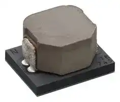
MYSGK1R830FRSR
DC/DC POL Converter, Adjustable, Buck, 4.5 V to 5.5 V in, 700mV to 1.8V out, 30A out, 42 kHz, SMD-54
⚠️ Reference pricing provided. In case of supply shortages, we will connect you with our trusted procurement partners to ensure your project's continuity.
- Manufacturer: MURATA POWER SOLUTIONS
- Product type: DC / DC Non Isolated Board Mount Converters - Adjustable Output
- SVHC: No SVHC (04-Feb-2026)
- Depth: 14mm
- Width: 11mm
- Height: 8.3mm
- Topology: Synchronous Buck (Step Down)
- No. of Pins: 54Pins
- Product Range: MonoBK MYSGK Series
- No. of Outputs: 1 Output
- Output Current: 30A
- Output Power Max: 54W
- Input Voltage Max: 5.5V
- Input Voltage Min: 4.5V
- Output Current Max: 30A
- Output Voltage Max: 1.8V
- Output Voltage Min: 700mV
- Switching Frequency: 425kHz
- Input Voltage DC Max: 15V
- Input Voltage DC Min: 4.5V
- DC / DC Converter Type: Step Down, Module
- DC / DC Converter IC Case: SMD
- Operating Temperature Max: 85°C
- Power Supply Applications: ITE & Industrial
- DC / DC Converter Output Type: Adjustable
| Delivery and price | |
|---|---|
| Units per pack | 250 |
| Price | 10.94 € |
| Current stock | 10+ |
| Lead time | 30 days |
Datasheet

**MYSGK1R830 Series**

**Mono Block Type Small & High Power Density 30A DC-DC Converter Series**

## **PRODUCT  OVERVIEW**

**Typical unit**

## **FEATURES**

■Settable output voltage from 0.7 to 1.8Vdc

■Up to 30A of output current

■Quick response to load change

■Ultra  small  surface mount package

14.0 x 11.0 x 8.3mm

■High efficiency of 89.6%

■Outstanding thermal derating performance ■Over current protection ■On/Off control (Positive logic)

The **MYSGK1R830 series** are miniature Mono Block type non-isolated Point-of-Load (PoL) DC-DC power converters for embedded applications. The tiny form factor measures only 14.0 x 11.0 x 8.3mm. Applications include powering FPGA/CPU’s, datacom/telecom systems, Distributed Bus Architectures (DBA), programmable logic and mixed voltage systems.

The converters have input voltage ranges of 4.5 to 5.5Vdc or 7.5 to 14.0Vdc and a maximum output current of 30A. Based on a fixed frequency synchronous buck converter switching topology, this high power conversion efficient PoL module features settable output voltage 0.7 to 1.8Vdc, On/Off control and Power Good signal output. These converters also include under voltage lock out (UVLO), output short circuit protection and over-current protection.

■Power Good signal

■RoHS-6 hazardous substance compliance ■High Reliability / Heat Shock Testing - 700cycle ( 40 to +125degC)

■Meets CISPR 22 class B conducted emission

## **SIMPLIFIED  APPLICATION**

MYSGK1R830 Series

MYSGK1R830FRSR MYSGK1R830ERSR Cin:47uF/10V x 2pcs Cin:22uF/25V  x 2pcs Co:220µF/4V   x 3pcs  + 100uF/6.3V   x 1pc Co:220µF/4V   x 3pcs  + 100uF/6.3V   x 1pc

(Typical topology is shown. Murata recommends an external input fuse.)

**http://www.murata.com/products/power**

Export Control Code : X0863 Document No : DC_R170013

MYSGK1R830 Series A01 Page 1 of 22

**MYSGK1R830 Series**

**Mono Block Type Small & High Power Density 30A DC-DC Converter Series**

|PART NUMBER|OUTPUT|OUTPUT|OUTPUT|OUTPUT|OUTPUT|OUTPUT|INPUT|INPUT|INPUT|INPUT|Efficiency<br>(%)|ON/OFF|PACKAGE|
|---|---|---|---|---|---|---|---|---|---|---|---|---|---|
||Vout<br>(Vdc)|Iout<br>(A, max.)|Power<br>(W)|R/N typ.<br>(% of Vout)|Regulation(max.)||Vin typ.<br>(Vdc)|Range<br>(Vdc)|Iin no load<br>(mA)|Iin full load<br>(A)|||(mm)|
||||||Line(%)|Load(%)||||||||
|MYSGK1R830FRSR|0.7-1.8<br>(typ.:1.8V)|30|54|0.4|±1.0|±1.5|5|4.5-5.5|40|12.04|89.6|Yes<br>(Positive)|14.0 x 11.0 x 8.3|
|MYSGK1R830ERSR||||0.5|±1.0|±1.5|12|7.5-14|80|5.02|88.3|||


1.All specifications are at typical line voltage, Vout = 1.8V and full load, +25degC unless otherwise noted. Output capacitors are 220uF x 3 ceramic + 100uF x 1 ceramic.

Input capacitors is 22uF x 2 ceramic or 47uF x 2 ceramic and plenty electrolytic capacitors. See detailed specifications. Input and Output capacitors are necessary for our test equipment.

2.Use adequate ground plane and copper thickness adjacent to the converter.

## **PART NUMBER STRUCTURE**

**==> picture [495 x 173] intentionally omitted <==**

**----- Start of picture text -----**<br>
MY SGK 1R8 30 E R S R<br>*<br>Murata products<br>Internal Code<br>Internal Code<br>Maximum Output Current<br>30 : 30A<br>Series Name ON/OFF Control Logic<br>S : Positive Logic<br>an Maximum  T Output Voltage 7 | " " L<br>1R8 : 1.8V<br>Input Voltage Range<br>E : 7.5-14.0V<br>F : 4.5-5.5V<br>**----- End of picture text -----**<br>


## **Product Marking**

Because of the small size of these products, the product marking contains a character-reduced code to indicate the model number and manufacturing date code. Not all items on the marking are always used. Please note that the marking differs from the product photograph. Here is the layout of the Marking.

**==> picture [212 x 73] intentionally omitted <==**

**----- Start of picture text -----**<br>
Layout(reference) Codes(reference)<br>D<br>D Factory code<br>1 F Product code<br>1 F (Please see product code table beside)<br>7 6 □<br>76□ Manufacturing date code<br>**----- End of picture text -----**<br>


|**Part Number**|**Product Code**|
|---|---|
|MYSGK1R830FRSR|1F|
|MYSGK1R830ERSR|E1|


The manufacturing date code is three characters: First character - Last digit of manufacturing Year For example "7" means "2017" Second character - Month code (1 through 9 and X through Z) For example "6" means "June" Third character - Manufacturing date code

The marking contains three rows of information:

First row - Factory code Second row - Product code

**http://www.murata.com/products/power**

MYSGK1R830 Series A01 Page 2 of 22

**MYSGK1R830 Series**

**Mono Block Type Small & High Power Density 30A DC-DC Converter Series**

|**ABSOLUTE MAXIMUM RATINGS**|**Conditions**|**Minimum**|**Typical**|**Maximum**|**Units**|
|---|---|---|---|---|---|
|Input Voltage||-0.3||6.5|Vdc|
|ON/OFF Pin|Power on, referred to -Vin|-0.3||Vin-1.5|Vdc|
|PGOOD/Trim Pins|Power on, referred to -Vin||Source ONLY|||
|Vout||0.7||2.0|Vdc|
|Output Current|Current-limited, no damage, short-circuit protected|0||30|A|
|Storage Temperature Range|Vin = Zero (no power)|-40||125|degC|
|Absolute maximums are stress ratings. Exposure of devices to greater than any of these conditions may adversely affect long-term reliability. Proper operation under conditions<br>other than those listed in the Performance/Functional Specifications Table is not implied or recommended.||||||
|**INPUT**|**Conditions**|**Minimum**|**Typical**|**Maximum**|**Units**|
|Operating Voltage Range||4.5|5|5.5|Vdc|
|Start-up Threshold|Rising input voltage||4.25||Vdc|
|Under Voltage Shutdown|Note 12||4.05||Vdc|
|Internal Filter Type|||Capacitive|||
|Input Current||||||
|Full Load Conditions|Vin = 5.0V, Vout = 1.8V, Iout = 30A||12.5||A|
|Low Line|Vin = 4.5V, Vout = 1.8V, Iout = 30A||13.5||A|
|No Load Current|Iout = 0A, unit = ON||40||mA|
|Shut-Down Mode Input Current|||2||mA|
|**GENERAL and SAFETY**|**Conditions**|**Minimum**|**Typical**|**Maximum**|**Units**|
|Efficiency|Vin = 5.0V, Vout = 1.8V, Iout = 30A||89.6||%|
||Vin = 5.0V, Vout = 1.0V, Iout = 30A||84.2|||
|Safety|Certified to UL-60950-1, CSA-C22.2 No. 60950-1,<br>IEC/EN60950-1, 2nd edition(pending)|Pending||||
|Calculated MTBF (Note 3)|+40degC, Vin = 5.0V, Vout = 1.8V, Iout = 50%||3,000,000||hours|
|**DYNAMIC CHARACTERISTICS**|**Conditions**|**Minimum**|**Typical**|**Maximum**|**Units**|
|Fixed Switching Frequency|||425||kHz|
|Startup Time (Vin ON)|Vout = 1.8V (Vin On to 90% of Vout)||4.9||ms|
|Startup Time (Remote ON)|Vout = 1.8V (Remote On to 90% of Vout)||3.9||ms|
|Dynamic Load Response|(50-100% load step, di/dt)||0.5||A/us|
|Dynamic Load Peak Deviation|same as above||±3.0%||Voset|
|**FUNCTIONS**|**Conditions**|**Minimum**|**Typical**|**Maximum**|**Units**|
|Remote On/Off Control (Note 4)||||||
|Logic||||||
|ON State Range|ON = +1.8Vmin. to +Vin-1.5Vmax. or left open|1.8||Vin-1.5|V|
|OFF State Range|OFF = -0.1V to +0.5Vmax.|-0.1||0.5|V|
|Control Current|Open collector/drain|||-|mA|
|Power-Good Output(Pulled upto 5.0Vreg(typ.)internally)||||||
|PGood TRUE(HI)||(Voset x 95%) < Vout < (Voset x 105%)|||V|
|PGood FALSE(LO)||Out of above range|||V|


**http://www.murata.com/products/power**

MYSGK1R830 Series A01 Page 3 of 22

**MYSGK1R830 Series**

**Mono Block Type Small & High Power Density 30A DC-DC Converter Series**

## **FUNCTIONAL SPECIFICATIONS OF MYSGK1R830FRSR (Note 1)**

|**OUTPUT**|**Conditions**|**Minimum**|**Typical**|**Maximum**|**Units**|
|---|---|---|---|---|---|
|Total Output Power Range|See Derating|0||54|W|
|Voltage||||||
|Output Voltage Range|Note 10|0.7||1.8|Vdc|
|Minimum Loading|||None|||
|Accuracy (50% load, untrimmed)|Vin = 5.0V, Vout = 1.8V, Cout = 760uF, Ta = 25degC|±1|||% of Vout|
|Over Voltage Protection|Note 13||120%||Vout|
|Under Voltage Protection|||68%||Vout|
|Current||||||
|Output Current Range|Note 2|0||30|A|
|Current Limit Inception|After warmup||38||A|
|Short Circuit||||||
|Short Circuit Duration (remove short for recovery)|Output shorted to ground, no damage||Continuous|||
|Short Circuit Protection Method|Note 5||Hiccup|||
|Pre-bias Start-up||Converter will start up if the external output voltage<br>is less than set Vout.||||
|Regulation (Note8)||||||
|Line Regulation|Vin = min. to max.|||±1|% of Vout|
|Ripple and Noise(20MHz bandwidth)|Note 6||10|30|mV pk-pk|
|External Output Capacitance Range(Note 11)||760||6000|uF|
|**MECHANICAL(Common)**|**Conditions**|**Minimum**|**Typical**|**Maximum**|**Units**|
|Mechanical Dimension|L x W x H|14.0(typ.) x 11.0(typ.) x 8.3(max.)|||mm|
|Weight|||4.21||grams|
|**ENVIRONMENTAL(Common)**|**Conditions**|**Minimum**|**Typical**|**Maximum**|**Units**|
|Operating Ambient Temperature Range|With Derating (Note 2,7)|-40||85|degC|
|Storage Temperature Range|Vin = Zero (no power)|-40||125|degC|
|Thermal Protection/Shutdown|Measured in module (Note9)||165||degC|
|Moisture Sensitivity Level||3||||
|RoHS Rating|||RoHS-6|||


**http://www.murata.com/products/power**

MYSGK1R830 Series A01 Page 4 of 22

**MYSGK1R830 Series**

**Mono Block Type Small & High Power Density 30A DC-DC Converter Series**

|**ABSOLUTE MAXIMUM RATINGS**|**Conditions**|**Minimum**|**Typical**|**Maximum**|**Units**|
|---|---|---|---|---|---|
|Input Voltage||-0.3||16|Vdc|
|ON/OFF Pin|Power on, referred to -Vin|-0.3||7|Vdc|
|PGOOD/Trim Pins|Power on, referred to -Vin||Source ONLY|||
|Vout||0.7||2.0|Vdc|
|Output Current|Current-limited, no damage, short-circuit protected|0||30|A|
|Storage Temperature Range|Vin = Zero (no power)|-40||125|degC|
|Absolute maximums are stress ratings. Exposure of devices to greater than any of these conditions may adversely affect long-term reliability. Proper operation under conditions<br>other than those listed in the Performance/Functional Specifications Table is not implied or recommended.||||||
|**INPUT**|**Conditions**|**Minimum**|**Typical**|**Maximum**|**Units**|
|Operating Voltage Range||7.5|12|14|Vdc|
|Start-up Threshold|Rising input voltage||5.7||Vdc|
|Under Voltage Shutdown|Note 12||4.9||Vdc|
|Internal Filter Type|||Capacitive|||
|Input Current||||||
|Full Load Conditions|Vin = 12.0V, Vout = 1.8V, Iout = 30A||5.25||A|
|Low Line|Vin = 7.5V, Vout = 1.8V, Iout = 30A||8.00||A|
|No Load Current|Iout = 0A, unit = ON||80||mA|
|Shut-Down Mode Input Current|||2||mA|
|**GENERAL and SAFETY**|**Conditions**|**Minimum**|**Typical**|**Maximum**|**Units**|
|Efficiency|Vin = 12.0V, Vout = 1.8V, Iout = 30A||88.3||%|
||Vin = 12.0V, Vout = 1.0V, Iout = 30A||83.4|||
|Safety|Certified to UL-60950-1, CSA-C22.2 No. 60950-1,<br>IEC/EN60950-1, 2nd edition(pending)|Pending||||
|Calculated MTBF (Note 3)|+40degC, Vin = 12.0V, Vo = 1.8V, Iout = 50%||1,700,000||hours|
|**DYNAMIC CHARACTERISTICS**|**Conditions**|**Minimum**|**Typical**|**Maximum**|**Units**|
|Fixed Switching Frequency|||425||kHz|
|Startup Time (Vin ON)|Vout = 1.8V (Vin On to 90% of Vout)||4.9||ms|
|Startup Time (Remote ON)|Vout = 1.8V (Remote On to 90% of Vout)||3.9||ms|
|Dynamic Load Response|(50-100% load step, di/dt)||0.5||A/us|
|Dynamic Load Peak Deviation|same as above||±3.0%||Voset|
|**FUNCTIONS**|**Conditions**|**Minimum**|**Typical**|**Maximum**|**Units**|
|Remote On/Off Control (Note 4)||||||
|Logic||||||
|ON State Range|ON = +1.8Vmin. to +5.0V max. or left open|1.8||5.0|V|
|OFF State Range|OFF = -0.1V to +0.5V.max.|-0.1||0.5|V|
|Control Current|Open collector/drain|||-|mA|
|Power-Good Output(Pulled upto 5.0Vreg(typ.)internally)||||||
|PGood TRUE(HI)||(Voset x 95%) < Vout < (Voset x 105%)||||
|PGood FALSE(LO)||Out of above range||||


**http://www.murata.com/products/power**

MYSGK1R830 Series A01 Page 5 of 22

**MYSGK1R830 Series**

**Mono Block Type Small & High Power Density 30A DC-DC Converter Series**

|**OUTPUT**|**Conditions**|**Minimum**|**Typical**|**Maximum**|**Units**|
|---|---|---|---|---|---|
|Total Output Power|See Derating|0||54|W|
|Voltage||||||
|Output Voltage Range|Note 10|0.7||1.8|Vdc|
|Minimum Loading|||None|||
|Accuracy (50% load, untrimmed)|Vin = 12.0V, Vout = 1.8V, Cout = 760uF, Ta = 25degC|±1|||% of Vout|
|Overvoltage Protection|Note 13||120%||Vout|
|Under voltage Protection|||68%||Vout|
|Current||||||
|Output Current Range|Note 2|0||30|A|
|Current Limit Inception|After warmup||40||A|
|Short Circuit||||||
|Short Circuit Duration (remove short for recovery)|Output shorted to ground, no damage||Continuous|||
|Short Circuit Protection Method|Note 5||Hiccup|||
|Pre-bias Start-up||Converter will start up if the external output voltage<br>is less than set Vout.||||
|Regulation (Note8)||||||
|Line Regulation|Vin = min. to max.|||±1|% of Vout|
|Ripple and Noise(20MHz bandwidth)|Note 6||15|30|mV pk-pk|
|External Output  Capacitance Range(Note 11)||760||6000|uF|


## **Specification Notes**

(1)Specifications are typical at +25degC, Vin=typical +5.0V(MYSGK1R830FRSR) or +12.0V(MYSGK1R830ERSR), Vout=typical (+1.8V), full load, external caps and natural convection unless otherwise indicated. All models are tested and specified with external 220uF x 3 ceramic + 100uF x 1 ceramic output capacitors, 22uF x 2 (for MYSGK1R830ERSR) or 47uF x 2 (for MYSGK1R830FRSR) ceramic and plenty electrolytic external input capacitors. All capacitors are low ESR types. These capacitors are necessary to accommodate our test equipment and may not be required to achieve specified performance in your applications. However, Murata recommends installation of these capacitors.

(2)Note that Maximum Power Derating curves indicate an average current at typical input voltage. At higher temperatures and/or no airflow, the converter will tolerate brief full current outputs if the total RMS current over time does not exceed the Derating curve.

(3)Mean Time Between Failure is calculated using the MIL-HDBK-217 Note2 method,  +40degC, half output load, natural air convection.

(4)The On/Off Control Input should use either a switch or an open collector/open drain transistor referenced to GND. A logic gate may also be used by applying appropriate external voltages which do not exceed +Vin

(5)“Hiccup” overcurrent operation repeatedly attempts to restart the converter with a brief, full-current output. If the overcurrent condition still exists, the restart current will be removed and then tried again. This short current pulse prevents overheating and damaging the converter. Once the fault is removed, the converter immediately recovers normal operation.

(6)Output noise may be further reduced by adding an external filter. At zero output current, the output may contain low frequency components which exceed the ripple specification. The output may be operated indefinitely with no load.

(7)All models are fully operational and meet published specifications, including “cold start” at -40degC.

(8)Regulation specifications describe the deviation as the line input voltage or output load current is varied from a midpoint value to either extreme.

(9)Thermal Protection/Shutdown temperature is measured with the sensor in the the converter.

(10)Do not exceed maximum power specifications when adjusting the output trim. (11)The maximum output capacitive loads depend on the Equivalent Series Resistance (ESR) of the external output capacitor and, to a lesser extent, the distance and series impedance to the load. Larger caps will reduce output noise but may change the transient response. Newer ceramic caps with very low ESR may require lower capacitor values to avoid instability. Thoroughly test your capacitors in the application.

(12)Do not allow the input voltage to degrade lower than the input under voltage shutdown voltage at all times. Otherwise, you risk having the converter turn off. The under voltage shutdown is not latching and will attempt to recover when the input is brought back into normal operating range.

(13)The outputs are intended to sink appreciable reverse current.

**http://www.murata.com/products/power**

MYSGK1R830 Series A01 Page 6 of 22

**MYSGK1R830 Series**

**Mono Block Type Small & High Power Density 30A DC-DC Converter Series**

## **Internal Circuit  Diagrams**

**ON/OFF internal circuit diagram and using guide**

**==> picture [431 x 207] intentionally omitted <==**

**----- Start of picture text -----**<br>
Vin<br>Pull UP Resistance<br>MYSGK1R830F* : 5.6kohm(±0.5%)<br>ON/OFF MYSGK1R830E* : 12kohm(±0.5%)<br>To<br>ON/OFF terminal<br>of control IC<br>Pull DOWN Resistance<br>MYSGK1R830F* : 5.6kohm(±0.5%)<br>MYSGK1R830E* : 4.7kohm(±0.5%)<br>GND<br>Recommended application<br>**----- End of picture text -----**<br>


**Power Good(P.G) internal circuit diagram and using guide**

**==> picture [360 x 222] intentionally omitted <==**

**----- Start of picture text -----**<br>
Vin<br>Regulator<br>Vout:5V typ.              Vin>5.2V<br>Vout:Vin-0.4V to Vin   Vin<5.2V<br>Source Current 100kohm(±5%)<br>0.02mA min.<br>P.G<br>P.G<br>Connect to other converter's ON/OFF  7 a Logic ControlCircuit<br>Sink Current<br>terminal etc.<br>1mA max.<br>P.G Pull-down FET<br>**----- End of picture text -----**<br>


**http://www.murata.com/products/power**

MYSGK1R830 Series A01 Page 7 of 22

**MYSGK1R830 Series**

**Mono Block Type Small & High Power Density 30A DC-DC Converter Series**

## **PERFORMANCE DATA AND OSCILLOGRAMS OF MYSGK1R830FRSR**

Efficiency vs. Line Voltage and Load Current @ +25degC (Vout = 0.7V)

On/Off Enable Delay (Vin=5.0V, Vout=0.7V, Iout=30A, Cload=760uF) Trace1=Enable, Trace2=Vout,  Trace3=P.G

**==> picture [200 x 246] intentionally omitted <==**

**----- Start of picture text -----**<br>
Vout vs. Line Voltage and Load Current @ +25degC (Vout = 0.7V)<br>Requiation<br>30.700 | de ||}<br>0.576 | | | | I o | |<br>03 6 § 2 15 18 21 244 a<br>lout [A]<br>Output Ripple and Noise<br>(Vin=5.0V, Vout=0.7V, Iout=30A, Cload=760uF, Scope BW=20MHz)<br>**----- End of picture text -----**<br>


Step Load Transient Response (Vin=5.0V, Vout=0.7V, Cload=760uF, Step Load Transient Response (Vin=5.0V, Vout=0.7V, Cload=760uF, Iout=15 to 30A, 1.0A/us) Trace 3=Vout, 50mV/div, Trace 4=Iout, 20A/div. Iout=30 to 15A, 1.0A/us) Trace 3=Vout, 50mV/div, Trace 4=Iout, 20A/div. Tek Run Sample 141 Acgs Cima) Tek Run Sample 95 Acgs Curs1 Pos Curs1 Curs2 Pos ∆V=30mV Curs2 ∆V=26mV

**http://www.murata.com/products/power**

MYSGK1R830 Series A01 Page 8 of 22

**MYSGK1R830 Series**

**Mono Block Type Small & High Power Density 30A DC-DC Converter Series**

## **PERFORMANCE DATA AND OSCILLOGRAMS OF MYSGK1R830FRSR**

Efficiency vs. Line Voltage and Load Current @ +25degC (Vout = 1.0V)

**==> picture [194 x 9] intentionally omitted <==**

**----- Start of picture text -----**<br>
Vout vs. Line Voltage and Load Current @ +25degC (Vout = 1.0V)<br>**----- End of picture text -----**<br>


On/Off Enable Delay (Vin=5.0V, Vout=1.0V, Iout=30A, Cload=760uF) Trace1=Enable, Trace2=Vout,  Trace3=P.G

Output Ripple and Noise (Vin=5.0V, Vout=1.0V, Iout=30A, Cload=760uF, Scope BW=20MHz)

Step Load Transient Response (Vin=5.0V, Vout=1.0V, Cload=760uF, Iout=15 to 30A, 1.0A/us) Trace 3=Vout, 50mV/div, Trace 4=Iout, 20A/div. Tek Run Sample 607 Acgs ∆V=38mV

Step Load Transient Response (Vin=5.0V, Vout=1.0V, Cload=760uF, Iout=30 to 15A, 1.0A/us) Trace 3=Vout, 50mV/div, Trace 4=Iout, 20A/div.

**==> picture [42 x 9] intentionally omitted <==**

**----- Start of picture text -----**<br>
∆V=40mV<br>**----- End of picture text -----**<br>


**http://www.murata.com/products/power**

MYSGK1R830 Series A01 Page 9 of 22

**MYSGK1R830 Series**

**Mono Block Type Small & High Power Density 30A DC-DC Converter Series**

## **PERFORMANCE DATA AND OSCILLOGRAMS OF MYSGK1R830FRSR**

**==> picture [457 x 246] intentionally omitted <==**

**----- Start of picture text -----**<br>
Efficiency vs. Line Voltage and Load Current @ +25degC (Vout = 1.8V) Vout vs. Line Voltage and Load Current @ +25degC (Vout = 1.8V)<br>100 Efficiency] Reguiation<br>| | | | | | | | | 1,854 H i i i i Hl |<br>95 || pt| —Vine4.5V 0 a ce oe ee<br>0 ee —Vinesv 371.500 ) a<br>Tey pp —Vine5.5V 11 a<br>C3 6 9 12 «15 18 21 24 27 «30 03 6 § 12 15 1 2 a4 of<br>lout [A] lout [A]<br>On/Off Enable Delay (Vin=5.0V, Vout=1.8V, Iout=30A, Cload=760uF) Output Ripple and Noise<br>Trace1=Enable, Trace2=Vout,  Trace3=P.G (Vin=5.0V, Vout=1.8V, Iout=30A, Cload=760uF, Scope BW=20MHz)<br>**----- End of picture text -----**<br>


On/Off Enable Delay (Vin=5.0V, Vout=1.8V, Iout=30A, Cload=760uF) Trace1=Enable, Trace2=Vout,  Trace3=P.G

Step Load Transient Response (Vin=5.0V, Vout=1.8V, Cload=760uF, Iout=15 to 30A, 1.0A/us) Trace 3=Vout, 50mV/div, Trace 4=Iout, 20A/div.

Step Load Transient Response (Vin=5.0V, Vout=1.8V, Cload=760uF, Iout=30 to 15A, 1.0A/us) Trace 3=Vout, 50mV/div, Trace 4=Iout, 20A/div.

**==> picture [42 x 9] intentionally omitted <==**

**----- Start of picture text -----**<br>
∆V=64mV<br>**----- End of picture text -----**<br>


**==> picture [42 x 9] intentionally omitted <==**

**----- Start of picture text -----**<br>
∆V=66mV<br>**----- End of picture text -----**<br>


**http://www.murata.com/products/power**

MYSGK1R830 Series A01 Page 10 of 22

**MYSGK1R830 Series**

**Mono Block Type Small & High Power Density 30A DC-DC Converter Series**

## **PERFORMANCE DATA AND OSCILLOGRAMS OF MYSGK1R830ERSR**

**==> picture [455 x 246] intentionally omitted <==**

**----- Start of picture text -----**<br>
Efficiency vs. Line Voltage and Load Current @ +25degC (Vout = 0.7V) Vout vs. Line Voltage and Load Current @ +25degC (Vout = 0.7V)<br>90 TT TTTEfficiency] | 0.721 a e ee Regulation e ee<br>60 0.679 H H H H i H H i i<br>0 3 6 9 12 1% 18 21 24 27 30 0 3 6 9 12 16 18 21 24 27 30<br>lout [Al lout[A]<br>On/Off Enable Delay (Vin=12V, Vout=0.7V, Iout=30A, Cload=760uF) Output Ripple and Noise<br>Trace1=Enable, Trace2=Vout,  Trace3=P.G (Vin=12V, Vout=0.7V, Iout=30A, Cload=760uF, Scope BW=20MHz)<br>**----- End of picture text -----**<br>


Step Load Transient Response (Vin=12.0V, Vout=0.7V, Cload=760uF, Iout=15 to 30A, 1.0A/us) Trace 3=Vout, 50mV/div, Trace 4=Iout, 20A/div.

Step Load Transient Response (Vin=12.0V, Vout=0.7V, Cload=760uF, Iout=30 to 15A, 1.0A/us) Trace 3=Vout, 50mV/div, Trace 4=Iout, 20A/div.

**==> picture [42 x 9] intentionally omitted <==**

**----- Start of picture text -----**<br>
∆V=28mV<br>**----- End of picture text -----**<br>


**==> picture [42 x 9] intentionally omitted <==**

**----- Start of picture text -----**<br>
∆V=30mV<br>**----- End of picture text -----**<br>


**http://www.murata.com/products/power**

MYSGK1R830 Series A01 Page 11 of 22

**MYSGK1R830 Series**

**Mono Block Type Small & High Power Density 30A DC-DC Converter Series**

## **PERFORMANCE DATA AND OSCILLOGRAMS OF MYSGK1R830ERSR**

Efficiency vs. Line Voltage and Load Current @ +25degC (Vout = 1.0V) Vout vs. Line Voltage and Load Current @ +25degC (Vout = 1.0V)

On/Off Enable Delay (Vin=12.0V, Vout=1.0V, Iout=30A, Cload=760uF) Trace1=Enable, Trace2=Vout,  Trace3=P.G

Output Ripple and Noise (Vin=12.0V, Vout=1.0V, Iout=30A, Cload=760uF, Scope BW=20MHz)

Step Load Transient Response (Vin=12.0V, Vout=1.0V, Cload=760uF, Step Load Transient Response (Vin=12.0V, Vout=1.0V, Cload=760uF, Iout=15 to 30A, 1.0A/us) Trace 3=Vout, 50mV/div, Trace 4=Iout, 20A/div. Iout=30 to 15A, 1.0A/us) Trace 3=Vout, 50mV/div, Trace 4=Iout, 20A/div. Tek Run Sample 40 Acgs (Ciena) Tek Run Sample 354 Acgs Curs1 Pos Curs1 ∆V=36mV Curs2 Pos ss aa pepe ∆V=38mV nega eR ES Curs2

**http://www.murata.com/products/power**

MYSGK1R830 Series A01 Page 12 of 22

**MYSGK1R830 Series**

**Mono Block Type Small & High Power Density 30A DC-DC Converter Series**

## **PERFORMANCE DATA AND OSCILLOGRAMS OF MYSGK1R830ERSR**

**==> picture [461 x 246] intentionally omitted <==**

**----- Start of picture text -----**<br>
Efficiency vs. Line Voltage and Load Current @ +25degC (Vout = 1.8V) Vout vs. Line Voltage and Load Current @ +25degC (Vout = 1.8V)<br>Efficiency Regulation<br>1<br>100 | i i i | | | i i 1.854 T T T T H T T H T<br>rf)c|i |i | | | | | | 9 | | | | | | | | |<br>oi i i i i i i i | | | | | | | | |<br>Wg pp —Vin=14V rr<br>70 H i i i | | | i i 1.748 H H i H H i H H H<br>0 3 6 9 2 15 18 21 24 27 30 0 3 6 9 12 16 18 21 24 27 30<br>lout [A] lout [A]<br>On/Off Enable Delay (Vin=12.0V, Vout=1.8V, Iout=30A, Cload=760uF) Output Ripple and Noise<br>Trace1=Enable, Trace2=Vout,  Trace3=P.G (Vin=12.0V, Vout=1.8V, Iout=30A, Cload=760uF, Scope BW=20MHz)<br>**----- End of picture text -----**<br>


Step Load Transient Response (Vin=12.0V, Vout=1.8V, Cload=760uF, Step Load Transient Response (Vin=12.0V, Vout=1.8V, Cload=760uF, Iout=15 to 30A, 1.0A/us) Trace 3=Vout, 50mV/div, Trace 4=Iout, 20A/div. Iout=30 to 15A, 1.0A/us) Trace 3=Vout, 50mV/div, Trace 4=Iout, 20A/div. Tek Run Sample 272 Acgs (wena’) Tek Run Sample 87 Acgs Curs1 Pos Curs1 ∆V=64mV Curs2 Pos Curs2 ∆V=68mV

**http://www.murata.com/products/power**

MYSGK1R830 Series A01 Page 13 of 22

**MYSGK1R830 Series**

**Mono Block Type Small & High Power Density 30A DC-DC Converter Series**

## **THERMAL DERATINGS OF MYSGK1R830FRSR & MYSGK1R830ERSR MYSGK1R830FRSR MYSGK1R830ERSR**

Maximum Current Temperature Derating at Sea Level Maximum Current Temperature Derating at Sea Level

Thermal deratings are evaluated in following condition. ・No forced air flow.

Surface(Top of the coil) temperature of the product : 105degC max

## **TRANSIENT RESPONSE DATAS OF MYSGK1R830FRSR & MYSGK1R830ERSR**

Transient response data at various conditions are showed in following table. Minimum output capacitance can serve less than 3% x Vout of deviation for 15A load change(0.5A/us).

|Part Number|Vin(V)|Vout(V)|Cout(uF)|Voltage Deviation(mV)|
|---|---|---|---|---|
|||||15-30A Load Step (0.5A/us)|
|MYSGK1R830FRSR|5|0.7|760|20|
|||1||27|
|||1.2||32|
|||1.8||45|
|MYSGK1R830ERSR|12|0.7||20|
|||1||27|
|||1.2||32|
|||1.8||46|


**http://www.murata.com/products/power**

MYSGK1R830 Series A01 Page 14 of 22

**MYSGK1R830 Series**

## **Mono Block Type Small & High Power Density 30A DC-DC Converter Series**

## **MECHANICAL SPECIFICATIONS**

## **Dimension and Pin Assignment**

**==> picture [37 x 29] intentionally omitted <==**

**----- Start of picture text -----**<br>
Unit: mm<br>Tolerances<br>± 0.25mm<br>**----- End of picture text -----**<br>


|**Pin No.**|**Function**|
|---|---|
|**1-9**|**GND**|
|**10-18**|**Vout**|
|**19**|**+Sense**|
|**20**|**Trim**|
|**21**|**-Sense**|
|**22-30**|**GND**|
|**31-39**|**Vin**|
|**40**|**ON/OFF**|
|**41**|**N.C.**|
|**42**|**Power Good**|
|**43-54**|**GND(Thermal Pad)**|


## < Bottom View >

Unit: mm

**http://www.murata.com/products/power**

MYSGK1R830 Series A01 Page 15 of 22

**MYSGK1R830 Series**

**Mono Block Type Small & High Power Density 30A DC-DC Converter Series**

## **Recommended Board Land Pattern (Top View)**

Unit: mm

## **Example of  Pattern Layout (Top View)**

**Picture**

**==> picture [37 x 7] intentionally omitted <==**

**----- Start of picture text -----**<br>
TOP VIEW<br>**----- End of picture text -----**<br>


~~——S—————~~ **24.6 x 13.0(mm)**

## **BOTTOM VIEW**

**http://www.murata.com/products/power**

MYSGK1R830 Series A01 Page 16 of 22

**MYSGK1R830 Series**

## **Mono Block Type Small & High Power Density 30A DC-DC Converter Series**

## **TAPE AND REEL INFORMATION**

**Tape Dimension**

**==> picture [27 x 7] intentionally omitted <==**

**----- Start of picture text -----**<br>
Unit: mm<br>**----- End of picture text -----**<br>


## **Reel Dimension**

**==> picture [27 x 7] intentionally omitted <==**

**----- Start of picture text -----**<br>
Unit: mm<br>**----- End of picture text -----**<br>


**http://www.murata.com/products/power**

MYSGK1R830 Series A01 Page 17 of 22

**MYSGK1R830 Series**

**Mono Block Type Small & High Power Density 30A DC-DC Converter Series**

## **TAPE SPECIFICATION**

## **Note**

1. The adhesive strength of the protective tape must be within 0.1-1.3N.

- 2.Each reel contains 150 pcs.

- 3.Each reel set in moisture-proof packaging because of MSL 3.

- 4.No vacant pocket in “Module on tape” section.

- 5.The reel is labeled with Murata part number and quantity.

- 6.The color of reel is not specified.

**http://www.murata.com/products/power**

MYSGK1R830 Series A01 Page 18 of 22

**MYSGK1R830 Series**

**Mono Block Type Small & High Power Density 30A DC-DC Converter Series**

## **TECHNICAL NOTES**

## **Input Fuse**

Certain applications and/or safety agencies may require fuses at the inputs of power conversion components. Fuses should also be used when there is the possibility of sustained input voltage reversal which is not current limited. For greatest safety, we recommend a fast blow fuse installed in the ungrounded input supply line. The installer must observe all relevant safety standards and regulations. For safety agency approvals, install the converter in compliance with the end-user safety standard.

## **Input Under-Voltage Shutdown and Start-Up Threshold**

Under normal start-up conditions, converters will not begin to regulate properly until the ramping-up input voltage exceeds and remains at the Start-Up Threshold Voltage (see Specifications). Once operating, converters will not turn off until the input voltage drops below the Under-Voltage Shutdown Limit. Subsequent restart will not occur until the input voltage rises again above the Start-Up Threshold. This built-in hysteresis prevents any unstable on/off operation at a single input voltage.

Users should be aware however of input sources near the UnderVoltage Shutdown whose voltage decays as input current is consumed (such as capacitor inputs), the converter shuts off and then restarts as the external capacitor recharges. Such situations could oscillate. To prevent this, make sure the operating input voltage is well above the UV Shutdown voltage at all times.

## **Start-Up Time**

Assuming that the output current is set at the rated maximum, the Vin to Vout Start-Up Time (see Specifications) is the time interval between the point when the ramping input voltage crosses the Start-Up Threshold and the fully loaded regulated output voltage enters and remains within its specified accuracy band. Actual measured times will vary with input source impedance, external input capacitance, input voltage slew rate and final value of the input voltage as it appears at the converter.

These converters include a soft start circuit to moderate the duty cycle of its PWM controller at power up, thereby limiting the input inrush current.

The On/Off Remote Control interval from On command to Vout regulated assumes that the converter already has its input voltage stabilized above the Start-Up Threshold before the On command. The interval is measured from the On command until the output enters and remains within its specified accuracy band. The specification assumes that the output is fully loaded at maximum rated current. Similar conditions apply to the On to Vout regulated specification such as external load capacitance and soft start circuitry.

## **Recommended Input Filtering**

The user must assure that the input source has low AC impedance to provide dynamic stability and that the input supply has little or no inductive content, including long distributed wiring to a remote power supply. For best performance, we recommend installing a low-ESR capacitor immediately adjacent to the converter’s input terminals.

The capacitor should be a ceramic type such as the Murata GRM32 series and a electrolytic type such as Panasonic OSCON series.

Initial suggested capacitor values are 22uF x 2 or 47uF x 2 ceramic type and 1000uF x 1 electrolytic type , rated at twice the expected maximum input voltage. Make sure that the input terminals do not go below the under voltage shutdown voltage at all times. More input bulk capacitance may be added in parallel (either electrolytic or tantalum) if needed.

## **Recommended Output Filtering**

The converter will achieve its rated output ripple and noise with additional external capacitor. The user may install more external output capacitance reduce the ripple even further or for improved dynamic response. Again, use low-ESR ceramic (Murata GRM32 series). Initial values of 220uF x 3 ceramic type + 100uF x 1 ceramic type may be tried, either single or multiple capacitors in parallel. Mount these close to the converter. Measure the output ripple under your load conditions. Use only as much capacitance as required to achieve your ripple and noise objectives. Excessive capacitance can make step load recovery sluggish or possibly introduce instability. Do not exceed the maximum rated output capacitance listed in the specifications.

## **Output Noise**

All models in this converter series are tested and specified for output noise using designated external input/output components, circuits and layout as shown in the figures below. In the figure below, the two copper strips simulate real-world printed circuit impedances between the power supply and its load. In order to minimize circuit errors and standardize tests between units, scope measurements should be made using BNC connectors or the probe ground should not exceed one half inch and soldered directly to the test circuit.

**==> picture [207 x 113] intentionally omitted <==**

**----- Start of picture text -----**<br>
COPPER STRIP<br>VOUT<br>C1 C2 SCOPE RLOAD<br>GND<br>COPPER<br>STRIP<br>3-7mm<br>C1=220uF x 3 CERAMIC + 100uF x 1 CERAMIC<br>C2=OPEN<br>**----- End of picture text -----**<br>


Figure :Measuring Output Ripple and Noise

## **Minimum Output Loading Requirements**

All models regulate within specification and are stable under no load to full load conditions. Operation under no load might however slightly increase output ripple and noise.

## **Thermal Shutdown**

To prevent many over temperature problems and damage, these converters include thermal shutdown circuitry. If environmental conditions cause the temperature of the converter’s to rise above the Operating Temperature Range up to the shutdown temperature, an on-board electronic temperature sensor will power down the unit. When the temperature decreases below the turn-on threshold, the converter will automatically restart.

**http://www.murata.com/products/power**

MYSGK1R830 Series A01 Page 19 of 22

**MYSGK1R830 Series**

**Mono Block Type Small & High Power Density 30A DC-DC Converter Series**

**CAUTION:** If you operate too close to the thermal limits, the

converter may shut down suddenly without warning. Be sure to thoroughly you’re your application to avoid unplanned thermal shutdown.

## **Temperature Derating Curves**

The graphs in this data sheet illustrate typical operation under a variety of conditions. The derating curves show the maximum continuous ambient air temperature. Note that these are AVERAGE measurements.

Note that the temperatures are of the ambient airflow, not the converter itself which is obviously running at higher temperature than the outside air. Also note that very low flow rates (below about 25 LFM) are similar to “natural convection,” that is, not using fan-forced airflow. Murata makes Characterization measurements in a closed cycle wind tunnel with calibrated airflow. We use both thermocouples and an infrared camera system to observe thermal performance. **CAUTION:** These graphs are all collected at slightly above Sea Level altitude. Be sure to reduce the derating for higher density altitude.

## **Output Current Limiting**

Current limiting inception is defined as the point at which full power falls below the rated tolerance. See the Performance/Functional Specifications. Note particularly that the output current may briefly rise above its rated value in normal operation as long as the average output power is not exceeded. This enhances reliability and continued operation of your application. If the output current is too high, the converter will enter the short circuit condition. **Output Short Circuit Condition**

When a converter is in current-limit mode, the output voltage will drop as the output current demand increases. Following a time-out period, the converter will restart, causing the output voltage to begin ramping up to its appropriate value. If the short-circuit condition persists, another shutdown cycle will initiate. This rapid on/off cycling is called “hiccup mode”. The hiccup cycling reduces the average output current, thereby preventing excessive internal temperatures and/or component damage. A short circuit can be tolerated indefinitely.

The “hiccup” system differs from older latching short circuit systems because you do not have to power down the converter to make it restart. The system will automatically restore operation as soon as the short circuit condition is removed.

## **UVP/OVP Function**

This product monitors a feedback voltage to detect over and under voltage. When the feedback voltage becomes lower than 68% of the target voltage, after 1ms, the product latches OFF. This function is enables after softstart is complete.

When the feedback voltage becomes higher than 120% of the target voltage, the circuit operates sink-mode to decrease output voltage until reaching a negative current limit (-38A typ.). Upon reaching the negative current limit, sink-mode is turned off and the device restarts for a short time. The device operates in this cycle until the output voltage is pulled down under the UVP threshold voltage for 1ms. After the 1ms, the circuit latches into sink-mode. The fault is cleared with a reset of Vin or by retoggling the ON/OFF pin.

## **Remote On/Off Control**

Please refer to the Connection Diagram on page 1 for On/Off connections.

Positive logic models are enabled when the On/Off pin is left open or is pulled high to Vin with respect to GND. An internal bias current causes the open pin to rise to Vin. Positive-polarity devices are disabled when the On/Off is grounded or brought to within a low voltage (see Specifications) with respect to GND.

Dynamic control of the On/Off function should be able to sink appropriate signal current when brought low and withstand appropriate voltage when brought high. Be aware too that there is a finite time in milliseconds (see Specifications) between the time of On/Off Control activation and stable, regulated output. This time will vary slightly with output load type and current and input conditions.

## **Output Capacitive Load**

Users should only consider adding capacitance to reduce switching noise and/or to handle spike current load steps. Install only enough capacitance to achieve noise objectives. Excess external capacitance may cause regulation problems, degraded transient response and possible oscillation or instability.

## **Soldering Guidelines**

Murata recommends the specifications below when installing these converters. These specifications vary depending on the solder type.

Exceeding these specifications may cause damage to the product. Your production environment may differ therefore please thoroughly review these guidelines with your process engineers.

**http://www.murata.com/products/power**

MYSGK1R830 Series A01 Page 20 of 22

**MYSGK1R830 Series**

**Mono Block Type Small & High Power Density 30A DC-DC Converter Series**

|**Reflow Solder Operations for surface-mountproducts**|**Reflow Solder Operations for surface-mountproducts**|
|---|---|
|For Sn/Ag/Cu based solders:||
|Preheat Temperature|Less than 1degCper second|
|Time over Liquidus|45 to 75 seconds|
|Maximum Peak Temperature|250degC|
|CoolingRate|Less than 3degCper second|
|For Sn/Pb based solders:||
|Preheat Temperature|Less than 1degCper second|
|Time over Liquidus|60 to 75 seconds|
|Maximum Peak Temperature|235degC|
|CoolingRate|Less than 3degCper second|


## **Recommended Lead-free Solder Reflow Profile**

## **Output Voltage Adjustment**

The output voltage may be adjusted over a limited range by connecting an external trim resistor (Rtrim) between the Trim pin and GND pin. The Rtrim resistor must be a 1/10W precision metal film type, ±0.5% accuracy or better with low temperature coefficient, ±100ppm/degC or better. Mount the resistor close to the converter with very short leads or use a surface mount trim resistor.

In the table below, the estimated resistance is given at limited condition ; Vin : typ., Ta : 25degC, Iout : max., Cout : 760uF. (Please look at Test Circuit which is shown below). Do not exceed the specified limits of the output voltage or the converter’s maximum power rating when applying these resistors. Also, avoid high noise at the Trim input. However, to prevent instability, you should never connect any capacitors between Trim pin and GND pin.

|**Output Voltage**|**Estimated Rtrim (kohm)**<br>**MYSGK1R830 Series**|
|---|---|
|0.7V|56 + 3.6|
|1.0V|15|
|1.2V|10|
|1.5V|6.2 + 0.47|
|1.8V|3.0 + 2.0|


**CAUTION: Do not reflow the converter as follows, because the converter may fall from the substrate during reflowing.**

**Mother Substrate Converter**

## **Pb-free solder processes**

For Pb-free solder processes, the product is qualified for MSL 3 according to IPC/JEDEC standard J-STD-020D. During reflow PRODUCT must not exceed 250degC at any time.

## **Dry Pack Information**

## **Resistor Trim Equation**

MYSGK1R830 Series

5.996 Rtrim ( kohm ) = ( Vout - 0.5996 )

Output voltage depends on the value of capacitance of Cout in this product , the smaller Cout may cause the higher output voltage. The equations above are only reference, so please check output voltage and adjust Rtrim in user circumstances. To increase(decrease) output voltage is obtained by decreasing(increasing) value of Rtrim .

Products intended for Pb-free reflow soldering processes are delivered in standard moisture barrier bags according to IPC/JEDEC standard J-STD-033.

(Handling, packing, shipping and use of moisture/reflow sensitivity surface mount devices.)

Using products in high temperature Pb-free soldering processes requires dry pack storage and handling. In case the products have been stored in an uncontrolled environment and no longer can be considered dry, the modules must be baked according to J-STD-033.

**http://www.murata.com/products/power**

MYSGK1R830 Series A01 Page 21 of 22

**MYSGK1R830 Series**

# **Mono Block Type Small & High Power Density 30A DC-DC Converter Series**

## **APPENDIX**

## **Test Circuit**

Vin:DC Power Supply

RL:Electronic Load Device

For MYSGK1R830FRSR

C1:1000uF/25V x 1pc Electrolysis Capacitor C2:47uF/10V x 2pcs (GRM32ER71A476KE15:Murata)

C3:220uF/4V x 3pcs (GRM32EC80G227ME05:Murata)

+ 100uF/6.3V x 1pc (GRM32EC80J107ME20L:Murata)

For MYSGK1R830ERSR

C1:1000uF/25V x 1pc Electrolysis Capacitor

C2:22uF/25V x 2pcs (GRM32ER71E226KE15:Murata) C3:220uF/4V x 3pcs (GRM32EC80G227ME05:Murata) + 100uF/6.3V x 1pc (GRM32EC80J107ME20L:Murata)

*Do not connect any additional components between the Trim pin and Vout or between the Trim and Sense pins. Use only the specified connections.

**http://www.murata.com/products/power**

Specifications are subject to change without notice.

MYSGK1R830 Series A01 Page 22 of 22
Updated at April 10, 2026
About Novapart
Novapart is a B2B electronic component broker specialising in stock shortages and cost reduction. We source hard-to-find parts and identify compliant alternatives across a catalogue of 410,000+ components from 500+ manufacturers.
Learn more →Stock Shortage Specialist
When a component is unavailable, discontinued or has an unacceptable lead time, we tap into our network of vetted European and Asian distributors to source what you need — without compromising on quality or traceability.
Request a quote →Compliant Alternatives
We identify pin-to-pin, electrically equivalent substitutes that meet the same certifications (RoHS, AEC-Q100, REACH) as your original specification — validated against datasheets, not just part numbers. Often at a lower cost.
BOM Analysis service →