
Image not available
Illustrative purposes only

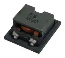
MYSGK02506BRSR
DC/DC POL Converter, Adjustable, Buck, 13.5 V to 42 V in, 5V to 25 V out, 6 A out, 380 kHz, SMD-37
⚠️ Reference pricing provided. In case of supply shortages, we will connect you with our trusted procurement partners to ensure your project's continuity.
- Manufacturer: MURATA POWER SOLUTIONS
- Product type: DC / DC Non Isolated Board Mount Converters - Adjustable Output
- SVHC: No SVHC (04-Feb-2026)
- Depth: 14.7mm
- Width: 16.3mm
- Height: 7.5mm
- Topology: Synchronous Buck (Step Down)
- No. of Pins: 37Pins
- Product Range: MonoBK MYSGK Series
- No. of Outputs: 1 Output
- Output Current: 6A
- Output Power Max: 150W
- Input Voltage Max: 42V
- Input Voltage Min: 13.5V
- Output Current Max: 6A
- Output Voltage Max: 25V
- Output Voltage Min: 5V
- Switching Frequency: 380kHz
- Input Voltage DC Max: 42V
- Input Voltage DC Min: 9.6V
- DC / DC Converter Type: Step Down, Module
- DC / DC Converter IC Case: SMD
- Operating Temperature Max: 85°C
- Power Supply Applications: ITE & Industrial
- DC / DC Converter Output Type: Adjustable
| Delivery and price | |
|---|---|
| Units per pack | 250 |
| Price | 8.36 € |
| Current stock | 500+ |
| Lead time | 30 days |
Datasheet

## **MYSGK02506BRSR** ~~ees~~ DC-DC converter
## **Typical unit**
## **FEATURES**
Input Voltage range 13.5 to 42Vdc
(Absolute maximum input voltage:50Vdc)
Settable output voltage range 5 to 25Vdc
Up to 6A of output current
Ultra small surface mount package
14.7 x 16.3 x 7.5mm
High efficiency `:` 98%(at Vo=24Vdc)
Outstanding thermal derating performance
Short Circuit Protection
Programmable UVLO
On/Off control (Positive logic)
## **PRODUCT OVERVIEW**
The MYSGK02506BRSR is miniature Solid Block type nonisolated DC-DC power converter for embedded applications. The tiny form factor measures only 14.7 x 16.3 x 7.5 mm. The converter have input voltage ranges of 13.5 to 42Vdc and a maximum output current of 6A. Based on a fixed frequency synchronous buck converter switching topology, this high power conversion efficient module features settable output voltage 5 to 25Vdc and On/Off control.
This converter also include under voltage lock out (UVLO) and output short circuit protection.
Operating Temperature range -40 to +85 degC
## **TYPICAL APPLICATION**
**==> picture [372 x 146] intentionally omitted <==**
**----- Start of picture text -----**<br>
Vin Vin Vo Vo<br>RUVLO1<br>EN/ +<br>UVLO VAR C11 C12<br>C1 C2 C3 C4<br>RUVLO2 GND RVER<br>C1-4,C11 : Ceramic capacitor 4.7uF/50V(GRM31CR71H475KA12L:MURATA)<br>C12 : Conductive Polymer Hybrid Aluminum Electrolytic Capacitor 68uF/35V<br>(HHXB350ARA680MF80G φ6.3×L7.7:NIPPON CHEMI-CON)<br>**----- End of picture text -----**<br>
**http://www.murata.com/products/power**
Export Control Code : X0863
MYSGK02506BRSR A04 Page 1 of 18
**MYSGK02506BRSR**
DC-DC converter
PERFORMANCE SPECIFICATIONS SUMMARY AND ORDERING GUIDE Output Input Efficiency Package Model Number Vo Io Power R/N Max. Regulation (Max.) Vin typ. Range Iin, no load Iin, full load (%) (mm) (Vdc) (A,Max.) (W) (mV p-p) (Vdc) (Vdc) Typ.(mA) Typ.(A) Line (%) Load (%) 5-25 MYSGK02506BRSR 6 150 50 ±2.0 ±2.0 36 13.5-42 22 4.06 98 14.7 x 16.3 x 7.5 (typ.:24V) ~~Sr~~ 1.All specifications are at typical line voltage, Vo = typ. and full load, +25degC unless otherwise noted. Output capacitors are 4.7uF ceramic and 68uF conductive polymer hybrid aluminum electrolytic capacitor. Input capacitors is 4.7uFx 4 ceramic and plenty electrolytic capacitors. See detailed specifications. Input and output capacitors are necessary for our test equipment.
2.Use adequate ground plane and copper thickness adjacent to the converter.
## PART NUMBER STRUCTURE
**==> picture [320 x 150] intentionally omitted <==**
**----- Start of picture text -----**<br>
MY SGK 025 06 BRSR<br>Murata products Internal Code<br>Series Name Maximum Output Current<br>06 = 6A<br>Maximum Output Voltage<br>025 = 25V<br>**----- End of picture text -----**<br>
## **PRODUCT MARKING**
Codes
**==> picture [395 x 181] intentionally omitted <==**
**----- Start of picture text -----**<br>
Layout Codes<br>□□□□□□□□****** Item Contents<br>□□□□□□□□ Lot No. (8-digit alphanumeric)<br>EB EB Product Code<br>### = # # # Internal code<br>1pin<br>**----- End of picture text -----**<br>
**http://www.murata.com/products/power**
MYSGK02506BRSR A04 Page 2 of 18
**MYSGK02506BRSR**
DC-DC converter
## **FUNCTIONAL SPECIFICATIONS**
|**ABSOLUTE MAXIMUM RATINGS**|**Conditions**|**Minimum**|**Typical / Nominal**|**Maximum**|**Units**|
|---|---|---|---|---|---|
|**Input Voltage, Continuous**||-0.3||50|Vdc|
|**EN/UVLO**||-0.3||8.8|Vdc|
|**VARpin**|||Source ONLY|||
|**Storage Temperature Range**|Vin = Zero(nopower)|-40||125|degC|
|Absolute maximums are stress ratings. Exposure of devices to greater than any of these conditions may adversely affect long-term reliability. Proper operation under conditions other<br>than those listed in the Performance/Functional Specifications Table is not implied or recommended.||||||
|**INPUT**|**Conditions**|**Minimum**|**Typical / Nominal**|**Maximum**|**Units**|
|**Operating Voltage Range (Vin)**|Vin>Vo * 1.17|13.5|36|42|Vdc|
|**Startup threshold**|Rising input voltage<br>RUVLO1=OPEN, RUVLO2=OPEN||8.82||Vdc|
|**Shutdown threshold**|Shutdown input voltage<br>RUVLO1=OPEN, RUVLO2=OPEN||4.42||Vdc|
|**Input current**||||||
|**Full Load Conditions**|Vin = 36V,Vo = 24V,Io =6A||4.06||A|
|**No Load Current**|Vin = 36V,Vo = 24V,Io = 0A||22||mA|
|**EN/UVLO pin Voltage**|Power ON|1||8|Vdc|
|||OPEN||||
||Power OFF|-0.3||0.1|Vdc|
|**GENERAL**|**Conditions**|**Minimum**|**Typical / Nominal**|**Maximum**|**Units**|
|**Efficiency**|Vin = 36V,Vo = 24V,Io = 6A||98||%|
|**DYNAMIC CHARACTERISTICS**|**Conditions**|**Minimum**|**Typical / Nominal**|**Maximum**|**Units**|
|**Fixed Switching Frequency**|||380||kHz|
|**Startup Time(Vin ON)**|||24||ms|
|**Startup Time(EN ON)**|||24||ms|
|**OUTPUT**|**Conditions**|**Minimum**|**Typical / Nominal**|**Maximum**|**Units**|
|**Voltage**||||||
|**Output Voltage (Vo)**|RVER = 0Ω|24.12|25|25.88|Vdc|
||RVER = 86.7Ω|23.16|24|24.84|Vdc|
||RVER = 888Ω|17.37|18|18.63|Vdc|
||RVER = 1.65kΩ|14.47|15|15.53|Vdc|
||RVER = 3.068kΩ|11.58|12|12.42|Vdc|
||RVER = OPEN|4.82|5|5.18|Vdc|
|**Current**||||||
|**Output Current Range (Io)**|Vin > 36V and Vo > 15.53V|0||5|A|
||Vin≦36V or Vo≦15.53V|0||6|A|
|**Short circuitprotection method**|Hiccupcurrent limiting||Non-latching|||
|**Ripple Voltage**|Vin = 36V, Vo = 24V, Io = 6A<br>20 MHz BW||50||mV p-p|
|**External Output Capacitive**||60||150|uF|
|**MECHANICAL**|**Conditions**|**Minimum**|**Typical / Nominal**|**Maximum**|**Units**|
|**Outline Dimensions**||14.7(typ.)x 16.3(typ.)x 7.5(max.)|||mm|
|**Weight**|||3.7||grams|
|**ENVIRONMENTAL**|**Conditions**|**Minimum**|**Typical / Nominal**|**Maximum**|**Units**|
|**Operating Ambient Temperature Range **||-40||85|degC|
|**Moisture Sensitivity Level**||3||||
(1)All models are tested and specified with external 4.7uF ceramic and Conductive Polymer Hybrid Aluminum Electrolytic Capacitor 68uF output capacitors and 4.7uFx4 ceramic and plenty electrolytic external input capacitors. All capacitors are low ESR types. These capacitors are necessary to accommodate our test equipment and may not be required to achieve specified performance in your applications. However, Murata recommends installation of these capacitors.
(2)Note that Maximum Power Derating curves indicate an average current at typical input voltage. At higher temperatures and/or no airflow, the converter will tolerate brief full current outputs if the total RMS current over time does not exceed the Derating curve.
(3)The On/Off Control Input should use either a switch or an open collector/open drain transistor referenced to GND. A logic gate may also be used by applying appropriate external voltages which do not exceed +8V. (4)“Hiccup” operation repeatedly attempts to restart the converter with a brief, full-current output. If the short circuit condition still exists, the restart current will be removed and then tried again.
This short current pulse prevents overheating and damaging the converter. Once the fault is removed, the converter immediately recovers normal operation.
(5)Do not exceed maximum power specifications when adjusting the output trim.
(6)The maximum output capacitive loads depend on the Equivalent Series Resistance (ESR) of the external output capacitor and, to a lesser extent, the distance and series impedance to the load. Larger capacitors will reduce output noise but may change the transient response. Newer ceramic capacitors with very low ESR may require lower capacitor values to avoid instability. Thoroughly test your capacitors in the application. Please refer to the Output Capacitive Load Application Note.
(7)Do not allow the input voltage to degrade lower than the input under voltage shutdown voltage at all times. Otherwise, you risk having the converter turn off. The under voltage shutdown is not latching and will attempt to recover when the input is brought back into normal operating range.
**http://www.murata.com/products/power**
MYSGK02506BRSR A04 Page 3 of 18
**MYSGK02506BRSR**
DC-DC converter
**==> picture [444 x 219] intentionally omitted <==**
**----- Start of picture text -----**<br>
PERFORMANCE DATA AND OSCILLOGRAMS OF MYSGK02506BRSR<br>Efficiency vs. Line Voltage and Load Current @ +25degC. (Vo = 25V) Vo vs. Line Voltage and Load Current @ +25degC. (Vo = 25V)<br>Regulation Efficiency<br>25.87 100<br>25.58<br>96<br>25.29<br>| | | | | 92 se<br>25.00<br>es ee ee 88 | es Vin=29.2V ae<br>24.71 Vin=29.2V Vin=30V<br>24.42 Vin=30VVin=36V 84 Vin=36V<br>Vin=42V Vin=42V<br>24.13 80<br>0 1 2 3 4 5 6 0 1 2 3 4 5 6<br>Io [A] Io [A]<br>On/Off Enable Delay (Vin=36V, Vo=25V, Io=6A)Trace1=Enable, Trace2=Vo, 10ms/div Output Ripple and Noise (Vin=36V, Vo=25V, Io=6A, Scope BW=20MHz)<br>Efficiency [%]<br>Vo [V]<br>**----- End of picture text -----**<br>
**==> picture [186 x 7] intentionally omitted <==**
**----- Start of picture text -----**<br>
Output Ripple and Noise (Vin=36V, Vo=25V, Io=6A, Scope BW=20MHz)<br>**----- End of picture text -----**<br>
Step Load Transient Response (Vin=36V, Vo=25V, Io=3A to 6A, 2.5A/us) Step Load Transient Response (Vin=36V, Vo=25V, Io=3A to 6A, 2.5A/us) Trace 3=Vo, 200mV/div, Trace 4=Io, 5A/div. Trace 3=Vo, 200mV/div, Trace 4=Io, 5A/div.
**http://www.murata.com/products/power**
MYSGK02506BRSR A04 Page 4 of 18
**MYSGK02506BRSR**
## DC-DC converter
**==> picture [443 x 183] intentionally omitted <==**
**----- Start of picture text -----**<br>
PERFORMANCE DATA AND OSCILLOGRAMS OF MYSGK02506BRSR<br>Efficiency vs. Line Voltage and Load Current @ +25degC. (Vo = 24V) Vo vs. Line Voltage and Load Current @ +25degC. (Vo = 24V)<br>Regulation Efficiency<br>24.84 100<br>24.56<br>96<br>24.28<br>92<br>24.00 | i i i i | i | | |<br>88 Vin=28V<br>23.72 Vin=28V Vin=30V<br>23.44 Vin=30VVin=36V 84 Vin=36V<br>Vin=42V Vin=42V<br>23.16 80<br>0 1 2 3 4 5 6 0 1 2 3 4 5 6<br>Io [A] Io [A]<br>Vo [V]<br>Efficiency [%]<br>**----- End of picture text -----**<br>
On/Off Enable Delay (Vin=36V, Vo=24V, Io=6A)Trace1=Enable, Trace2=Vo, 10ms/div
**==> picture [186 x 7] intentionally omitted <==**
**----- Start of picture text -----**<br>
Output Ripple and Noise (Vin=36V, Vo=24V, Io=6A, Scope BW=20MHz)<br>**----- End of picture text -----**<br>
Step Load Transient Response (Vin=36V, Vo=24V, Io=3A to 6A, 2.5A/us) Trace 3=Vo, 200mV/div, Trace 4=Io, 5A/div.
Step Load Transient Response (Vin=36V, Vo=24V, Io=3A to 6A, 2.5A/us) Trace 3=Vo, 200mV/div, Trace 4=Io, 5A/div.
**http://www.murata.com/products/power**
MYSGK02506BRSR A04 Page 5 of 18
**MYSGK02506BRSR**
## DC-DC converter
## PERFORMANCE DATA AND OSCILLOGRAMS OF MYSGK02506BRSR
**==> picture [433 x 172] intentionally omitted <==**
**----- Start of picture text -----**<br>
Efficiency vs. Line Voltage and Load Current @ +25degC. (Vo = 18V) Vo vs. Line Voltage and Load Current @ +25degC. (Vo = 18V)<br>Regulation Efficiency<br>18.63 100<br>18.42<br>96<br>18.21<br>92<br>18.00<br>88 Vin=21V<br>17.79 Vin=21V<br>Vin=24V<br>17.58 Vin=24VVin=36V 84 Vin=36V<br>Vin=42V o e Vin=42V<br>17.37 80<br>0 1 2 3 4 5 6 0 1 2 3 4 5 6<br>Io [A] Io [A]<br>Efficiency [%]<br>Vo [V]<br>**----- End of picture text -----**<br>
**==> picture [442 x 7] intentionally omitted <==**
**----- Start of picture text -----**<br>
On/Off Enable Delay (Vin=36V, Vo=18V, Io=6A)Trace1=Enable, Trace2=Vo, 10ms/div Output Ripple and Noise (Vin=36V, Vo=18V, Io=6A, Scope BW=20MHz)<br>**----- End of picture text -----**<br>
**==> picture [191 x 16] intentionally omitted <==**
**----- Start of picture text -----**<br>
Step Load Transient Response (Vin=36V, Vo=18V, Io=3A to 6A, 2.5A/us)<br>Trace 3=Vo, 200mV/div, Trace 4=Io, 5A/div.<br>**----- End of picture text -----**<br>
**==> picture [190 x 16] intentionally omitted <==**
**----- Start of picture text -----**<br>
Step Load Transient Response (Vin=36V, Vo=18V, Io=3A to 6A, 2.5A/us)<br>Trace 3=Vo, 200mV/div, Trace 4=Io, 5A/div.<br>**----- End of picture text -----**<br>
**http://www.murata.com/products/power**
MYSGK02506BRSR A04 Page 6 of 18
**MYSGK02506BRSR**
## DC-DC converter
## PERFORMANCE DATA AND OSCILLOGRAMS OF MYSGK02506BRSR
**==> picture [490 x 206] intentionally omitted <==**
**----- Start of picture text -----**<br>
Efficiency vs. Line Voltage and Load Current @ +25degC. (Vo = 15V) Vo vs. Line Voltage and Load Current @ +25degC. (Vo = 15V)<br>Regulation Efficiency<br>15.51 100<br>15.34<br>96<br>15.17<br>92<br>15.00 lii||<br>88 Vin=17.5V<br>14.83 Vin=17.5V Vin=24V<br>14.66 Vin=24VVin=36V 84 Vin=36V<br>Vin=42V Vin=42V<br>14.49 80 tH E |<br>0 1 2 3 4 5 6 0 1 2 3 4 5 6<br>Io [A] Io [A]<br>On/Off Enable Delay (Vin=36V, Vo=15V, Io=6A)Trace1=Enable, Trace2=Vo, 10ms/div Output Ripple and Noise (Vin=36V, Vo=15V, Io=6A, Scope BW=20MHz)<br>Vo [V]<br>Efficiency [%]<br>**----- End of picture text -----**<br>
**==> picture [429 x 16] intentionally omitted <==**
**----- Start of picture text -----**<br>
Step Load Transient Response (Vin=36V, Vo=15V, Io=3A to 6A, 2.5A/us) Step Load Transient Response (Vin=36V, Vo=15V, Io=3A to 6A, 2.5A/us)<br>Trace 3=Vo, 200mV/div, Trace 4=Io, 5A/div. Trace 3=Vo, 200mV/div, Trace 4=Io, 5A/div.<br>**----- End of picture text -----**<br>
**http://www.murata.com/products/power**
MYSGK02506BRSR A04 Page 7 of 18
**MYSGK02506BRSR**
## DC-DC converter
## PERFORMANCE DATA AND OSCILLOGRAMS OF MYSGK02506BRSR
**==> picture [473 x 206] intentionally omitted <==**
**----- Start of picture text -----**<br>
Efficiency vs. Line Voltage and Load Current @ +25degC. (Vo = 12V) Vo vs. Line Voltage and Load Current @ +25degC. (Vo = 12V)<br>Regulation Efficiency<br>12.42 100<br>12.28<br>96<br>12.14 i|/i/ 92<br>12.00<br>— 88 | i | i Vin=14V i<br>11.86 Vin=14V Vin=24V<br>11.72 | | | | Vin=24VVin=36V | 84 | nt nnn ne ne Vin=36V 7<br>Vin=42V Vin=42V<br>11.58 80 :H J<br>0 1 2 3 4 5 6 0 1 2 3 4 5 6<br>Io [A] Io [A]<br>On/Off Enable Delay (Vin=36V, Vo=12V, Io=6A)Trace1=Enable, Trace2=Vo, 10ms/div Output Ripple and Noise (Vin=36V, Vo=12V, Io=6A, Scope BW=20MHz)<br>Vo [V]<br>Efficiency [%]<br>**----- End of picture text -----**<br>
On/Off Enable Delay (Vin=36V, Vo=12V, Io=6A)Trace1=Enable, Trace2=Vo, 10ms/div
Step Load Transient Response (Vin=36V, Vo=12V, Io=3A to 6A, 2.5A/us) Trace 3=Vo, 200mV/div, Trace 4=Io, 5A/div.
**==> picture [190 x 16] intentionally omitted <==**
**----- Start of picture text -----**<br>
Step Load Transient Response (Vin=36V, Vo=12V, Io=3A to 6A, 2.5A/us)<br>Trace 3=Vo, 200mV/div, Trace 4=Io, 5A/div.<br>**----- End of picture text -----**<br>
**http://www.murata.com/products/power**
MYSGK02506BRSR A04 Page 8 of 18
**MYSGK02506BRSR**
## DC-DC converter
## PERFORMANCE DATA AND OSCILLOGRAMS OF MYSGK02506BRSR
**==> picture [485 x 169] intentionally omitted <==**
**----- Start of picture text -----**<br>
Efficiency vs. Line Voltage and Load Current @ +25degC. (Vo = 5V) Vo vs. Line Voltage and Load Current @ +25degC. (Vo = 5V)<br>Regulation Efficiency<br>5.18 100<br>5.12 95<br>5.06 i||| 90<br>5.00 ii i i | 85 /<br>Vin=13.5V<br>4.94 Vin=13.5V 80 Vin=24V<br>Vin=24V<br>4.88 Vin=36V 75 Vin=36V<br>Vin=42V Vin=42V<br>4.82 70<br>0 1 2 3 4 5 6 0 1 2 3 4 5 6<br>Io [A] Io [A]<br>Efficiency [%]<br>Vo [V]<br>**----- End of picture text -----**<br>
On/Off Enable Delay (Vin=36V, Vo=5V, Io=6A)Trace1=Enable, Trace2=Vo, 10ms/div
Output Ripple and Noise (Vin=36V, Vo=5V, Io=6A, Scope BW=20MHz)
Step Load Transient Response (Vin=36V, Vo=5V, Io=3A to 6A, 2.5A/us) Step Load Transient Response (Vin=36V, Vo=5V, Io=3A to 6A, 2.5A/us) Trace 3=Vo, 200mV/div, Trace 4=Io, 5A/div. Trace 3=Vo, 200mV/div, Trace 4=Io, 5A/div.
**http://www.murata.com/products/power**
MYSGK02506BRSR A04 Page 9 of 18
**MYSGK02506BRSR**
## DC-DC converter
## **THERMAL DERATTING CURVS**
**==> picture [206 x 468] intentionally omitted <==**
**----- Start of picture text -----**<br>
Safe Operating Area Vo=24V<br>7<br>6 PT ttt tt eT | tt YT<br>5<br>Pt ttt ty ey tT EAA<br>4<br>Pt} tt tT ET | NANT<br>3<br>Pt Tet eT tT TT ANY<br>Vin=30V<br>2<br>i] tt ty NY<br>Vin=36V<br>1 Vin=42V Pi tt tT TT<br>0 Pt tT | Tt WN<br>-40 -30 -20 -10 0 10 20 30 40 50 60 70 80 90<br>Ta [degC]<br>Safe Operating Area Vo=18V<br>7<br>6 PT TT tT ye tT et tt ty<br>5<br>PT ttt ty ey PTAA<br>4<br>Pty tT ET ET | NY<br>3<br>Pt Tee ET TT TT AA<br>Vin=24V<br>2<br>| tt ty tT NY<br>Vin=36V<br>1 Vin=42V Pi tT tT Ty A<br>0 Pit et Tt WN<br>-40 -30 -20 -10 0 10 20 30 40 50 60 70 80 90<br>Ta [degC]<br>Safe Operating Area Vo=15V<br>7<br>6 PT tt tT ty et ty<br>5 See eeeeNGN<br>4<br>Pt ttt tT TT | PANT<br>3<br>ptt tT ET TT Ty EAN<br>Vin=24V<br>2<br>P| tt ty ty My<br>Vin=36V<br>1 Vin=42V pi tt tT Tt<br>0 Pt tT et ET th<br>-40 -30 -20 -10 0 10 20 30 40 50 60 70 80 90<br>Ta [degC]<br>Io [A]<br>Io [A]<br>Io [A]<br>**----- End of picture text -----**<br>
**==> picture [207 x 136] intentionally omitted <==**
**----- Start of picture text -----**<br>
Safe Operating Area Vo=12V<br>7<br>6 Pi ttt eT tt et<br>5<br>pt; tt} Tt ty TT TANI<br>4<br>pT tT TT ty Tt tT ANY<br>3<br>Pi tT tT ey tT YT TWN<br>Vin=24V<br>2<br>|| tt tt Ty NI<br>Vin=36V<br>1 Vin=42V P| tT tT yt th<br>0 Pt [Ett] Ty | th<br>-40 -30 -20 -10 0 10 20 30 40 50 60 70 80 90<br>Ta [degC]<br>Io [A]<br>**----- End of picture text -----**<br>
**==> picture [97 x 8] intentionally omitted <==**
**----- Start of picture text -----**<br>
Safe Operating Area Vo=5V<br>**----- End of picture text -----**<br>
**==> picture [207 x 123] intentionally omitted <==**
**----- Start of picture text -----**<br>
7<br>6 PT TET eT tT ty et ft<br>5<br>pi tT EET TE TT<br>4<br>PT TT TT tt tt ty] NI<br>3<br>PT tT Tt ty tt ty Ty<br>Vin=24V<br>2<br>|| tt ty yy Ty<br>Vin=36V<br>1 Vin=42V pt tT tT ty<br>0 Pt Ee | Tt | th<br>-40 -30 -20 -10 0 10 20 30 40 50 60 70 80 90<br>Ta [degC]<br>Io [A]<br>**----- End of picture text -----**<br>
## Temperature measurement condition
**==> picture [43 x 61] intentionally omitted <==**
**----- Start of picture text -----**<br>
Product top<br>×<br>**----- End of picture text -----**<br>
Temperature of product top surface should be 110 degC or less.
**http://www.murata.com/products/power**
MYSGK02506BRSR A04 Page 10 of 18
**MYSGK02506BRSR** DC-DC converter
## **DIMENSIONS**
## <Top View>
**==> picture [326 x 291] intentionally omitted <==**
**----- Start of picture text -----**<br>
□□□□□□□□******<br>EB<br>###<br>_<br>1pin<br>Unit [mm]<br>14.7<br>x.<br>a<br>M<br>5<br>7.<br>36.<br>1<br>**----- End of picture text -----**<br>
<Bottom View> 0.3 0.55 2.4 2.1 2.15 2.15 2.1 2.4 0.55 0.55 2.4 14 15 16 17 **Pin No. Name Function 1-3** Vin Input Voltage 1.75 **4-9** GND GND ~~(~~ A Oo c **10-12** Vo Output Voltage 2.4 13 20 19 18 **13** GND GND **14** VAR Output Voltage Adjustment 1.75 **15,16** GND GND **17** EN/UVLO Enable and UVLO 2.1 12 9 6 3 **18-20** GND GND 0.3 ~~E~~ e LIL 2.1 11 8 5 2 0.3 ~~H~~ e} LILI 1.15 2.1 10 7 4 1 Unit [mm] 0.55 ~~(~~ OO ~~OE~~ 1.2 **http://www.murata.com/products/power** ~~>ee~~ e
MYSGK02506BRSR A04 Page 11 of 18
**MYSGK02506BRSR**
DC-DC converter
## **PRODUCT BACKSIDE PATTERN (BOTTOM VIEW)**
**==> picture [308 x 285] intentionally omitted <==**
**----- Start of picture text -----**<br>
0.5 0.5 0.5 0.5<br>2.5 7.7 2.5<br>1.55 1.55<br>2.5 14 15 16 17<br>0.5<br>1.2<br>3.65<br>13 20 19 18<br>0.5<br>1.2<br>12 9 6 3<br>8.15<br>11 8 5 2<br>10 7 4 1<br>0.5<br>1.55 1.55<br>Unit [mm]<br>4.0 4.7 4.0<br>0.5 0.5 0.5 0.5<br>**----- End of picture text -----**<br>
## **RECOMMENDED BOARD LAND PATTERN (TOP VIEW)**
**==> picture [241 x 245] intentionally omitted <==**
**----- Start of picture text -----**<br>
0.2<br>0.5 2.5 2.0 2.25 2.25 2.0 2.5 0.5<br>0.5<br>2.5<br>n y<br>1.65<br>2.5<br>1.65<br>|<br>2.2<br>0.2<br>2.2<br>0.2<br>1.25<br>2.2<br>1.3<br>7<br>0.5<br>**----- End of picture text -----**<br>
Unit [mm]
**http://www.murata.com/products/power**
MYSGK02506BRSR A04 Page 12 of 18
**MYSGK02506BRSR**
## DC-DC converter
## **TEST CIRCUIT**
**==> picture [337 x 181] intentionally omitted <==**
**----- Start of picture text -----**<br>
Vin Vo<br>+ +<br>Vin C1 C2 C3 C4 C5 C11 C12 RL<br>RUVLO1<br>EN/<br>RUVLO2 UVLO VAR RVAR<br>GND GND<br>C1 :Aluminum Electrolytic capacitor 1000uF/50V(ZL series :Rubycon)<br>C2-5,C11 :Ceramic capacitor 4.7uF/50V(GRM31CR71H475KA12L:MURATA)<br>C12 :Conductive Polymer Hybrid Aluminum Electrolytic Capacitor 68uF/35V<br>(HHXB350ARA680MF80G φ6.3×L7.7:NIPPON CHEMI-CON)<br>**----- End of picture text -----**<br>
If there is a long inductive cable length between the input power source and converter, then some additional bulk decoupling capacitance (eg. up to 1000uF) may be necessary to ensure a low AC impedance power source. This would typically be aluminum electrolytic type and does not need to be close to the input terminals of converter.
## **EXAMPLE OF PATTEAN LAYOUT (TOP VIEW)**
**==> picture [283 x 287] intentionally omitted <==**
**----- Start of picture text -----**<br>
ON/OFF<br>RUVLO1 f RUVLO2 RVER<br>= ee aera<br>3) =)<br>fe) 6<br>@ fe)<br>Vo<br>Vin<br>{|<br>1pin<br>a9000<br>Taalee Taalee Taal Tal 86066 [_]ee0<br>peLy | Rt Aft/<br>LL L_ | ———=— 4<br>GND GND<br>**----- End of picture text -----**<br>
**==> picture [117 x 167] intentionally omitted <==**
**----- Start of picture text -----**<br>
Picture<br>Top view<br>|ear :AS| a ie .<br>Cin A Neosat Cout Ab<br>\/<br>Effective size<br>357mm2<br>**----- End of picture text -----**<br>
**==> picture [55 x 8] intentionally omitted <==**
**----- Start of picture text -----**<br>
Bottom view<br>**----- End of picture text -----**<br>
**http://www.murata.com/products/power**
MYSGK02506BRSR A04 Page 13 of 18
**MYSGK02506BRSR**
DC-DC converter
## **RECOMMENDED CONSTANT**
|**Output Voltage [V]**|**RVER [ohm]**|**RUVLO1 [ohm]**|**RUVLO2 [ohm]**|**Startup threshold [V]**|**Shutdown threshold [V]**|
|---|---|---|---|---|---|
|**25**|0|330k|7.5k|31.9|30.7|
|**24**|86.7 (82+4.7)|330k|8.2k|29.4|28.2|
|**18**|888 (820+68)|330k|11k|22.7|21.5|
|**15**|1.65k (1.5k+150)|330k|13k|19.7|18.5|
|**12**|3.068k (3.0k+68)|330k|18k|15.1|13.9|
|**5**|OPEN|330k|22k|12.9|11.7|
## **RESISTOR EQUATION**
RVAR [kohm] = 33 / (Vo - 5) – 1.65
RUVLO1 [kohm] = (Startup threshold - Shutdown threshold) / (0.005 – ((Startup threshold - Shutdown threshold) / 880)) RUVLO2 [kohm] = 0.9 / ((Startup threshold – 0.9) / (1 / (1 / RUVLO1 + 1 / 880)) – 0.009)
## **BLOCK DIAGRAM**
**==> picture [343 x 127] intentionally omitted <==**
**----- Start of picture text -----**<br>
Vin Vo<br>GND GND<br>880k<br>Control<br>| 10 - ae VAR<br>Circuit<br>EN/UVLO<br>100k 1000pF<br>**----- End of picture text -----**<br>
**http://www.murata.com/products/power**
MYSGK02506BRSR A04 Page 14 of 18
**MYSGK02506BRSR**
## DC-DC converter
## **PACKAGING INFORMATION**
## **TAPE DIMENSION**
**==> picture [30 x 7] intentionally omitted <==**
**----- Start of picture text -----**<br>
Unit : mm<br>**----- End of picture text -----**<br>
## **REEL DIMENSION**
**==> picture [319 x 227] intentionally omitted <==**
**----- Start of picture text -----**<br>
33.5± 1.0<br>A<br>2.0 ± 0.5<br>Indication<br>φ 21.0 ± 0.8 φ 13.0 ± 0.5<br>Portion A<br>1 2<br>± ±<br>100 330<br>φ φ<br>**----- End of picture text -----**<br>
**http://www.murata.com/products/power**
MYSGK02506BRSR A04 Page 15 of 18
DC-DC converter
## **MYSGK02506BRSR**
## **PACKAGING INFORMATION**
**==> picture [389 x 351] intentionally omitted <==**
**----- Start of picture text -----**<br>
Empty portion Empty portion Leader portion<br>(200mm MIN) (180mm MIN) (200mm MIN)<br>"Module on tape" portion<br>Indication<br>Circle Hole<br>OO<br>0000000<br>□□□□□□□□****** □□□□□□□□****** Pulling Direction<br>EB EB<br>### ###<br>_} \-<br>No.1 Pin<br>**----- End of picture text -----**<br>
## **Notes**
1. The adhesive strength of the protective tape must be within 0.1-1.3N.
- 2.Each reel contains 150 pcs.
- 3.Each reel set in moisture-proof packaging because of MSL 3.
- 4.No vacant pocket in “Module on tape” section.
- 5.The reel is labeled with Murata part number and quantity.
- 6.The color of reel is not specified.
**http://www.murata.com/products/power**
MYSGK02506BRSR A04 Page 16 of 18
**MYSGK02506BRSR**
DC-DC converter
## **TECHNICAL NOTES**
## **Input Fusing**
Certain applications and/or safety agencies may require fuses at the inputs of power conversion components.
Fuses should also be used when there is the possibility of sustained input voltage reversal which is not current limited. For greatest safety, we recommend a fast blow fuse installed in the ungrounded input supply line. The installer must observe all relevant safety standards and regulations. For safety agency approvals, install the converter in compliance with the end-user safety standard.
## **Input Under-Voltage Shutdown and Startup Threshold**
RUVLO1 and RUVLO2 can be used to set the Shutdown and Startup Threshold.
Under normal Startup conditions, converter will not begin to regulate properly until the ramping-up input voltage exceeds and remains at the Startup Threshold Voltage.
Once operating, converter will not turn off until the input voltage drops below the Under-Voltage Shutdown Limit. Subsequent restart will not occur until the input voltage rises again above the Startup Threshold. This built-in hysteresis prevents any unstable on/off operation at a single input voltage. Users should be aware however of input sources near the Under-Voltage Shutdown whose voltage decays as input current is consumed (such as capacitor inputs), the converter shutdown and then restarts as the external capacitor recharges. Such situations could oscillate. To prevent this, make sure the operating input voltage is well above the Under-Voltage Shutdown voltage at all times.
## **Recommended Output Filtering**
The converter will achieve its rated output ripple and noise with additional external capacitor. The user may install more external output
capacitance reduce the ripple even further or for improved dynamic response. Initial suggested capacitor values are 4.7uF ceramic type and 68uF Conductive Polymer Hybrid Aluminum Electrolytic Capacitor. Measure the output ripple under your load conditions. Use only as much capacitance as required to achieve your ripple and noise objectives. Excessive capacitance can make step load recovery sluggish or possibly introduce instability. Do not exceed the maximum rated output capacitance listed in the specifications.
## **Output Noise**
All models in this converter series are tested and specified for output noise using designated external input/output components, circuits and layout as shown in the figures below.
In the figure below, the two copper strips simulate real-world printed circuit impedances between the power supply and its load. In order to minimize circuit errors and standardize tests between units, scope measurements should be made using BNC connectors or the probe ground should not exceed one half inch and soldered directly to the test circuit.
## **Start-Up Time**
Assuming that the output current is set at the rated maximum, the Vin to Vo Startup Time (see Specifications) is the time interval between the point when the ramping input voltage crosses the Startup Threshold and the fully loaded regulated output voltage enters and remains within its specified accuracy band. Actual measured times will vary with input source impedance, external input capacitance, input voltage slew rate and final value of the input voltage as it appears at the converter.
The converter include a soft start circuit to moderate the duty cycle of its PWM controller at power up, thereby limiting the input inrush current. The On/Off Remote Control interval from On command to Vo regulated assumes that the converter already has its input voltage stabilized above the Startup Threshold before the On command. The interval is measured from the On command until the output enters and remains within its specified accuracy band. The specification assumes that the output is fully loaded at maximum rated current. Similar conditions apply to the On to Vo regulated specification such as external load capacitance and soft start circuitry.
## **Recommended Input Filtering**
The user must assure that the input source has low AC impedance to provide dynamic stability and that the input supply has little or no inductive content, including long distributed wiring to a remote power supply. The converter will operate with no additional external capacitance if these conditions are met. For best performance, we recommend installing a lowESR capacitor immediately adjacent to the converter’s input terminals. The capacitor should be a ceramic type such as the Murata GRM32 series or GRM31 series and a electrolytic type such as Panasonic OS-CON series. Initial suggested capacitor values are 4.7uF*4 ceramic type and 1000uF*1 electrolytic type , rated at twice the expected maximum input voltage. Make sure that the input terminals do not go below the under voltage shutdown voltage at all times. More input bulk capacitance may be added in parallel (either electrolytic or tantalum) if needed.
C1=4.7uF (Ceramic Capacitor))
C2=68uF (Conductive Polymer Hybrid Aluminum Electrolytic Capacitor) Figure: Measuring Output Ripple and Noise
## **Temperature Derating Curves**
The graphs in this data sheet illustrate typical operation under a variety of conditions. The derating curves show the maximum continuous ambient air temperature. Note that these are AVERAGE measurements. Note that the temperatures are of the ambient airflow, not the converter itself which is obviously running at higher temperature than the outside air. Also note that very low flow rates (below about 25 LFM) are similar to “natural convection,” that is, not using fan-forced airflow. Murata makes Characterization
measurements in a closed cycle wind tunnel with calibrated airflow. We use both thermocouples and an infrared camera system to observe thermal performance.
**CAUTION:** These graphs are all collected at slightly above Sea Level altitude. Be sure to reduce the derating for higher density altitude.
## **Output Short Circuit Protection**
In the case of a heavy overload setting such as a short circuit, the converter temporarily stop output.
Following a time-out period, the converter will restart, causing the output voltage to begin ramping up to its appropriate value. If the short-circuit condition persists, another shutdown cycle will initiate. This rapid on/off cycling is called “hiccup mode”. The hiccup cycling reduces the average output current, thereby preventing excessive internal temperatures and/or component damage. A short circuit can be tolerated indefinitely. The “hiccup” system differs from older latching short circuit systems because you do not have to power down the converter to make it restart. The system will automatically restore operation as soon as the short circuit condition is removed.
**http://www.murata.com/products/power**
MYSGK02506BRSR A04 Page 17 of 18
**MYSGK02506BRSR**
## DC-DC converter
## **Remote On/Off Control**
## **Recommended Lead-free Solder Reflow Profile**
the converter are enabled when the EN/UVLO pin is left open. An internal bias current causes the open pin to rise of voltage. the converter are disabled when the On/Off is grounded or brought to within a low voltage (see Specifications) with respect to GND.
Dynamic control of the On/Off function should be able to sink appropriate signal current when brought low and withstand appropriate voltage when brought high.
Be aware too that there is a finite time in milliseconds (see Specifications) between the time of On/Off Control activation and stable, regulated output. This time will vary slightly with output load type and current and input conditions instability.
## **Output Capacitive Load**
The converter do not require external capacitance added to achieve rated specifications. Users should only consider adding capacitance to reduce switching noise and/or to handle spike current load steps. Install only enough capacitance to achieve noise objectives. Excess external capacitance may cause regulation problems, degraded transient response and possible oscillation or instability.
## **Output Voltage Adjustment**
The output voltage may be adjusted over a limited range by connecting an external VAR resistor (RVAR) between the VAR pin and GND pin. The RVAR resistor must be a 1/10W precision metal film type,±1% accuracy or better with low temperature coefficient, ±100 ppm/degC or better.
Mount the resistor close to the converter with very short leads or use a surface mount trim resistor.
Do not exceed the specified limits of the output voltage or the converter’s maximum power rating when applying these resistors.
Also, avoid high noise at the VAR input. However, to prevent instability, you should never connect any capacitors between VAR pin and GND pin. **CAUTION:** Do not change the RVAR while the converter is operating.
## **Soldering Guidelines**
Murata recommends the specifications below when installing this converter. These specifications vary depending on the solder type. Exceeding these specifications may cause damage to the product. Your production environment may differ therefore please thoroughly review these guidelines with your process engineers.
|**Reflow solder operations for surface-mountproducts**|**Reflow solder operations for surface-mountproducts**|
|---|---|
|**For Sn/Ag/Cu based solders;**||
|**Preheat Temperature**|Less than 1degC per second|
|**Time Over Liquidus**|45 to 75 seconds|
|**Maximum Peak Temperature**|250degC|
|**Cooling Rate**|Less than 1degC per second|
|**For Sn/Pd based solders;**||
|**Preheat Temperature**|Less than 1degC per second|
|**Time Over Liquidus**|60 to 75 seconds|
|**Maximum Peak Temperature**|235degC|
|**Cooling Rate**|Less than 1degC per second|
## **CAUTION: Do not reflow the converter as follows.**
|**Master Substrate**|**Master Substrate**|
|---|---|
|**converte**||
|**r**||
## **Pb-free solder processes**
For Pb-free solder processes, the product is qualified for MSL 3 according to IPC/JEDEC standard J-STD-020C.
During reflow PRODUCT must not exceed 250degC at any time.
## **Dry Pack Information**
Products intended for Pb-free reflow soldering processes are delivered in standard moisture barrier bags according to IPC/JEDEC standard J-STD-033. (Handling, packing, shipping and use of moisture/reflow sensitivity surface mount devices.)
Using products in high temperature Pb-free soldering processes requires dry pack storage and handling. In case the products have been stored in an uncontrolled environment and no longer can be considered dry, the modules must be baked according to J-STD-033.
**http://www.murata.com/products/power**
MYSGK02506BRSR A04 Page 18 of 18
Updated at April 10, 2026
About Novapart
Novapart is a B2B electronic component broker specialising in stock shortages and cost reduction. We source hard-to-find parts and identify compliant alternatives across a catalogue of 410,000+ components from 500+ manufacturers.
Learn more →Stock Shortage Specialist
When a component is unavailable, discontinued or has an unacceptable lead time, we tap into our network of vetted European and Asian distributors to source what you need — without compromising on quality or traceability.
Request a quote →Compliant Alternatives
We identify pin-to-pin, electrically equivalent substitutes that meet the same certifications (RoHS, AEC-Q100, REACH) as your original specification — validated against datasheets, not just part numbers. Often at a lower cost.
BOM Analysis service →