
Image not available
Illustrative purposes only

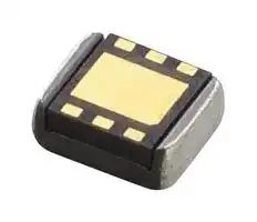
MYRLP250015F21RE
Non Isolated POL DC/DC Converter, ITE & Industrial, Step Down, Module, 1 Output, 2.5 V, 150 mA
⚠️ Reference pricing provided. In case of supply shortages, we will connect you with our trusted procurement partners to ensure your project's continuity.
- Manufacturer: MURATA POWER SOLUTIONS
- Product type: DC / DC Non Isolated Board Mount Converters - Fixed Output
- SVHC: No SVHC (04-Feb-2026)
- Depth: 2.5mm
- Width: 2mm
- Height: 1.04mm
- No. of Pins: 6Pins
- Product Range: PicoBK MYRLP-F-RE Series
- No. of Outputs: 1 Output
- Output Current: 150mA
- Output Power Max: -
- Input Voltage Max: 6V
- Input Voltage Min: 1.8V
- Output Current Max: 150mA
- Output Voltage Nom: 2.5V
- Input Voltage DC Max: 6V
- Input Voltage DC Min: 1.8V
- DC / DC Converter Type: Step Down, Module
- Operating Temperature Max: 85°C
- Power Supply Applications: ITE & Industrial
- DC / DC Converter Mounting: Surface Mount Device
- DC / DC Converter Output Type: Fixed
| Delivery and price | |
|---|---|
| Units per pack | 3000 |
| Price | 0.905 € |
| Current stock | 10+ |
| Lead time | 30 days |
Datasheet

## **“PicoBK** ™ **” MYRLP-F-RD/RE series**

Ultra-Low Quiescent Current, Inductor Built-in Step-Down DC/DC Converter

☆Green Operation compatible

## GENERAL DESCRIPTION

The MYRLP-F-RD/RE series is a synchronous step-down mini DC/DC converter which integrates an inductor and a control IC in one tiny package.

It uses an ultra-low current consumption circuit and PFM control. The control IC and coil are integrated to achieve miniaturization, and a space-saving power supply can be configured simply by adding two external capacitors. In addition, the ultra-low current consumption circuit and PFM control method realize high efficiency with a light load.

A operating voltage range of 1.8V to 6.0V enables support for applications that require an internally fixed output voltage from 0.5V to 3.60V. It has a built-in UVLO (Under Voltage Lock Out) function, the internalP-channel MOS driver transistor and N-channel MOS driver transistor are turned OFF when input voltage is below the UVLO detection voltage. The MYRLP-F-RD integrates CL discharge function which enables the electric charge at the output capacitor CL to be discharged via the internal discharge switch located between the VOUT and GND. When the devices enter stand-by mode, output voltage quickly returns to the VSS level as a result of this function.

## ■APPLICATIONS

- Smart meter

- Low Power RF

- Sensor Module

- Wearable Devices

- Energy Harvest devices

- Back-up power supply circuit

- Smart card

- Devices with 1 Lithium cell

## ■FEATURES

Input Voltage Range Output Voltage Setting Output VoltageAccuracy

Output Current Supply Current Control Method

Function

Protection Functions Input / Output Capacitor Operation Ambient Temperature

- : 1.8V ~ 6.0V

- : 0.5V ~ 3.60V

- : ±20mV (VOUT ≦ 1.0V) ±2.0% (VOUT > 1.0V)

- : 150mA

- : 200nA @ VOUT=1.8V

- : PFM control

- : CL Discharge (MYRLP-F-RD) UVLO function

- : Short Protection

- : Ceramic Capacitor Compatible : -40 ~ 85 ℃

Environmentally Friendly

- :   EU RoHS compliant, Pb Free Halogen Free

## ■TYPICAL APPLICATIONCIRCUIT

## ■ TYPICAL PERFORMANCE CHARACTERISTICS

## MYRLP-F-RD

**==> picture [460 x 160] intentionally omitted <==**

**----- Start of picture text -----**<br>
VOUT =1.8V, C =10μF, C =20μF,IN L Ta=25 ℃<br>100<br>VIN VIN L1 L x 90<br>80<br>CIN GND GND 70<br>VCE VOUT 60<br>CE VOUT<br>L2 50<br>40<br>CL Vin=2.7V<br>30 Vin=3.6V<br>aT 20 -——— Vin=4.2V<br>r a<br>10<br>< MYRLP-F-RD/RE Series > 0<br>0.001 0.01 0.1 1 10 100<br>EFFI[%]<br>**----- End of picture text -----**<br>


Export Control Code : X0863, Document No : D90DH - 00119

IOUT[mA]

MYRLP-F-RD/RE series A01 Page 1 of 26

## **“PicoBK** ™ **” MYRLP-F-RD/RE series**

Ultra-Low Quiescent Current, Inductor Built-in Step-Down DC/DC Converter

## Series ■ BLOCK DIAGRAM

**==> picture [100 x 8] intentionally omitted <==**

**----- Start of picture text -----**<br>
MYRLP-F-RD/RE Series<br>**----- End of picture text -----**<br>


- Diodes inside the circuits are ESD protection diodes and parasitic diodes.

MYRLP-F-RE does not have CL Dischargefunction.

MYRLP-F-RD/RE series A01 Page 2 of 26

## **“PicoBK** ™ **” MYRLP-F-RD/RE series**

Ultra-Low Quiescent Current, Inductor Built-in Step-Down DC/DC Converter

## ■ PIN CONFIGURATION

**==> picture [124 x 113] intentionally omitted <==**

**----- Start of picture text -----**<br>
L1<br>7<br>VIN 6 1 Lx<br>NC 5 2 GND<br>CE 4 3 VOUT<br>8<br>L2<br>**----- End of picture text -----**<br>


< BOTTOM VIEW >

* The dissipation pad should be solder-plated in recommended mount pattern and metal masking to enhance mounting strength and heat release.  If the pad needs to be connected to other pins, it should be connected to the GND (No.2) pin.

## ■ PINASSIGNMENT

|PIN NUMBER|PIN NAME|FUNCTION|
|---|---|---|
|1|Lx|Switching|
|2|GND|Ground|
|3|VOUT|Output Voltage|
|4|CE|Chip Enable|
|5|GND|Ground|
|6|VIN|Input Voltage|
|7|L1|Inductor Electrodes|
|8|L2|Inductor Electrodes|


- The NC (No.5) pin is not connected to the chip.

## ■FUNCTION

|PIN NAME|SIGNAL|STATUS|
|---|---|---|
|CE|H|Active|
||L|Stand-by|


* Please do not leave the CE pin open.

## ■PRODUCTION SUFFIX

MYRLP-F-RD/RE series A01 Page 3 of 26

Ultra-Low Quiescent Current, Inductor Built-in Step-Down DC/DC Converter

## **“PicoBK** ™ **” MYRLP-F-RD/RE series**

## ■ ABSOLUTE MAXIMUM RATINGS

|PARAMETER|SYMBOL|RATINGS|UNITS|
|---|---|---|---|
|VINPin Voltage|VIN|-0.3 ~ 7.0|V|
|Lx Pin Voltage|VLX|-0.3 ~ VIN+ 0.3 or 7.0 (*1)|V|
|VOUTPin Voltage|VOUT|-0.3 ~ VIN+ 0.3 or 7.0 (*1)|V|
|CE Pin Voltage|VCE|-0.3 ~ 7.0|V|
|Power Dissipation<br>(Ta=25℃)|Pd|TBD (JESD51-7board) (*2)|mW|
|Operating AmbientTemperature|Topr|-40 ~ 85|℃|
|Storage Temperature|Tstg|-55 ~ 125|℃|


- All voltages are described based on the GND pin.

(*1) The maximum value should be either VIN+0.3V or 7.0V in the lowest.

> (*2) The power dissipation figure shown is PCB mounted and is for reference only. The mounting condition is please refer to PACKAGING INFORMATION.

MYRLP-F-RD/RE series A01 Page 4 of 25

## **“PicoBK** ™ **” MYRLP-F-RD/RE series**

Ultra-Low Quiescent Current, Inductor Built-in Step-Down DC/DC Converter

## ■ ELECTRICAL CHARACTERISTICS

|PARAMETER|SYMBOL|CONDITIONS|CONDITIONS|MIN.|TYP.|MAX.|UNITS|CIRCUIT|
|---|---|---|---|---|---|---|---|---|
|Output Voltage(*1)|VOUT|When connected to external components,<br>IOUT= 30mA||-|<T-1>|-|V|①|
|Output Voltage1-2|VOUT1-2|Voltage which LXpin changes “H” to “L” level while VOUTis<br>increase. (*5)||<E-1>|<E-2>|<E-3>|V|②|
|Operating Voltage Range|VIN|-||<C-1>|-|6.0|V|①|
|Maximum Output Current|IOUTMAX|When connected to external components (*2)||150|-|-|mA|①|
|UVLO Release Voltage|VUVLOR|VOUT= 0.0V , VCE=1.8V<br>Voltage which Lxpin holding"H" level(*5)|Ta=25℃|-|1.50|1.78|V|②|
||||Ta=-40~85℃(*3)||||||
|UVLO Detect Voltage|VUVLOD|VOUT= 0.0V , VCE=1.8V<br>Voltagewhich Lxpin holding"L" level(*5)|Ta=25℃|1.00|1.40|-|V|②|
||||Ta=-40~85℃(*3)||||||
|Quiescent Current|Iq|VIN= VCE=<C-1>, VOUT=VOUT×1.05||-|<E-4>|<E-5>|nA|③|
|Stand-by Current|ISTB|VIN= VOUT=6.0V||-|0.0|0.1|μA|③|
|PFM Switching Current|IPFM|When connected to external components,<br>VIN= VOUT(T) + 2.0V,IOUT= 10mA||-|400|600|mA|①|
|Efficiency|EFFI|IOUT= 30mA||-|<E-6>|-|%|①|
|Lx SW ”H” ON Resistance|RLXH|VOUT= 0.0V,VIN= VCE= 5.0V, ILx = 50mA||-|0.35|0.45|Ω|④|
|Lx SW ”L” ON Resistance(*3)|RLXL|VIN= 5.0V||-|0.32|0.42|Ω|-|
|Lx SW ”H” Leakage Current|ILeakH|VIN= 6.0V , VOUT= VCE= 0.0V , VLx = 6.0V||-|0.0|0.1|μA|④|
|Lx SW ”L” Leakage Current|ILeakL|VIN= 6.0V , VOUT= VCE= 0.0V , VLx = 0.0V||-|0.0|0.1|μA|④|
|Output Voltage<br>Temperature<br>Characteristics|⊿VOUT/<br>(⊿VOUT・⊿Topr)|-40℃≦Topr ≦85℃<br>)<br>IOUT= 30mA||-|±100|-|ppm/℃|①|
|CE "H" Voltage|VCEH|VOUT= 0.0V,<br>Voltage which Lx pin holding “H” level(*5)|Ta=25℃|1.2|-|6.0|V|②|
||||Ta=-40~85℃(*3)||||||
|CE "L" Voltage|VCEL|VOUT= 0.0V,<br>Voltage which Lx pin holding “L” level(*5)|Ta=25℃|GND|-|0.3|V|②|
||||Ta=-40~85℃(*3)||||||
|CE “H” Current|ICEH|VIN= 6.0V, VOUT= 0.0V , VCE= 6.0V||-0.1|0.0|0.1|μA|⑤|
|CE “L” Current|ICEL|VIN= 6.0V, VOUT= 0.0V , VCE= 0.0V||-0.1|0.0|0.1|μA|⑤|
|Short Protection<br>Threshold Voltage(*4)|VSHORT|Voltage which Lx pin holding “L” level(*5)|Ta=25℃|0.10|0.54|0.80|V|②|
||||Ta=-40~85℃(*3)||||||
|CLDischarge (MYRLP-F-RD)|RDCHG|VIN= 5.0V, VCE= 0.0V, VOUT=0.1V||29|45|60|Ω|②|
|Inductance Value|L|Test Frequency=1MHz||-|2.2|-|μH||
|Inductor Rated Current|IDC_L|ΔT=+40℃<br>Current value that raises the temperature by 40℃<br>With DC current||-|850|-|mA||


## MYRLP-F-RD/RE Series

Unless otherwise stated, VIN=5V, VCE=5V, VOUT(T)=Nominal Value

(*1) VOUT are the average values of the output voltage considering the ripple voltage and they are set so that they can be a setting output voltage with this evaluation condition.

(*2) The maximum output current performance varies based on a voltage difference between an input voltage and an output voltage, and external components and so on. Regarding detail of this variation, please refer to OPERATIONAL EXPLANATION and NOTE ON USE section.

(*3) Design value

(*4) SHORT PROTECTION with LATCH is not available if VOUT1 is 1.2V or less.

(*5) "H" = VIN ~ VIN -1.2V, "L" = 0.1V ~ -0.1V

MYRLP-F-RD/RE series A01 Page 5 of 26

## **“PicoBK** ™ **” MYRLP-F-RD/RE series**

Ultra-Low Quiescent Current, Inductor Built-in Step-Down DC/DC Converter

## ■ ELECTRICAL CHARACTERISTICS

SPEC Table

|Part Number|NOMINAL<br>OUTPUT<br>VOLTAGE<br>VOUT(T)|VOUT(V)|VOUT1-2(V)|VOUT1-2(V)|VOUT1-2(V)|VIN(V)|Iq(nA)|Iq(nA)|
|---|---|---|---|---|---|---|---|---|
|||<T-1>|<E-1>|<E-2>|<E-3>|<C-1>|<E-4>|<E-5>|
|||TYP.|MIN.|TYP.|MAX.|VIN|TYP.|MAX.|
|MYRLP060015F21RD|0.60|0.600|0.560|0.580|0.600|1.80|200|600|
|MYRLP080015F21RD|0.80|0.800|0.760|0.780|0.800|1.80|200|600|
|MYRLP090015F21RD|0.90|0.900|0.860|0.880|0.900|1.80|200|600|
|MYRLP100015F21RD|1.00|1.000|0.960|0.980|1.000|1.80|200|600|
|MYRLP120015F21RD|1.20|1.200|1.156|1.180|1.204|1.80|200|600|
|MYRLP180015F21RD|1.80|1.800|1.744|1.780|1.816|2.30|200|600|
|MYRLP200015F21RD|2.00|2.000|1.940|1.980|2.020|2.50|210|630|
|MYRLP250015F21RD|2.50|2.500|2.430|2.480|2.530|3.00|220|660|
|MYRLP300015F21RD|3.00|3.000|2.920|2.980|3.040|3.50|230|690|
|MYRLP330015F21RD|3.30|3.300|3.214|3.280|3.346|3.80|240|720|
|MYRLP060015F21RE|0.60|0.600|0.560|0.580|0.600|1.80|200|600|
|MYRLP080015F21RE|0.80|0.800|0.760|0.780|0.800|1.80|200|600|
|MYRLP090015F21RE|0.90|0.900|0.860|0.880|0.900|1.80|200|600|
|MYRLP100015F21RE|1.00|1.000|0.960|0.980|1.000|1.80|200|600|
|MYRLP120015F21RE|1.20|1.200|1.156|1.180|1.204|1.80|200|600|
|MYRLP180015F21RE|1.80|1.800|1.744|1.780|1.816|2.30|200|600|
|MYRLP200015F21RE|2.00|2.000|1.940|1.980|2.020|2.50|210|630|
|MYRLP250015F21RE|2.50|2.500|2.430|2.480|2.530|3.00|220|660|
|MYRLP300015F21RE|3.00|3.000|2.920|2.980|3.040|3.50|230|690|
|MYRLP330015F21RE|3.30|3.300|3.214|3.280|3.346|3.80|240|720|


With regard to other voltage, please contact our sales representative.

MYRLP-F-RD/RE series A01 Page 6 of 25

## **“PicoBK** ™ **” MYRLP-F-RD/RE series**

Ultra-Low Quiescent Current, Inductor Built-in Step-Down DC/DC Converter

## ■ TEST CIRCUITS

**==> picture [202 x 176] intentionally omitted <==**

**----- Start of picture text -----**<br>
< Test Circuit No.① ><br>Wave Form Measure Point<br>aw L<br>~<br>oO<br>L1<br>1 Lx NC O<br>I OUT<br>i m VIN VOUT O —><br>V A CE GND CL<br>V<br>CIN L2<br>O O x“. 4 0 H 4b:<br>※ External Components<br>L : 2.2 μ H(For test process)<br>CIN : 10 μ F<br>CL     :10 μ F<br>**----- End of picture text -----**<br>


**==> picture [249 x 170] intentionally omitted <==**

**----- Start of picture text -----**<br>
< Test Circuit No.② ><br>Wave Form Measure Point<br>\<br>\\ O<br>\ L1<br>OO Ny Lx NC 0<br>T VIN VOUT O<br>Rpulldown<br>V A CE GND A V<br>CIN V L2<br>O O A OF1 0 r O A O<br>※ External Components<br>CIN : 10 μ F<br>Rpulldown : 100 Ω<br>**----- End of picture text -----**<br>


< Test Circuit No.③ >

< Test Circuit No.④ >

**==> picture [438 x 126] intentionally omitted <==**

**----- Start of picture text -----**<br>
L1 L1<br>C] Lx NC CO) Lx NC<br>VIN VOUT VIN VOUT<br>OQ A © V t O A<br>e V n e A o CE GND 0 A CE GND<br>IS is CIN L2 C4 CIN A L2<br>※   Ext ernal Components ※ External Components<br>CIN :10 μ F CIN : 0.1 μ F<br>**----- End of picture text -----**<br>


MYRLP-F-RD/RE series A01 Page 7 of 26

**“PicoBK** ™ **” MYRLP-F-RD/RE series**

Ultra-Low Quiescent Current, Inductor Built-in Step-Down DC/DC Converter

## ■ TYPICAL APPLICATIONCIRCUIT

**==> picture [194 x 84] intentionally omitted <==**

**----- Start of picture text -----**<br>
VIN L1<br>V IN L x<br>CIN NC GND<br>VCE VOUT<br>CE VOUT<br>L2<br>CL<br>**----- End of picture text -----**<br>


(NOTES): The coil is exclusively for this product.

Please do not use it for any purpose other than this product.

## 【 Typical Examples 】

||Manufacture|Product Number|Value|Size|
|---|---|---|---|---|
|CIN|Murata|GRM188R61A106ME69|10μF/10V|1.6 x 0.8 x 1.0mm|
|CL|Murata|GRM188R61A106ME69|10μF/10V|1.6 x 0.8 x 1.0mm|
|||GRM188R61A226ME15|22μF/10V||


Please select the components taking into consideration the rated voltage, rated current, and ceramic capacitor DC bias characteristics, etc. Use a ceramic capacitor with an execution capacitance value equal to or higher than the recommended component. If a capacitor with a low effective capacitance value is used, the output voltage may become unstable. Please increase a capacitance value for CL in order to reduce output ripple voltages.

CL such as tantalum capacitors which have a larger ESR value can increase output ripple voltages.

If large-capacity capacitors such as electrolytic capacitors are connected in parallel, the inrush current may increase at startup and the output voltage may become unstable.

MYRLP-F-RD/RE series A01 Page 8 of 25

## **“PicoBK** ™ **” MYRLP-F-RD/RE series**

Ultra-Low Quiescent Current, Inductor Built-in Step-Down DC/DC Converter

## ■ OPERATIONAL EXPLANATION

The MYRLP-F-RD/RE series consists of a reference voltage supply, PFM comparator, Pch driver FET, Nch driver FET,

current sensing circuit, PFM control circuit, CE control circuit, and others.

< BLOCK DIAGRAM >

The efficiency performance at a light load current is significantly improved compared to existing Murata products by implementing  a current limit PFM as a control method and reducing a consumption current by IC itself.

MYRLP-F-RD/RE series A01 Page 9 of 26

**“PicoBK** ™ **” MYRLP-F-RD/RE series**

Ultra-Low Quiescent Current, Inductor Built-in Step-Down DC/DC Converter

## ■OPERATIONAL EXPLANATION (Continued)

## .<Normal operation>

~ This IC controls the output voltage by adjusting the following ① ③ operation intervals in response to the output current. The VOUT output voltage average values during actual operation depend on VOUT and the ripple voltage during actual operation and are calculated as follows. For this reason, if the ripple voltage changes due to the influence of the input voltage, output voltage, or peripheral components, etc., the output voltage average value will change.

VOUT = VOUT1-2  + Ripple Voltage x 1/2

- ①The feedback voltage (FB voltage) is the voltage that results from dividing the output voltage with the VOUT Controller logic circuit. The PFM comparator compares this FB voltage to VREF. When the FB voltage is lower than VREF, the PFM comparator sends a signal to the PFM control circuit to turn on the Pch driver FET.

The On Time to Pch driver FET can be obtained by the following equation.

## tON  = L × IPFM  / (VIN - VOUT)

- ②When the Pch driver FET turns on, the coil current increases until the coil current reaches PFM Switching Current (IPFM). When the coil current reaches IPFM, the Pch driver FET turns off and then the Nch driver FET turns on.

- ③ After the Nch driver FET turns on, the coil current will decrease and when the coil current goes down to approx. 0mA, the Nch  driver FET will turn off.

The Pch driver FET and Nch driver FET remain off until the FB voltage becomes lower than the reference voltage VREF.

The above ①~③ switching operations increase the FB voltage accompanying the output voltage increase, but if the PFM comparator determines the FB voltage is lower than the reference voltage VREF before the coil current reaches 0mA, the Nch driver FET turns off and the status moves to ①.

**==> picture [468 x 250] intentionally omitted <==**

**----- Start of picture text -----**<br>
V OUT   rs rs es a TTT Ripple<br>V OUT1-2 _ a4dosbe<i— 1 a a  4S 1 i annaee ! —i1_ et Ripple Voltage x1/2 -- SfTT Voltage<br>i} l i} l l<br>i} I i} I I<br>i} I i} I I<br>i} l i} l l<br>1I1II<br>Ii} I i} i}<br>I i} I i} i}<br>0V<br>—-a--1---3----~-& 1 l 1 --- 3-1 l l<br>i} I i} I I<br>i}1 tON II i}i} II tON II<br>it > i} it ><br>1<br>I<br>I<br>1<br>Lx 1<br>[J l<br>i} l<br>——_— i} — ee I — ——— 0V<br>1I1II<br>I i} I i} i}<br>I i} I i} i}<br>IPFM re So i eesse se SS TT<br>1 1 l<br>Coil   i}i} i}i} ll<br>Current i} i} I<br>11l<br>11 I<br>IOUT III<br>aSS 0mA<br>**----- End of picture text -----**<br>


MYRLP-F-RD/RE series A01 Page 10 of 25

**“PicoBK** ™ **” MYRLP-F-RD/RE series**

Ultra-Low Quiescent Current, Inductor Built-in Step-Down DC/DC Converter

## ■ OPERATIONAL EXPLANATION (Continued)

< Maximum on-time function, 100% Duty operation>

When the input / output potential difference decreases, the on-time required for the coil current to reach IPFM increases,

and the  output ripple voltage tends to increase.Therefore, under conditions where the input / output potential difference is small, excessive  ripple voltage is suppressed by limiting the maximum on-time that the Pch driver FET can turn on after the FB voltage becomes  higher than the reference voltage VREF to 3.0μs(TYP.).

If the input / output potential difference is further reduced, the FB voltage is always lower than the reference voltage VREF, so the 100% duty operation is performed and the Pch driver FET is always on.

At 100% duty, the current consumption of the IC increases compared to normal operation.

**==> picture [467 x 246] intentionally omitted <==**

**----- Start of picture text -----**<br>
VOUT 47-4 i SoRr-r4tIe 1 i srr I 1 Ripple<br>VOUT1-2 a i]i I I i]fl Ii ee er oe eeI I  eS ] Ripple Voltage x1/2 =~ Voltage<br>III<br>I I I I I<br>IIII<br>II I I I<br>i] I i] I I<br>I I I I I<br>0V<br>——a—-—-—--ba-——-—--& i] I i] -- I I<br>IIII<br>i] I tON_MAX II II II tON_MAX II<br>< —m  —_ I << —,<br>IIII<br>I I I I I<br>i] I i] I I<br>iIi<br>Lx I<br>II<br>I fl<br>I I<br>—— oy Se ——— 0V<br>i] I i] I I<br>fl I fl I I<br>I I I I I<br>IPFM ia<br>I I I I I<br>IIII<br>Coil   I I I<br>Curren t III<br>II I<br>III<br>IOUT I ASASS I I a 0m A<br>**----- End of picture text -----**<br>


MYRLP-F-RD/RE series A01 Page 11 of 26

**“PicoBK** ™ **” MYRLP-F-RD/RE series**

Ultra-Low Quiescent Current, Inductor Built-in Step-Down DC/DC Converter

## ■OPERATIONAL EXPLANATION (Continued)

## <CE function>

When "H" voltage (VCEH) is fed to the CE pin, normal operation starts after raising the output voltage with Start-up Mode. When the "L" voltage (VCEL) is fed to the CE pin, it enters the stand-by state and the current consumption is suppressed to 0.0μA (TYP.). Additionally, Pch MOS driver FET and Nch MOS driver FET are turned off.

## <Start-up Mode>

After “H” voltage (VCEH) is fed to CE pin and UVLO function is released, by the time when FB voltage goes up to 0.9 x VREF, the startup mode operates.

Unlike the normal operation, the start-up mode stops the operation of the short-circuit protection function and prevents the IC from being inadvertently stopped.

In order to suppress the inrush current, the peak current of the coil is limited to 0.7 x IPFM, and the Nch driver FET does not turn on and the coil current flows through the parasitic diode of the Nch driver FET.

The rise time of the output voltage depends on the output capacitance and output current.

**==> picture [538 x 325] intentionally omitted <==**

**----- Start of picture text -----**<br>
Start-up Mode<br>(Start-up time Depend on CL,Iout) Normal operation Stand-by<br>Ss<br>| | l<br>0.9 x VOUT(T) |-t—---------se- - -----<br>| -- - - --- - f--<br>VOUT MYRLP-F-RE<br>|1 | | |ll MYRLP-F-RD ANSI.oN (Fall time depends onIout)<br>ee<br>0V<br>TI |<br>|||<br>FB 0.9 x VREF a I-T |ee|l \ MYRLP-F-RE<br>Voltage |<br>| | MYRLP-F-RD A<br>Poteet 0V<br>TI<br>||l<br>| | l l<br>Coil   IPFM Lo my my aps yoo<br>Current 0.7 x IPFM a<br>|| l<br>| | l |<br>—~V_-V¥_V_VoV_ 8 __ — 0mA<br>||l<br>| | | |<br>1<br>VCE / /I| |l |l<br>VCEH<br>VCEL Sy 0V<br>**----- End of picture text -----**<br>


## <UVLO function>

When the VIN voltage becomes UVLO Detect Voltage (VUVLOD) or less, the UVLO function operates to forcibly turn off the Pch MOS driver FET to prevent erroneous pulse output due to operation instability of the internal circuit.

During the UVLO function, the Pch driver FET and Nch driver FET turn off, and the Nch FET M1 between the VOUT pin and GND pin turns on to discharge the output capacitance and make the output voltage be lower.

When the VIN voltage becomes UVLO Release Voltage (VUVLOR) or more, the UVLO function is canceled.After the UVLO function is canceled, the output voltage rises with the startup mode, and then the normal operation is performed.

Moreover, during the UVLO operation, the current consumption increases because the internal circuit is operating and the switching operation is stopped, not the stand-by state.

MYRLP-F-RD/RE series A01 Page 12 of 25

## **“PicoBK** ™ **” MYRLP-F-RD/RE series**

Ultra-Low Quiescent Current, Inductor Built-in Step-Down DC/DC Converter

## ■ OPERATIONAL EXPLANATION (Continued)

## ・Case (a) : VOUT ≧1.2V

The short-circuit protection function monitors the VOUT pin voltage, and if the VOUT pin voltage drops below the Short Protection Threshold Voltage (VSHORT) due to a short circuit or overcurrent, the short circuit protection function operates.

When the short-circuit protection function is activated, the Pch driver FET and Nch driver FET are held off. If the VOUT pin voltage exceeds the Short Protection Threshold Voltage (VSHORT) after the short-circuit protection function is activated, normal operation resumes.

To cancel the short-circuit protection function, it is necessary to start the IC after putting the IC in the standby state with the CE function, or to raise the input voltage after setting the input voltage below the UVLO detection voltage (VUVLOD).

**==> picture [499 x 288] intentionally omitted <==**

**----- Start of picture text -----**<br>
Short or Overcurrent   Start-up &   Short or Overcurrent Start-up &<br>Normal operation i} Condition 1 Normal operation I Condition I Normal operation<br>Oo<br>i} OO [| I I I| —_———————><br>VOUT Jde----- i} ee ee ee ee ed rt de ee eee beo------- I e eL I eL I  e e eee - VOUT(T)<br>1 tt I I I<br>VSHORT ---- eee lee eee ee ee LLtt NL f I — eeeee HH Kee<br>ss se es cs ecee 0V<br>i} [| I I I<br>i} It I I I<br>i} rt I I I<br>IPFM ey ee ee pe ee eh ee eh ee ee eee<br>0.7 xI PFM -A--A- a nn<br>Coil   !! Ittl !! !! OO I] nee A Oy AV<br>Current ~ 11 111 IT U Td l 0mA<br>— — i} It I I I<br>! It ! ! l<br>i} I<br>RLoad !! rtIl !I !! II<br>! tl I ! ] Ω<br>—--- - -eas 0<br>i} [| ee eo OO Seana I tateI I ee ee:<br>i} [| I I I<br>i} I I I<br>VCE VCEH   wee ee ee i} bee ee ee ee ee eee ee wee ee eee ee eh I ee ee ee ee ee I qe I ee ee ee ee ee ee<br>VCEL es eee ee eee eee ee eh ee ee ee ee ee ee ee ee ee ee ee eee 0V<br>i} I I I<br>a, a a a a i as<br>i} [| Restart I I I<br>i} rt I I I<br>T ! I<br>! 1 ! I<br>VUVLOH   -------Le---~ eee ee ee ee ee ee eb Le ee ee ee ee ee ee ee ee ee fee ee ee ee ee<br>VIN VUVLOD eee ee ee i} bee ee ee ee ee ee ee ee eb [| Ee ee Ke ee ee ee ek I ee ee ee ee ef ee fe I ee ee ee eee ee eee<br>i} it I I 0V<br>a, a i a a pHoO--------<br>Restart<br>**----- End of picture text -----**<br>


・Case (b) : VOUT <1.2V

The short-circuit protection function is not implemented in the part numbers where VOUT is less than 1.2V. If a short circuit or overcurrent occurs, the output voltage will drop and switching operation will continue.

When the short-circuit state or excessive output current is released, the output voltage rises quickly to the set output voltage.

**==> picture [499 x 165] intentionally omitted <==**

**----- Start of picture text -----**<br>
Normal operation Short or Overcurrent Condition Normal operation<br>i i} ps * E<br>VOUT deo------ 1 eee ee ee ee ee ee ee ee ee ee T eee VOUT(T)<br>VSHOR T mr fl rr rr rr rt i}i} foo rr rrr rrr<br>—- SS ES ES ES ES EO OOOOOOONDSaaaeaaneanannennnneneauaawwwaoaoananna"—ES ES ES ES EE Ee Ee nnn 0V<br>I i}<br>I i}<br>I 1<br>IPFM _—_2 epee . . . — . . . . a . . J! . — —s . . — —s . . — —s<br>I i}<br>Coil   i}I i}<br>Current — —  EEannsilanitaneianetiantianstianetantiansttonntionstiemstentiantientientoni} ba = —_ — — _— - 0mA<br>— Se 1 !<br>I i}<br>i}<br>RLoad 1i}<br>SESE 1 OOOO Oe eee a 0Ω<br>**----- End of picture text -----**<br>


MYRLP-F-RD/RE series A01 Page 13 of 26

## **“PicoBK** ™ **” MYRLP-F-RD/RE series**

Ultra-Low Quiescent Current, Inductor Built-in Step-Down DC/DC Converter

## ■OPERATIONAL EXPLANATION (Continued)

< CL Discharge function (MYRLP-F-RD)>

On the MYRLP-F-RD/RE series, a CL discharge function is available as an option.

CL discharge function turns on the Nch FET M1 between the VOUT pin and GND pin when the stand-by condition in order to discharge the output capacitance quickly and make the output voltage be lower.

This prevents malfunctioning of the application in the event that a charge remains on CL when the IC is stand-by state.

The discharge time is determined by CL and the CL discharge resistance RDCHG, including the Nch FET M1. the discharge time of the output voltage is calculated by means of the equation below.

V = VOUT(T) × e[- t/ τ] t =   In(V τ OUT(T)  /V)

V : Output voltage during discharge VOUT(T) : Outputvoltage t : Discharge time CL : Effective capacitance of Output capacitor RDCHG : CL auto-discharge resistance τ : CL × RDCHG

MYRLP-F-RD/RE series A01 Page 14 of 25

## **“PicoBK** ™ **” MYRLP-F-RD/RE series**

Ultra-Low Quiescent Current, Inductor Built-in Step-Down DC/DC Converter

## ■ NOTE ON USE

1. Be careful not to exceed the absolute maximum ratings for externally connected components and this IC.

2. The DC/DC converter characteristics greatly depend not only on the characteristics of this IC but also on those of externally connected components, so refer to EXTERNAL COMPONENTS SELECTION and the specifications of each component and be careful when selecting the components. Be especially careful of the characteristics of the capacitor used for the load capacity CL and use a capacitor with B characteristics (JIS Standard) or an X7R/X5R (EIA Standard) ceramic capacitor.

3. The CE pin and VSET pin does not have an internal pull-up or pull-down, etc. Apply the prescribed voltage to the CE pin and VSET pin.

- If an intermediate voltage is fed to the CE and VSET pins, a through current will flow through the input stage of the CE and VSET pins, increasing current consumption.

4. At light loads or when IC operation is stopped, leakage current from the Pch driver FET may cause the output voltage to rise.

5. Switching operation may be performed continuously due to internal delay or input offset of the PFM comparator circuit. If the switching operation continues, the output ripple voltage increases and the output voltage rises as the ripple voltage increases.

6. When the input / output potential difference is small, the ripple voltage increases and the output voltage may increase.

7. Since the short-circuit protection function is not implemented in the part number where both of or either VOUT is less than 1.2V, the coil current may be superposed under the condition of high input voltage and excessive output current.

8. During start-up mode, the peak current of the coil is set lower than in normal operation, so the output voltage may not rise under conditions where the output current is large during start-up.

9. To suppress current consumption, UVLO detection is performed only for a certain period after the Pch driver FET is turned on. For this reason, the UVLO function may not operate if the VIN pin voltage instantaneously drops below the UVLO detection voltage (VUVLOD).

10. For temporary, transitional voltage drop or voltage rising phenomenon, the IC is liable to malfunction should the ratings be exceeded.

11. Murata places an importance on improving our products and their reliability. We request that users incorporate fail-safe designs  and post-aging protection treatment when using Murata products in their systems.

MYRLP-F-RD/RE series A01 Page 15 of 26

**“PicoBK** ™ **” MYRLP-F-RD/RE series**

Ultra-Low Quiescent Current, Inductor Built-in Step-Down DC/DC Converter

## ■NOTE ON USE (Continued)

## 12. Instructions of pattern layouts

(1)In order to stabilize VIN voltage level, we recommend that a by-pass capacitor (CIN) be connected as close as possible to the VIN & GND pins.

- (2) Please mount each external component as close to the IC as possible.

- (3) Wire external components as close to the IC as possible and use thick, short connecting traces to reduce the circuit impedance.

- (4) Make sure that the PCB GND traces are as thick as possible, as variations in ground potential caused by high ground currents at the time of switching may result in instability of the IC.

- (5) This series’ internal driver FET bring on heat because of the output current and ON resistance of Pch driver FET.

< Reference pattern layout >

**==> picture [203 x 9] intentionally omitted <==**

**----- Start of picture text -----**<br>
Layer 1 Layer 2<br>**----- End of picture text -----**<br>


**==> picture [200 x 8] intentionally omitted <==**

**----- Start of picture text -----**<br>
Layer 3 Layer 4<br>**----- End of picture text -----**<br>


MYRLP-F-RD/RE series A01 Page 16 of 25

## **“PicoBK** ™ **” MYRLP-F-RD/RE series**

Ultra-Low Quiescent Current, Inductor Built-in Step-Down DC/DC Converter

## ■ Notes on handling of product

(1) The coil mounted on this product complies with the general surface mount type chip inductor specifications, and may have scratches, flux stains, etc.

(2) Do not use this product in the following environments. Places exposed to water or salt water, places where condensation occurs, places where toxic gases (hydrogen sulfide, zinc acid, chlorine, ammonia, etc.) are present.

(3) Please do not wash this product with solvent.

## ■ Notes on mounting

(1) Please set the mounting position accuracy within 0.05 mm.

MYRLP-F-RD/RE series A01 Page 17 of 26

Ultra-Low Quiescent Current, Inductor Built-in Step-Down DC/DC Converter

## **“PicoBK** ™ **” MYRLP-F-RD/RE series**

## ■ TYPICAL PERFORMANCE CHARACTERISTICS

(1) Efficiency vs. Output Current

MYRLP-F-RD/RE (VOUT=1.8V)

MYRLP-F-RD/RE (VOUT=3.0V)

**==> picture [196 x 604] intentionally omitted <==**

**----- Start of picture text -----**<br>
1009080 eseelee<br>70 4A ee<br>60 CA | VIN =4.2V<br>5040 eaoTFd VIN =3.6VVIN =2.7V II<br>3020100 eseses eeeeee ee<br>0.001 0.01 0.1 1 10 100<br>Output Current: IOUT (mA)<br>MYRLP-F-RD/RE (VOUT=1.8V)<br>100<br>0, LE<br>~wiA tL. dL<br>oe<br>eg a<br>jw)<br>0.001 0.01 0.1 1 10 100<br>Output Current: IOUT (mA)<br>MYRLP-F-RD/RE (VOUT=1.8V)<br>100<br>ee aad<br>es, ce<br>on<br>en Ca<br>Bl el ee el<br>0.001 0.01 0.1 1 10 100<br>Output Current: IOUT (mA)<br>Efficiency: EFFI (%)<br>Efficiency: EFFI (%)<br>Efficiency: EFFI (%)<br>**----- End of picture text -----**<br>


**==> picture [193 x 605] intentionally omitted <==**

**----- Start of picture text -----**<br>
100<br>90 es<br>80 eee ee<br>70<br>AG<br>60 in rn rr VIN = 5.0V<br>50<br>VIN = 4.2V<br>403020100 fFeeTIeseses eeer<br>0.001 0.01 0.1 1 10 100<br>Output Current: IOUT (mA)<br>MYRLP-F-RD/RE (VOUT=3.0V)<br>100<br>i eee e a<br>i alre<br>ne<br>es<br>oe el ed<br>0.001 0.01 0.1 1 10 100<br>Output Current: IOUT (mA)<br>MYRLP-F-RD/RE (VOUT=3.0V)<br>100<br>ol wee<br>eS se<br>on es<br>es<br>ol el<br>0.001 0.01 0.1 1 10<br>Output Current: IOUT (mA)<br>Efficiency: EFFI (%)<br>Efficiency: EFFI (%)<br>Efficiency: EFFI (%)<br>**----- End of picture text -----**<br>


MYRLP-F-RD/RE series A01 Page 18 of 25

Ultra-Low Quiescent Current, Inductor Built-in Step-Down DC/DC Converter

## **“PicoBK** ™ **” MYRLP-F-RD/RE series**

## ■TYPICAL PERFORMANCE CHARACTERISTICS (Continued)

## (2) Output Voltage vs. Output Current

MYRLP-F-RD/RE (VOUT=1.8V)

MYRLP-F-RD/RE (VOUT=3.0V)

**==> picture [426 x 388] intentionally omitted <==**

**----- Start of picture text -----**<br>
2.00 3.30<br>1.95 ee VIN = 4.2V 3.25 VIN = 5.0V<br>VIN = 3.6V 3.20<br>1.90 Pf | ee n | 3.15 ee<br>VIN = 2.7V VIN = 4.2V<br>3.10<br>1.85<br>3.05<br>1.80 pf) | || 3.00 a<br>1.75 PP oo 2.95 a<br>2.90<br>1.70 Ff 2.85 i<br>1.65 eeffee 2.80 esi<br>2.75<br>1.60 ee ee ee ee 2.70 nna<br>0.001 0.01 0.1 1 10 100 0.001 0.01 0.1 1 10 100<br>Output Current: IOUT (mA) Output Current: IOUT (mA)<br>(3) Ripple Voltage vs. Output Current<br>MYRLP-F-RD/RE (VOUT=1.8V)   MYRLP-F-RD/RE (VOUT=3.0V)<br>100 100<br>90 ee es VIN = 4.2V ee 90 a eee0 VIN = 5.0V<br>80 7 VIN = 3.6V 4 80 —A~—O VIN = 4.2V O G<br>7060 |ee ee VIN = 2.7V eePo 7060 aeeee<br>50 ee ee ee 50 eeee ee<br>40 ee ee ee 40 eees ee<br>3020 Poee eee a 3020 PoPeeeeOYea<br>100 Peee en 100 eePteeeee eeeee<br>0.1 1 10 100 0.1 1 10 100<br>Output Current: IOUT (mA) Output Current: IOUT (mA)<br> (V)  (V)<br>OUT OUT<br>Output Voltage: V Output Voltage: V<br>Ripple Voltage: Vr (mV) Ripple Voltage: Vr (mV)<br>**----- End of picture text -----**<br>


- (3) Ripple Voltage vs. Output Current

- (4) Output Voltage vs. Ambient Temperature

- (5) UVLO Voltage vs. AmbientTemperature

MYRLP-F-RD/RE (VOUT=1.8V)

MYRLP-F-RD/RE

**==> picture [440 x 146] intentionally omitted <==**

**----- Start of picture text -----**<br>
IOUT = 30mA<br>1.90 1.8<br>1.88 ee 1.7 o_o] UVLO Release Voltage<br>1.86 ee rt<br>1.6<br>1.84 UVLO Detect Voltage<br>1.5<br>1.82 -—— ||} ee eee<br>1.80 Se 1.4 PF<br>1.78 ee 1.3 ee ee eee<br>1.76<br>1.74 poa 1.2 eeee eee<br>ee ee ee 1.1 ee ee ee<br>1.72<br>1.70 -—_{—_}ee | _f {| 1.0 Ff fF<br>-50 -25 0 25 50 75 100 -50 -25 0 25 50 75 100<br>Ambient Temperature: Ta ( ℃ ) Ambient Temperature: Ta ( ℃ )<br>(V)<br>OUT<br>Output Voltage: V UVLO Voltage (V)<br>**----- End of picture text -----**<br>


MYRLP-F-RD/RE series A01 Page 19 of 26

**“PicoBK** ™ **” MYRLP-F-RD/RE series** Ultra-Low Quiescent Current, Inductor Built-in Step-Down DC/DC Converter

## ■TYPICAL PERFORMANCE CHARACTERISTICS (Continued)

- (6) Quiescent Current vs. Ambient Temperature

- (7) Stand-by Current vs. Ambient Temperature

MYRLP-F-RD/RE (VOUT=0.6V)

MYRLP-F-RD/RE

**==> picture [190 x 360] intentionally omitted <==**

**----- Start of picture text -----**<br>
500<br>450 pes VIN=4.2V ee eee<br>400 VIN=3.6V<br>350 | | ee<br>VIN=1.8V<br>300250 |_||eeEeefF<br>200<br>150 eee ee eeeee ee<br>a ee<br>100 eeee eeeee<br>50<br>0-50 -25 0 25 50 75 100<br>Ambient Temperature: Ta ( ℃)<br>(8) PFM Switching Current vs. Ambient Temperature<br>MYRLP-F-RD/RE (VOUT=0.6V)<br>600 IOUT = 30mA<br>500<br>VIN  [= 5.0V]<br>400<br>300<br>200<br>100<br>0<br>-50 -25 0 25 50 75 100<br>Ambient Temperature: Ta ( ℃)<br>Quiescent Current: Iq (nA)<br> (mA)<br>PFM<br>PFM Switching Current: I<br>**----- End of picture text -----**<br>


- (8) PFM Switching Current vs. Ambient Temperature

**==> picture [202 x 133] intentionally omitted <==**

**----- Start of picture text -----**<br>
1.0<br>0.8<br>0.6<br>0.4<br>0.2 VIN = 6.0V<br>0.0<br>-50 -25 0 25 50 75 100<br>Ambient Temperature: Ta ( ℃)<br>STB<br>Standby Current: I (μA)<br>**----- End of picture text -----**<br>


- (9) CE ”H” Voltage vs. Ambient Temperature

MYRLP-F-RD/RE

**==> picture [195 x 131] intentionally omitted <==**

**----- Start of picture text -----**<br>
1.2<br>VIN = 5.0V<br>1.0 P| | le VIN = 3.6V " 7<br>0.8 VIN = 1.8V<br>|_| | | i<br>0.6 |r<br>0.4<br>P| | |tt<br>0.2<br>P| ft tT<br>0.0 | | | |Ttft ff<br>-50 -25 0 25 50 75 100<br>Ambient Temperature: Ta ( ℃)<br> (V)<br>CEH<br>CE ”H” Voltage : V<br>**----- End of picture text -----**<br>


- (10) CE ”L” Voltage vs. Ambient Temperature

- (11) Short Protection Threshold vs. Ambient Temperature

MYRLP-F-RD/RE

MYRLP-F-RD/RE (VOUT=0.6V)

**==> picture [433 x 150] intentionally omitted <==**

**----- Start of picture text -----**<br>
1.2 1.4<br>VIN = 5.0V 1.2 VIN = 5.0V<br>1.0<br>ee e VIN = 3.6V e e || ft VIN =3.6V<br>1.0<br>0.8 re VIN = 1.8V VIN = 1.8V<br>0.8<br>0.6<br>SE 0.6 a<br>0.4 P| | 0.4 SS<br>0.2 po} | | ft 0.2 ee ee<br>0.0 TTT 0.0 ee<br>-50 -25 0 25 50 75 100 -50 -25 0 25 50 75 100<br>Ambient Temperature: Ta ( ℃) Ambient Temperature: Ta ( ℃)<br> (V)<br>SHORT<br> (V)<br>CEL<br>CE ”L” Voltage : V<br>Short Protection Threshold Voltage : V<br>**----- End of picture text -----**<br>


MYRLP-F-RD/RE series A01 Page 20 of 25

**“PicoBK** ™ **” MYRLP-F-RD/RE series**

Ultra-Low Quiescent Current, Inductor Built-in Step-Down DC/DC Converter

## ■ TYPICAL PERFORMANCE CHARACTERISTICS (Continued)

**==> picture [55 x 6] intentionally omitted <==**

**----- Start of picture text -----**<br>
MYRLP-F-RD/RE<br>**----- End of picture text -----**<br>


## MYRLP-F-RD

## MYRLP-F-RD

## MYRLP-F-RD

## MYRLP-F-RD

MYRLP-F-RD/RE series A01 Page 21 of 26

**“PicoBK** ™ **” MYRLP-F-RD/RE series** Ultra-Low Quiescent Current, Inductor Built-in Step-Down DC/DC Converter

## ■TYPICAL PERFORMANCE CHARACTERISTICS (Continued)

MYRLP-F-RD

## MYRLP-F-RD

MYRLP-F-RD/RE series A01 Page 22 of 25

## **“PicoBK** ™ **” MYRLP-F-RD/RE series**

Ultra-Low Quiescent Current, Inductor Built-in Step-Down DC/DC Converter

## ■PACKAGING INFORMATION

## ●Packaging (2.0mm×2.5mm, h=1.0mm)

**==> picture [246 x 46] intentionally omitted <==**

**----- Start of picture text -----**<br>
(unit: mm)<br>■外部リード処理Terminal material : Copper foil<br>Terminal plating : 1~6 Gold plating<br>7~8 Lead(Pb) free Solder plating<br>**----- End of picture text -----**<br>


**==> picture [425 x 205] intentionally omitted <==**

**----- Start of picture text -----**<br>
●Reference Pattern Layout (unit:mm) ●Reference Metal Mask Design (unit:mm)<br>2.9 2.85<br>0.4 1.3 0.4 0.5 1.2 0.5<br>0.35 0.3<br>- mi ze (4 = : 4<br>Biv 7 : FTL<br>0.4 0.4 0.4<br>[Z VW [7 [7 [7 ; n<br>0.55 0.55 0.55 0.55<br>Z Ls — - 0<br>y 0.4 ee 2.1 | 0.4 0.325 - 2.2 - 0.325<br>0.3<br>0.375<br>0.9 2.1 2.25 0.8 2.05 2.2<br>0.3<br>0.375<br>**----- End of picture text -----**<br>


*Please use the above mount pad dimensions and metal mask design as reference data.

MYRLP-F-RD/RE series A01 Page 23 of 26

## **“PicoBK** ™ **” MYRLP-F-RD/RE series**

Ultra-Low Quiescent Current, Inductor Built-in Step-Down DC/DC Converter

## ■PACKAGING INFORMATION

## Power Dissipation

Power dissipation data for the package is shown in this page. The value of power dissipation varies with the mount board conditions. Please use this data as one of reference data taken in the described condition.

## 1. Measurement Condition (Reference data) oo

Condition: Mount on a board

Ambient: Natural convection

Soldering: Lead (Pb) free

Board Dimensions: 40 x 40 mm (1600mm[2 ] in one side) Copper (Cu) traces occupy 50% of the board  area In top and back faces Package heat-sink  is tied to the copper traces

Material: Glass Epoxy (FR-4) Thickness: 1.6 mm Through-hole: 4 x 0.8 Diameter

Copper foil thickness: Front 35um, Back 35um

Evaluation Board (Unit:mm)

## 2. Power Dissipation vs. Ambient Temperature

Board Mount ( Tjmax=125℃)

|Ambient Temperature<br>(℃)|Power Dissipation Pd (mW)|Power Dissipation Pd (mW)|Thermal Resistance (℃/W)|
|---|---|---|---|
||Ta max=85℃|Ta max=105℃||
|25|800|800|125.00|
|85|320|320||
|105|0|160||
|125|0|0||


MYRLP-F-RD/RE series A01 Page 24 of 26

## **“PicoBK** ™ **” MYRLP-F-RD/RE series**

Ultra-Low Quiescent Current, Inductor Built-in Step-Down DC/DC Converter

## ■MARKING RULE

Mark①represents product series.

|MARK|PRODUCT SERIES|
|---|---|
|A|MYRLP***015F21RD / MYRLP***015F21RE|


**==> picture [447 x 224] intentionally omitted <==**

**----- Start of picture text -----**<br>
1 6<br>5! : —| Mark②,③ represents the registered setting, output voltage.<br>2 a4 a Lie 5<br>OUTPUT PRODUCT<br>3 I BGL 1Lie 4 MARK Type VOLTAGE(V) SERIES<br>E 0.50 ~ 3.60V MYRLP***015F21RE<br>15<br>D 0.50 ~ 3.60V MYRLP***015F21RD<br>i PA<br>Mark ④⑤ ,represents production lot number<br>01 ~ 09 、 0A ~ 0Z 、 11 ~ 9Z 、 A1 ~ A9 、 AA ~ ZZ 、 B1 ~ ZZ in order.<br>①<br>④ ②<br>⑤ ③<br>**----- End of picture text -----**<br>


(G, I, J, O, Q, W excluded) * No character inversion used.

MYRLP-F-RD/RE series A01 Page 25 of 25

**“PicoBK** ™ **” MYRLP-F-RD/RE series**

Ultra-Low Quiescent Current, Inductor Built-in Step-Down DC/DC Converter

1. The product and product specifications contained herein are subject to change without notice to improve performance characteristics. Consult us, or our representatives before use, to confirm that the information in this datasheet is up to date.

2. The information in this datasheet is intended to illustrate the operation and characteristics of our products. We neither make warranties or representations with respect to the accuracy or completeness of the information contained in this datasheet nor grant any license to any intellectual property rights of ours or any third party concerning with the information in this datasheet.

3. Applicable export control laws and regulations should be complied and the procedures required by such laws and regulations should also be followed, when the product or any information contained in this datasheet is exported.

4. The product is neither intended nor warranted for use in equipment of systems which require extremely high levels of quality and/or reliability and/or a malfunction or failure which may cause loss of human life, bodily injury, serious property damage including but not limited to devices or equipment used in 1) nuclear facilities, 2) aerospace industry, 3) medical facilities, 4) automobile industry and other transportation industry and 5) safety devices and safety equipment to control combustions and explosions. Do not use the product for the above use unless agreed by us in writing in advance.

5. Although we make continuous efforts to improve the quality and reliability of our products; nevertheless Semiconductors are likely to fail with a certain probability. So in order to prevent personal injury and/or property damage resulting from such failure, customers are required to incorporate adequate safety measures in their designs, such as system fail safes, redundancy and fire prevention features.

6. Our products are not designed to be Radiation-resistant.

7. Please use the product listed in this datasheet within the specified ranges.

8. We assume no responsibility for damage or loss due to abnormal use.

9. All rights reserved. No part of this datasheet may be copied or reproduced unless agreed by Murata Manufacturing Co., Ltd in writing in advance.

Murata Manufacturing Co., Ltd

MYRLP-F-RD/RE series A01 Page 26 of 26
Updated at April 29, 2026
About Novapart
Novapart is a B2B electronic component broker specialising in stock shortages and cost reduction. We source hard-to-find parts and identify compliant alternatives across a catalogue of 410,000+ components from 500+ manufacturers.
Learn more →Stock Shortage Specialist
When a component is unavailable, discontinued or has an unacceptable lead time, we tap into our network of vetted European and Asian distributors to source what you need — without compromising on quality or traceability.
Request a quote →Compliant Alternatives
We identify pin-to-pin, electrically equivalent substitutes that meet the same certifications (RoHS, AEC-Q100, REACH) as your original specification — validated against datasheets, not just part numbers. Often at a lower cost.
BOM Analysis service →