
Image not available
Illustrative purposes only

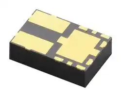
MYRGM080200X41RA
Non Isolated POL DC/DC Converter, ITE & Industrial, Step Down, Module, 900 mV, 6 V, 2 A
⚠️ Reference pricing provided. In case of supply shortages, we will connect you with our trusted procurement partners to ensure your project's continuity.
- Manufacturer: MURATA POWER SOLUTIONS
- Product type: DC / DC Non Isolated Board Mount Converters - Adjustable Output
- SVHC: No SVHC (04-Feb-2026)
- Depth: 3.1mm
- Width: 4.7mm
- Height: 1.35mm
- Topology: Synchronous Buck (Step Down)
- No. of Pins: 11Pins
- Product Range: PicoBK MYRGM-X Series
- No. of Outputs: 1 Output
- Output Current: 2A
- Output Power Max: -
- Input Voltage Max: 6V
- Input Voltage Min: 2.7V
- Output Current Max: 2A
- Output Voltage Max: 6V
- Output Voltage Min: 900mV
- Switching Frequency: 2.4MHz
- Input Voltage DC Max: 6V
- Input Voltage DC Min: 2.7V
- DC / DC Converter Type: Step Down, Module
- DC / DC Converter IC Case: SMD
- Operating Temperature Max: 85°C
- Power Supply Applications: ITE & Industrial
- DC / DC Converter Output Type: Adjustable
| Delivery and price | |
|---|---|
| Units per pack | 500 |
| Price | 0.792 € |
| Current stock | 10+ |
| Lead time | 30 days |
Datasheet

**“PicoBK™” MYRGM-X / MYRGM-C series**

2.0A Inductor Built-in Step-Down DC/DC Converters

☆GreenOperationCompatible

## ■ GENERAL DESCRIPTION

The MYRGM-X/C series is a synchronous step-down micro DC/DC converter which integrates an inductor and a control IC in one tiny package (3.1mm×4.7mm, h=1.3mm). An internal coil simplifies the circuit and enables minimization of noise and other operational trouble due to the circuit wiring.

A wide operating voltage range of 2.7V to 6.0V enables support for applications that require an externally set output voltage can be selected.

The MYRGM-X/C series use synchronous rectification at an operating frequency of 2.4MHz. PWM control (MYRGM-X) or automatic PWM/PFM switching control (MYRGM-C) can be selected. The MYRGM-X series has a fixed frequency, enabling the suppression of output ripple. The MYRGM-C series achieves high efficiency while holding down output ripple across the full range of loads, from light to heavy, enabling the extension of battery operation time. The series have a high speed soft-start as fast as 1ms in typical for quick turn-on. With the built-in UVLO (Under Voltage Lock Out) function, the internal P-channel driver transistor is forced OFF when input voltage becomes 2.4V or lower. It’s suitable for large-current application due to limit current is configured 4.0A in typical. The integrated CL discharge function which enables the electric charge at the output capacitor CL to be discharged via the internal discharge switch located between the LX and GND pins. Due to CL discharge function, malfunction on LX is prevented when Stand-by mode.

## ■ APPLICATIONS

- Note PCs

- Printers

- Tablet PCs

- PND(Portable Navigation Device)

## ■ FEATURES

Package Size : 3.1mm×4.7mm, h=1.3mm Input Voltage : 2.7V~6.0V Output Voltage : 0.9V~VIN (FB Voltage=0.8V±2%) High Efficiency : 94% (VIN=5.0V, VOUT=3.3V) Output Current : 2.0A Switching Frequency : 2.4MHz (±15%) Maximum Duty Cycle : 100% Control Methods : PWM (MYRGM-X) PWM/PFM (MYRGM-C) Functions : Current Limit Circuit (automatic return) Soft-Start Circuit Built-In CL Discharge, UVLO Output Capacitor : Low ESR Ceramic Capacitor Operating Ambient Temperature : -40℃~+85℃ Environmentally Friendly : EU RoHS Compliant, Pb Free Halogen Free

## ■ TYPICAL APPLICATIONCIRCUIT

## ■ TYPICAL PERFORMANCE CHARACTERISTICS

MYRGM080200X41RA /MYRGM080200C41RA

**==> picture [478 x 182] intentionally omitted <==**

**----- Start of picture text -----**<br>
100<br>MYRGM-C<br>80 wae<br>L1 Lx<br>CE<br>VIN<br>PVIN MYRGM-X<br>VOUT 60 ff<br>L2<br>R1 AVIN<br>CFB 40<br>FB CIN1<br>GND CIN2 VIN=5.0V<br>CL R2 J L Ji yi VOUT=3.3V<br>20 fe<br>0 Yl<br>| |<br>0.1 1 10 100 1000 10000<br>Output Current : IOUT (mA)<br>Efficiency : EFFI (%)<br>**----- End of picture text -----**<br>


Export Control Code : X0863, Document No : D90DH00053

MYRGM-X/C series A01 Page 1 of 17

**“PicoBK™” MYRGM-X / MYRGM-C series**

2.0A Inductor Built-in Step-Down DC/DC Converters

**==> picture [456 x 302] intentionally omitted <==**

**----- Start of picture text -----**<br>
IN ELECTRONICS<br>BLOCK DIAGRAM<br>MYRGM-X/C series<br>Inductor<br>L2 | L1<br>UVLO Cmp<br>AVIN UVLO<br>R1<br>PVIN<br>Current Feedback<br>Current Limit<br>R2<br>Error<br>Amp. PWM<br>Comparator<br>FB i Synch 7<br>> Logic Buffer Lx<br>Drive<br>Vref with   Phase   Ramp Wave<br>SoftStart,  CE an Compensation fia Generator  OSC ot |<br>CE/B ot<br>CE Control  LogicCE ShutdounThermal   PWM/PFMSelector Lx] GND<br>**----- End of picture text -----**<br>


## ■ BLOCK DIAGRAM

- The MYRGM-X series offers a fixed PWM control, a Control Logic of PWM/PFM Selector is fixed at “PWM” internally.

The MYRGM-C series control scheme is a fixed PWM/PFM automatic switching, a Control Logic of PWM/PFM Selector is fixed at “PWM/PFM automatic switching” internally.

Diodes inside the circuit are an ESD protection diode and a parasitic diode.

MYRGM-X/C series A01 Page 2 of 17

## **“PicoBK™” MYRGM-X / MYRGM-C series** muhata a 2.0A Inductor Built-in Step-Down DC/DC Converters

## ■ PIN CONFIGURATION

**==> picture [138 x 126] intentionally omitted <==**

**----- Start of picture text -----**<br>
7 AVIN 9 PVIN<br>CE 6 1 NC<br>FB 5 8 2 Lx<br>GND<br>NC 4 3 Lx<br>a:<br>11 10<br>L2 L1<br>**----- End of picture text -----**<br>


(BOTTOM VIEW)

- [Please connect the AV] IN[pin (No.7) and the PV] IN[pin (No.9) when][operating.]

- [Please connect the L] X[pins (No.2 and No.3).]

## ■ PIN ASSIGNMENT

|PIN NUMBER|PIN NAME|FUNCTIONS|
|---|---|---|
|1|NC|No Connection|
|2|Lx|Switching Output|
|3|Lx|Switching Output|
|4|NC|No Connection|
|5|FB|Output Voltage Monitor|
|6|CE|Chip Enable|
|7|AVIN|Analog Input|
|8|GND|Ground|
|9|PVIN|Power Input|
|10|L1|Inductor Electrodes|
|11|L2|Inductor Electrodes|


## ■ CE PIN FUNCTION

|PIN NAME|SIGNAL|STATUS|
|---|---|---|
|CE|Low|Stand-by|
||High|Active|


- Please do not leave the CE pin open.

## ■ ABSOLUTE MAXIMUM RATINGS

Ta=25℃

|PARAMETER|SYMBOL|RATINGS|UNIT|
|---|---|---|---|
|PVIN Pin Voltage|VPVIN|-0.3 ~ +7.0 (*1)|V|
|AVIN Pin Voltage|VAVIN|||
|CE Pin Voltage|VCE|-0.3 ~ +7.0|V|
|FB Pin Voltage|VFB|-0.3 ~ +7.0|V|
|Lx Pin Voltage|VLx|-0.3 ~ +7.0 or VPVIN+0.3(*2)|V|
|Lx Pin Current|ILx|±6.0 (*3)|A|
|Power Dissipation|Pd|1000(40mm x 40mm Standard board) (*4)|mW|
|OperatingAmbient Temperature|Topr|-40 ~ +85|℃|
|Storage Temperature|Tstg|-55 ~ +125|℃|


All voltages are described based on the ground voltage of GND.

- (*1) Please connect PVIN pin (No.9) and AVIN pin (No.7) for use.

- (*2) The maximum value should be either +7.0 or VPVIN+0.3 in the lowest.

- (*3) It is measured when the two Lx pins (No.2 and 3) are tied up to each other.

- (*4) The power dissipation figure shown is PCB mounted and is for reference only. Please see the power dissipation page for the mounting condition.

MYRGM-X/C series A01 Page 3 of 17

## **“PicoBK™” MYRGM-X / MYRGM-C series**

2.0A Inductor Built-in Step-Down DC/DC Converters

## ■ ELECTRICAL CHARACTERISTICS

|PARAMETER|SYMBOL|CONDITIONS|MIN.|TYP.|MAX.|UNIT|CIRCUIT|
|---|---|---|---|---|---|---|---|
|FB Voltage|VFB|VIN=5.0V, VCE=5.0V<br>Voltage to start oscillation while<br>VFB=0.72V→0.88V|0.784|0.800|0.816|V|③|
|Operating Voltage Range|VIN|When connected to external components|2.7|-|6.0|V|①|
|Maximum Output Current|IOUTMAX|VIN=VCE=5.0V (*1,*2)<br>When connected to external components|2.0|-|-|A|①|
|UVLO Voltage|VUVLO|VCE=5.0V, VFB=0.72V<br>Voltage which Lxpin holding“L” level (*3)|2.00|-|2.68|V|③|
|Quiescent Current|Iq|VIN=VCE=5.0V, VFB=0.88V|-|53|92|µA|②|
|Stand-by Current|ISTB|VIN=5.0V, VCE=0V, VFB=0.88V|-|0.01|1.00|µA|②|
|Switching Frequency|fOSC|VIN=VCE=5.0V, IOUT=300mA<br>When connected to external components|2040|2400|2760|kHz|①|
|PFM Switch Current (*4)|IPFM|VIN=VCE=6.0V, IOUT=1mA<br>When connected to external components|-|680|-|mA|①|
|PFM Duty Limit (*4)|DTYLIMIT_PFM|VIN=VCE=2.7V, IOUT=1mA<br>When connected to external components|-|180|250|%|①|
|Maximum Duty Cycle|DMAX|VIN=VCE=5.0V, VFB=0.72V|100|-|-|%|③|
|Minimum Duty Cycle|DMIN|VIN=VCE=5.0V, VFB=0.88V|-|-|0|%|③|
|LXSW”H”ON Resistance|RLXH|VIN=VCE=4.0V, VFB=0.72V (*5)|-|0.11|0.21|Ω|④|
|LXSW”L”ON Resistance|RLXL||-|0.12|0.30 (*6)|Ω|-|
|LXSW”H” Leakage Current|ILeakH|VIN=5.0V, VCE=0V, VFB=0.88V, VLx=0V|-|0.01|1.00 (*7)|µA|⑤|
|Current Limit|ILIM|VIN=VCE=5.0V, VFB=0.72V (*8)|-|4.0|-|A|④|
|Output Voltage<br>Temperature<br>Characteristics|∆VOUT/<br>(∆topr・VOUT)|IOUT=100mA<br>-40℃≦Topr≦85℃<br>When connected to external components|-|±100|-|ppm/℃|①|
|CE ”H” Voltage|VCEH|VIN=5.0V, VFB=0.72V Applied voltage to VCE<br>Voltage changes Lx to “H” level|1.2|-|VIN|V|③|
|CE ”L” Voltage|VCEL|VIN=5.0V, VFB=0.72V Applied voltage to VCE<br>Voltage changes Lx to “L” level|GND|-|0.4|V|③|
|CE ”H” Current|ICEH|VIN=5.0V, VCE=5.0V, VFB=0V|-0.1|-|0.1|µA|⑤|
|CE ”L” Current|ICEL|VIN=5.0V, VCE=0V, VFB=0V|-0.1|-|0.1|µA|⑤|
|FB ”H” Current|IFBH|VIN=5.0V, VCE=0V, VFB=5.0V|-0.1|-|0.1|µA|⑤|
|FB ”L” Current|IFBL|VIN=5.0V, VCE=0V, VFB=0V|-0.1|-|0.1|µA|⑤|
|Soft-Start Time|tSS|VIN=5.0V, VCE=0V→5.0V,IOUT=1mA<br>When connected to external components|0.3|1.0|2.0|ms|①|
|Thermal Shutdown Temperature|TTSD||-|150|-|℃|-|
|Hysteresis Width|THYS||-|20|-|℃|-|
|CLDischarge Resistance|RDCHG|VIN=5.0V, VCE=0V, VFB=0.72V, VLx=1.0V|80|130|160|Ω|⑥|
|Inductance|L|Test Freq.=1.0MHz|-|1.5|-|µH|-|
|Inductor Rated Current|IDC|∆T=+40℃|-|2.3|-|A|-|


## MYRGM080200X41RA/MYRGM080200C41RA,

External Components: CIN1=20μF(ceramic), CIN2=1μF(ceramic), CL=20μF(ceramic), R1=15kΩ, R2=30kΩ, CFB=1000pF

Condition: Unless otherwise stated,”H”= VIN ~ VIN - 1.2V, “L”= + 0.1V ~ -0.1V

> (*1) Mount conditions affect heat dissipation. Maximum output current is not guaranteed when TTSD starts to operate earlier.

> (*2) When the difference between the input and the output is small, some cycles may be skipped completely before current maximizes. If current is further pulled from this state, output voltage will decrease because of P-ch driver ON resistance.

- (*3) These values include UVLO detect voltage, UVLO release voltage and hysteresis operating voltage range. UVLO release voltage is defined as the VIN voltage which makes Lx pin “H”.

> (*4) MYRGM-X series exclude IPFM and DTYLIMIT_PFM because those are only for the PFM control’s functions.

(*5) On resistance = (VIN – Lx pin measurement voltage) / 0.1A

(*6) Design value

> (*7) When temperature is high, a current of approximately 20μA (maximum) may leak.

> (*8) Current limit denotes the level of detection at peak of coil current.

MYRGM-X/C series A01 Page 4 of 17

**“PicoBK™” MYRGM-X / MYRGM-C series** 2.0A Inductor Built-in Step-Down DC/DC Converters

## ■ TEST CIRCUITS

< Circuit No.①>

**==> picture [433 x 300] intentionally omitted <==**

**----- Start of picture text -----**<br>
L2 L1 Wave Form Measure Point ※External Components<br>L CIN1 :20μF(ceramic)<br>f PVIN d LX CIN2 :1μF(ceramic)<br>CFB R1 CL :20μF(ceramic)<br>A AVIN FB CL A R1 :15kΩR2 :30kΩ<br>VIN CIN1 CIN2 L] CE GND L] R2 Oo V IOUT CLFB :1000pF(ceramic):1.5μH(Selected goods)<br>I= J<br>VCE<br>i i t)<br>< Circuit No.②> < Circuit No.③><br>L2 L1 L2 L1 Wave Form Measure Point<br>PVIN LX PVIN LX<br>A AVIN FB AVIN FB 200Ω<br>VIN 1μF VIN 1μF<br>CE GND VFB CE GND VFB<br>VCE VCE<br>< Circuit No.④> < Circuit No.⑤><br>**----- End of picture text -----**<br>


**==> picture [191 x 73] intentionally omitted <==**

**----- Start of picture text -----**<br>
L2 L1 Wave Form Measure Point<br>PVIN LX<br>AVIN FB ILx<br>VIN 1μF |<br>CE GND VFB<br>VCE<br>**----- End of picture text -----**<br>


**==> picture [161 x 68] intentionally omitted <==**

**----- Start of picture text -----**<br>
L2 L1<br>ILeakH<br>] PVIN LX 0 A<br>A IFBH<br>1μF AVIN FB A<br>VIN © I Ul CEH [ }-_) IFBL<br>A CE GND VFB<br>VCE ‘On LJ<br>ICEL<br>**----- End of picture text -----**<br>


**==> picture [54 x 8] intentionally omitted <==**

**----- Start of picture text -----**<br>
< Circuit No.⑥><br>**----- End of picture text -----**<br>


**==> picture [194 x 73] intentionally omitted <==**

**----- Start of picture text -----**<br>
L2 L1<br>ILx<br>PVIN LX A<br>AVIN FB V<br>VIN 1μF<br>CE GND VFB VLx<br>VCE<br>**----- End of picture text -----**<br>


MYRGM-X/C series A01 Page 5 of 17

## **“PicoBK™” MYRGM-X / MYRGM-C series**

## 2.0A Inductor Built-in Step-Down DC/DC Converters

## ■ TYPICAL APPLICATION CIRCUIT

**==> picture [266 x 123] intentionally omitted <==**

**----- Start of picture text -----**<br>
VOUT<br>L2 L1 CFB<br>R1<br>VIN PVIN LX<br>CL<br>AVIN FB<br>CIN1<br>CIN2<br>CE GND R2<br>VCE<br>**----- End of picture text -----**<br>


## NOTE:

The integrated Inductor can be used only for this DC/DC converter. Please do not use this inductor for other reasons.

**==> picture [110 x 165] intentionally omitted <==**

**----- Start of picture text -----**<br>
【External Components】<br>VALUE<br>10V/10µF<br>CIN1<br>CL<br>10V/22µF<br>CIN2 16V/1µF<br>**----- End of picture text -----**<br>


## NOTE:

The minimum value of the CIN1 should be 10µF, and it is optimum to set a capacitance value depends on the input impedance. The value of the CL should be within the range from 20µF to 47µF.

## <Output Voltage Setting>

Output voltage can be set by adding external split resistors. Output voltage is determined by the following equation, based on the values of RFB1 and RFB2. The sum of RFB1 and RFB2 should normally be 100kΩ or less. Output voltage range is 0.9V~5.5V by a 0.8V (±2.0%) reference voltage. When input voltage (VIN) ≦setting output voltage, output voltage (VOUT) can not output the power more than input voltage(VIN). _VOUT = 0.8 x (R1 + R2) / R2_

The value of CFB, speed-up capacitor for phase compensation, should be _f_ ZFB _= 1 / (2 x_ π _x CFB x RFB1)_ which is equal to 20kHz. Adjustments are required from 1kHz to 10kHz depending on the application, value of inductance (L), and value of load capacitance (CL).

## [Example of calculation]

When RFB1=47kΩ, RFB2=15kΩ, _VOUT=0.8×(47kΩ+15kΩ) / 15kΩ =3.3V_

## When CFB=330pF, _fzfb= 1/(2_ ×π× _330pF_ × _47 kΩ) =10.26kHz_

|VOUT<br>(V)|RFB1<br>(kΩ)|RFB2<br>(kΩ)|CFB<br>(pF)|VOUT<br>(V)|RFB1<br>(kΩ)|RFB2<br>(kΩ)|CFB<br>(pF)|
|---|---|---|---|---|---|---|---|
|1.0|7.5|30|2000|2.5|51|24|300|
|1.2|15|30|1000|3.0|33|12|470|
|1.5|26|30|560|3.3|47|15|330|
|1.8|30|24|510|5.0|43|8.2|390|


MYRGM-X/C series A01 Page 6 of 17

## **“PicoBK™” MYRGM-X / MYRGM-C series**

## 2.0A Inductor Built-in Step-Down DC/DC Converters

## ■ OPERATIONAL DESCRIPTION

The MYRGM-X/C series consists of a reference voltage source, ramp wave circuit, error amplifier, PWM comparator, phase compensation circuit, output voltage adjustment resistors, P-channel MOS driver transistor, N-channel MOS switching transistor for the synchronous switch, current limiter circuit, UVLO circuit and others. (See the BLOCK DIAGRAM below) The series ICs compare, using the error amplifier, the voltage of the internal voltage reference source with the feedback voltage from the FB pin. Phase compensation is performed on the resulting error amplifier output, to input a signal to the PWM comparator to determine the turn-on time during PWM operation. The PWM comparator compares, in terms of voltage level, the signal from the error amplifier with the ramp wave from the ramp wave circuit, and delivers the resulting output to the buffer driver circuit to cause the Lx pin to output a switching duty cycle. This process is continuously performed to ensure stable output voltage. The current feedback circuit monitors the P-channel MOS driver transistor current for each switching operation, and modulates the error amplifier output signal to provide multiple feedback signals. This enables a stable feedback loop even when a low ESR capacitor such as a ceramic capacitor is used ensuring stable output voltage.

**==> picture [248 x 168] intentionally omitted <==**

**----- Start of picture text -----**<br>
Inductor<br>L2 L1<br>UVLO Cmp<br>AVIN UVLO<br>R1<br>Current Feedback Current Limit PVIN<br>R2<br>Amp.Error   PWM<br>Comparator<br>FB Logic SynchBufferDrive Lx<br>SoftVref with  CEStart,   CompensationPhase   RampWave Generator  OSC<br>CE Control  LogicCE ShutdounThermal   PWM/PFMSelector CE/B GND<br><BLOCK DIAGRAM><br>**----- End of picture text -----**<br>


## <Reference Voltage Source>

The reference voltage source provides the reference voltage to ensure stable output voltage of the DC/DC converter.

## <Ramp Wave Circuit>

The ramp wave circuit determines switching frequency. The frequency is fixed internally and can be selected from 1.2MHz or 2.4MHz. Clock pulses generated in this circuit are used to produce ramp waveforms needed for PWM operation, and to synchronize all the internal circuits.

## <Error Amplifier>

The error amplifier is designed to monitor output voltage. The amplifier compares the reference voltage with the feedback voltage divided by the external split resistors, R1 and R2. When a voltage lower than the reference voltage is fed back, the output voltage of the error amplifier increases. The gain and frequency characteristics of the error amplifier output are fixed internally to deliver an optimized signal to the mixer.

## <Current Limit>

The MYRGM-X/C series includes a fold-back circuit, which aids the operation of the current limiter and circuit protection. The  MYRGM-X/C series monitors the current flowing through the P-channel MOS driver transistor

①When current flowing through P-channel MOS driver transistor reaches current limit ILIM, the current limiter circuit operates to limit the inductor current ILX. If this state continues, the fold-back circuit operates and limit the output current in order to protect the IC from damage.

②The output voltage is automatically resumed if the load goes light. When it is resumed, the soft-start function operates.

MYRGM-X/C series A01 Page 7 of 17

## **“PicoBK™” MYRGM-X / MYRGM-C series**

## 2.0A Inductor Built-in Step-Down DC/DC Converters

## ■ OPERATIONAL DESCRIPTION (Continued)

## <Thermal Shutdown>

For protection against heat damage, the thermal shutdown function monitors chip temperature. When the chip’s temperature reaches 150[O] C (TYP.), the thermal shutdown circuit starts operating and the P-channel driver transistor will be turned off. At the same time, the output voltage decreases. When the temperature drops to 130[O] C (TYP.) after shutting off the current flow, the IC performs the soft start function to initiate output startup operation.

## <Function of CE pin >

The MYRGM-X/C series will enter into stand-by mode by inputting a low level signal to the CE pin. During a stand-by mode, the current consumption of the IC becomes 0μA (TYP.). The IC starts its operation by inputting a high level signal to the CE pin. The input of the CE pin is  a CMOS input and the sink current is 0μA (TYP.).

## <UVLO>

When the VIN pin voltage becomes 2.4V (TYP.) or lower, the P-channel MOS driver transistor output driver transistor is forced OFF to prevent false pulse output caused by unstable operation of the internal circuitry. When the VIN pin voltage becomes 2.68V (MAX.) or higher, switching operation takes place. By releasing the UVLO function, the IC performs the soft start function to initiate output startup operation. The soft start function operates even when the VIN pin voltage falls momentarily below the UVLO operating voltage. The UVLO circuit does not cause a complete shutdown of the IC, but causes pulse output to be suspended; therefore, the internal circuitry remains in operation.

## <Soft Start>

The MYRGM-X/C series provide 1.0ms (TYP). Soft start time is defined as the time interval to reach 90% of the output voltage from the time when the VCE is turned on.

## <CL High Speed Discharge>

The MYRGM-X/C series can quickly discharge the electric charge at the output capacitor (CL) when a low signal to the CE pin which enables a whole IC circuit put into OFF state, is inputted via the N-channel MOS switch transistor located between the LX pin and the VGND pin. When the IC is disabled, electric charge at the output capacitor (CL) is quickly discharged so that it may avoid application malfunction. Discharge time of the output capacitor (CL) is set by the CL auto-discharge resistance (R) and the output capacitor (CL). By setting time constant of a CL auto-discharge resistance value [R] and an output capacitor value (CL) as τ(τ=C x R), discharge time of the output voltage after discharge via the N-channel transistor is calculated by the following formulas.

_V = VOUT(E)_ × _e[-t /]_[τ ] _or t =_ τ _ln (VOUT(E) /V)_

V : Output voltage after discharge

VOUT(E) : Output voltage

t: Discharge time

τ:CL×RDCHG

CL : Capacitance of Output capacitor

RDCHG : CL auto-discharge resistance

## Output Voltage Dischage characteristics

RdischgRDCHG = 130Ω(TYP.) CL=20μF

**==> picture [157 x 85] intentionally omitted <==**

**----- Start of picture text -----**<br>
VOUT =1.2VVOUT=1.2V<br>nae<br>VOUT =1.8VVOUT =1.8V<br>rN |<br>VOTN VOUT =3.3VVOUT=3.3V<br>(V)<br>OUT<br>Output Voltage: V<br>**----- End of picture text -----**<br>


MYRGM-X/C series A01 Page 8 of 17

## **“PicoBK™” MYRGM-X / MYRGM-C series**

## 2.0A Inductor Built-in Step-Down DC/DC Converters

## ■ OPERATIONAL DESCRIPTION (Continued)

## <PFM Switch Current>[(*1)]

In PFM control operation, until coil current reaches to a specified level (IPFM), the IC keeps the P-channel MOS driver transistor on. In this case, time that the P-channel MOS driver transistor is kept on (tON) can be given by the following formula. Please refer to IPFM① _tON = L × IPFM / (VIN -VOUT)_

## <PFM Duty Limit>[(*1)]

In PFM control operation, the PFM duty limit (DTYLIMIT_PFM) is set to 200% (TYP.). Therefore, under the condition that the duty increases (e.g. the condition that the step-down ratio is small), it’s possible for P-channel MOS driver transistor to be turned off even when coil current doesn’t reach to IPFM. Please refer to IPFM②

(*1) MYRGM-X Series is excluded.

**==> picture [424 x 181] intentionally omitted <==**

**----- Start of picture text -----**<br>
tON i] DTYLIMIT_PFM |<br>J I &¢—___>i<br>VLx ' VLx hs fOSC :<br>' i . i<br>, § c : '<br>Stell ' i IPFM IPFM<br>iftell Seeue == eee now denwndnnwnstocena=<br>t co<br>ILx J 1 0mA ILx bo 0mA<br>1 J e H<br>' 14 é :: ‘P<br>Fig. 図IPFM① Fig. 図 IPFM②<br>**----- End of picture text -----**<br>


MYRGM-X/C series A01 Page 9 of 17

## **“PicoBK™” MYRGM-X / MYRGM-C series** muRata a 2.0A Inductor Built-in Step-Down DC/DC Converters

## ■ NOTE ON USE

1. Please use this IC within the stated maximum ratings. For temporary, transitional voltage drop or voltage rising phenomenon, the IC is liable to malfunction should the ratings be exceeded.

2. Where wiring impedance is high, operations may become unstable due to noise and/or phase lag depending on output current. Please wire the input capacitor (CIN) and the output capacitor (CL) as close to the IC as possible.

3. When the difference between VIN and VOUT is large in PWM control, very narrow pulses will be outputted, and there is the possibility that some cycles may be skipped completely.

4. When the difference between VIN and VOUT is small, and the load current is heavy, very wide pulses will be outputted and there is the possibility that some cycles may be skipped completely.

5. With the IC, the peak current of the coil is controlled by the current limit circuit. Since the peak current increases when dropout voltage or load current is high, current limit starts operation, and this can lead to instability. When peak current becomes high, please adjust the coil inductance value and fully check the circuit operation. In addition, please calculate the peak current according to the following formula:

_Ipk = (VIN-VOUT)×OnDuty / (2×L×fOSC) + IOUT_

L : Coil Inductance Value

fOSC: Switching Frequency

6. Use of the IC at voltages below the recommended voltage range may lead to instability.

7. This IC should be used within the stated absolute maximum ratings in order to prevent damage to the device.

8. When the IC is used in high temperature, output voltage may increase up to input voltage level at no load because of the leak current of the P-channel driver transistor.

9. The MYRGM-X/C series use fold-back circuit limiter. However, fold-back may become “droop” affected by the wiring conditions. Care must be taken especially for CIN distance and position.

10. If[C] L[capacitance][reduction][happens][such][as][in the][case][of][low][temperature,][the][IC][may][enter][unstable][operation.][Care][must][be][taken][for] CL capacitor selection and its capacitance value.

**==> picture [66 x 8] intentionally omitted <==**

**----- Start of picture text -----**<br>
1ch VLx:2.0V/div<br>**----- End of picture text -----**<br>


Ta = - 50℃

VIN = 3.6V, VOUT = 0.9V, fOSC = 2.4MHz

CIN = 20μF(Ceramic)

CL = 14.7μF(Ceramic)

**==> picture [81 x 9] intentionally omitted <==**

**----- Start of picture text -----**<br>
2ch VOUT :50mV/div<br>**----- End of picture text -----**<br>


IOUT = 300mA

x-axis : 2.0μs  / div

11. MURATA places an importance on improving our products and its reliability.

However, by any possibility, we would request user fail-safe design and post-aging treatment on system or equipment.

MYRGM-X/C series A01 Page 10 of 17

## **“PicoBK™” MYRGM-X / MYRGM-C series**

## 2.0A Inductor Built-in Step-Down DC/DC Converters

## ■ NOTE ON USE(Continued)

12) Instructions of pattern layouts

- (1) In order to stabilize VIN voltage level, we recommend that that a by-pass capacitor (CIN) be connected as close as possible to PVIN pin, AVIN pin and GND pins.

- (2) Make sure to avoid noise from the PVIN pin to the AVIN pin.

- (3) Please mount each external component as close to the IC as possible.

- (4) Wire external components as close to the IC as possible and use thick, short connecting traces to reduce the circuit impedance.

- (5) Make sure that the PCB GND traces are as thick as possible, as variations in ground potential caused by high ground currents at the time of  switching may result in instability of the IC.

- (6) This series’ internal driver transistors bring on heat because of the output current and ON resistance of P-channel and N-channel MOS driver transistors.

**==> picture [101 x 9] intentionally omitted <==**

**----- Start of picture text -----**<br>
<Reference Pattern Layout><br>**----- End of picture text -----**<br>


**==> picture [21 x 7] intentionally omitted <==**

**----- Start of picture text -----**<br>
<1st><br>**----- End of picture text -----**<br>


**==> picture [23 x 7] intentionally omitted <==**

**----- Start of picture text -----**<br>
<2nd><br>**----- End of picture text -----**<br>


**==> picture [211 x 8] intentionally omitted <==**

**----- Start of picture text -----**<br>
<3rd> <4th><br>**----- End of picture text -----**<br>


MYRGM-X/C series A01 Page 11 of 17

## **“PicoBK™” MYRGM-X / MYRGM-C series**

## 2.0A Inductor Built-in Step-Down DC/DC Converters

## ■ TYPICAL PERFORMANCE CHARACTERISTICS

## (1) Output Voltage vs. OutputCurrent

VOUT=1.8V

**==> picture [214 x 659] intentionally omitted <==**

**----- Start of picture text -----**<br>
2.0<br>MYRGM-X<br>V IN=3.7V,5.0V<br>MYRGM-C<br>1.9 V V IN=3.7V,5.0V aan_<br>1.8<br>VOUT=1.8V/出力電圧特性<br>1.7 2<br>1.6 Raa<br>0.1 1 10 100 1000 10000<br>Output Current : IOUT (mA)<br>(2) Efficiency vs. Output Current<br>VOUT=1.8V<br>100<br>H<br>MYRGM-C<br>80<br>60<br>5.0V<br>40<br>VIN=3.7V<br>MYRGM-X<br>20<br>0<br>0.1 1 10 100 1000 10000<br>Output Current : IOUT (mA)<br>(3) Ripple Voltage vs. OutputCurrent<br>VOUT=1.8V<br>100<br>80 TOT<br>MYRGM-C<br>MYRGM-X<br>V IN=3.7V,5.0V V IN=3.7V,5.0V<br>nan<br>60<br>VOUT=1.8V/リップル特性<br>40 Soy<br>20 Tari<br>0 Mmm<br>0.1 1 10 100 1000 10000<br>Output Current : IOUT(mA)<br>(V)<br> OUT<br>Output Voltage : V<br>Efficiency : EFFI (%)<br>Ripple Voltage : Vr(mV)<br>**----- End of picture text -----**<br>


## (2) Efficiency vs. Output Current

## (3) Ripple Voltage vs. OutputCurrent

VOUT=3.3V

**==> picture [219 x 659] intentionally omitted <==**

**----- Start of picture text -----**<br>
3.5<br>VIN=5.0V<br>MYRGM-X<br>3.4<br>MYRGM-C<br>3.3<br>3.2<br>3.1<br>0.1 1 10 100 1000 10000<br>Output Current : IOUT (mA)<br>VOUT=3.3V<br>100<br>MYRGM-C<br>80<br>MYRGM-X<br>60<br>VIN=5.0V<br>40<br>aan<br>20 oan<br>0 »Amm<br>0.1 1 10 100 1000 10000<br>Output Current : IOUT (mA)<br>VOUT=3.3V<br>100<br>VIN=5.0V<br>80<br>60<br>MYRGM-X<br>MYRGM-C<br>40<br>20<br>0<br>0.1 1 10 100 1000 10000<br>Output Current :IOUT (mA)<br>(V)<br> OUT<br>Output Voltage : V<br>Efficiency : EFFI (%)<br>Ripple Voltage :Vr (mV)<br>**----- End of picture text -----**<br>


MYRGM-X/C series A01 Page 12 of 17

## **“PicoBK™” MYRGM-X / MYRGM-C series** muRata Oo 2.0A Inductor Built-in Step-Down DC/DC Converters ■ TYPICAL PERFORMANCE CHARACTERISTICS (Continued)

## (4) Output Voltage vs. AmbientTemperature

VOUT=1.8V VOUT=3.3V

**==> picture [203 x 191] intentionally omitted <==**

**----- Start of picture text -----**<br>
2.1<br>VOUT=1.8V   MYRGM-C<br>2.0 IOUT=1000mA V IN=3.3V,5.0V<br>1.9 tad<br>pt<br>1.8<br>1.7 Sa<br>Pty ty<br>1.6 MYRGM-X<br>V IN=3.0V,5.0V<br>1.5 PEE}pL<br>-50 -25 0 25 50 75 100 125<br>Ambient Temperature : Ta (℃)<br>(V)<br> OUT<br>Output Voltage : V<br>**----- End of picture text -----**<br>


- (5) Switching Frequency vs. AmbientTemperature

**==> picture [203 x 209] intentionally omitted <==**

**----- Start of picture text -----**<br>
MYRGM080200X41RA<br>VOUT=1.8V<br>2.8<br>V OUT=1.8V<br>2.7 IOUT=1mA<br>VIN=3.0V<br>2.6 po paip<br>VIN=4.0V<br>2.5<br>2.4<br>2.3 EPA<br>Ean VIN=5.0V<br>2.2<br>2.1<br>pt tt tT tt<br>2.0<br>ptt Et<br>-50 -25 0 25 50 75 100 125<br>Ambient Temperature : Ta (℃)<br>Switching Frequency : fosc (MHz)<br>**----- End of picture text -----**<br>


**==> picture [206 x 426] intentionally omitted <==**

**----- Start of picture text -----**<br>
3.6<br>VOUT=3.3V   MYRGM-X<br>3.5 IOUT=1000mA V IN=5.0V<br>3.4 foe<br>aan<br>3.3<br>3.2 aa<br>Pit dy<br>3.1 MYRGM-C<br>VIN=5.0V<br>3.0 EEEP ELL<br>-50 -25 0 25 50 75 100 125<br>Ambient Temperature : Ta (℃)<br>MYRGM080200X41RA<br>VOUT=3.3V<br>2.8<br>V OUT=3.3V<br>2.72.6 es IOUT=1mA et<br>|<br>VIN=4.0V<br>2.5<br>2.4<br>2.3 Eee<br>Zann VIN=5.0V<br>2.2<br>2.1<br>et tt tT tt<br>2.0<br>PEtEe<br>-50 -25 0 25 50 75 100 125<br>Ambient Temperature : Ta (℃)<br>(V)<br> OUT<br>Output Voltage : V<br>Switching Frequency : fosc (MHz)<br>**----- End of picture text -----**<br>


## (6) Load Transient Response

MYRGM080200X41RA Vout=1.8V

MYRGM080200C41RA Vout=1.8V

**==> picture [437 x 115] intentionally omitted <==**

**----- Start of picture text -----**<br>
VOUT=1.8V VOUT=1.8V<br>1 1<br>|<br>IOUT=1mA⇔2000mA SSS IOUT=1mA⇔2000mA oe e ee<br>2 2<br>Posse —= oe<br>1ch:100mV/div, 2ch:IOUT SW 2.0V/div,H:100us/div 1ch:100mV/div, 2ch:IOUT SW 2.0V/div,H:100us/div<br>**----- End of picture text -----**<br>


MYRGM-X/C series A01 Page 13 of 17

## **“PicoBK™” MYRGM-X / MYRGM-C series**

2.0A Inductor Built-in Step-Down DC/DC Converters

## ■ PACKAGING INFORMATION

## ● package (3.1mm×4.7mm, h=1.3mm)

**==> picture [281 x 374] intentionally omitted <==**

**----- Start of picture text -----**<br>
1pin INDENT<br>| 3.1±0.1<br>a eee<br>(1.9)<br>1.0±0.05 (0.2)<br>KE (0.3) (0.9)<br>10 11<br>heen<br>3 4<br>2 5<br>1 6<br>9 8 7<br>0.25±0.05 (0.3)<br>(0.2) (0.5)<br>(0.8)<br>ie 2.2±0.1<br>4.7±0.1<br>MAX MAX<br>1.35 1.35<br>2.1±0.05<br>(1.2)<br>(0.675)<br>(1.325) (1.1) 0.25±0.0 5<br>1.6±0.05<br>(0.675) (0.4)<br>(0.05) 0.5±0.05<br>**----- End of picture text -----**<br>


- Reference Pattern Layout (unit: mm)

## ● Reference Metal Mask Design (unit: mm)

**==> picture [185 x 243] intentionally omitted <==**

**----- Start of picture text -----**<br>
1.0 0.9 1.0<br>0.25 0.475 0.35 0.175 0.35<br>0.175<br>0.5<br>0.2<br>2.2<br>a4 i te<br>0.4 0.55 0.55 0.55 0.15<br>0.225 0.25 0.25 0.225<br>0.1<br>0.25<br>0.875<br>0.35<br>0.875<br>0.525 0.45 0.4<br>0.55<br>0.25 1.6<br>0.3 0.2<br>0.25<br>0.55<br>0.225 0.4<br>**----- End of picture text -----**<br>


**==> picture [175 x 241] intentionally omitted <==**

**----- Start of picture text -----**<br>
0.3 0.4 0.3 0.1 0.8<br>1.1<br>2.0<br>0.35<br>ali<br>0.45 0.5 0.45<br>0.325 0.325 0.325<br>0.3<br>0.8<br>1.1<br>0.3<br>1.475<br>0.45<br>0.35<br>0.2<br>0.8<br>0.35<br>0.45 0.35<br>0.225 0.3<br>**----- End of picture text -----**<br>


MYRGM-X/C series A01 Page 14 of 17

**“PicoBK™” MYRGM-X / MYRGM-C series** 2.0A Inductor Built-in Step-Down DC/DC Converters

## ● **Power Dissipation (40mmx 40mmStandard board)**

Power dissipation data is shown in this page.

The value of power dissipation varies with the mount board conditions. Please use this data as the reference data taken in the following condition.

## 1. Measurement Condition

Condition: Mount on a board

Ambient: Natural convection

Soldering: Lead (Pb) free

Board: Dimensions 40 x 40 mm

(1600 mm2 in one side)

Copper (Cu) traces occupy 50% of the board area In top and back faces Package heat-sink is tied to the copper traces

Material: Glass Epoxy (FR-4)

Thickness: 1.6mm

Through-hole: 4 x 0.8 Diameter

Evaluation Board (Unit:mm)

## 2.Power Dissipation vs. Ambient Temperature

**==> picture [387 x 279] intentionally omitted <==**

**----- Start of picture text -----**<br>
Board Mount (Tj max = 125℃)<br>Ambient Temperature(℃) Power Dissipation Pd(mW) Thermal Resistance (℃/W)<br>25 1000<br>100.00<br>85 400<br>Pd vs Ta<br>1200<br>1000<br>800<br>600<br>400<br>200<br>0<br>25 45 65 85 105 125<br>Ambient  Temperature  Ta (℃)<br>(mW)<br>Power Dissipation Pd<br>**----- End of picture text -----**<br>


MYRGM-X/C series A01 Page 15 of 17

## **“PicoBK™” MYRGM-X / MYRGM-C series**

2.0A Inductor Built-in Step-Down DC/DC Converters

## ■ MARKING RULE

## ① represents productseries

||MARK<br>PRODUCT SERIES|||
|---|---|---|---|
|||||
||C<br>MYRGM080200X41RA|||
|||||
||D<br>MYRGM080200C41RA|||
|②represents integer of the reference voltage<br>MARK<br>REFERENCE VOLTAGE(V)<br>PRODUCT SERIES<br>A<br>0.8 (fix)<br>MYRGM080200*41RA<br>~~1~~<br>~~=—es“eaee»~~||||
|③represents switching Frequency||||
||MARK<br>SWITCHING FREQUENCY(MHz)<br>PRODUCT SERIES<br>2<br>2.4<br>MYRGM080200*41RA<br>~~ceeEeaox_ca_~A~aAalAaSe~~<br>~~|~~|||


**==> picture [168 x 54] intentionally omitted <==**

**----- Start of picture text -----**<br>
q1<br>1 1<br>②<br>i)<br>④⑤ ①②③ i)<br>**----- End of picture text -----**<br>


④⑤ represents production lot number

01 to 09, 0A to 0Z, 11 to 9Z, A1 to A9, AA to AZ, B1 to ZZ repeated

(G, I, J, O, Q, W excluded)

*No character inversion used.

MYRGM-X/C series A01 Page 16 of 17

**“PicoBK™” MYRGM-X / MYRGM-C series** 2.0A Inductor Built-in Step-Down DC/DC Converters

1. The product and product specifications contained herein are subject to change without notice to improve performance characteristics. Consult us, or our representatives before use, to confirm that the information in this datasheet is up to date.

2. The information in this datasheet is intended to illustrate the operation and characteristics of our products. We neither make warranties or representations with respect to the accuracy or completeness of the information contained in this datasheet nor grant any license to any intellectual property rights of ours or any third party concerning with the information in this datasheet.

3. Applicable export control laws and regulations should be complied and the procedures required by such laws and regulations should also be followed, when the product or any information contained in this datasheet is exported.

4. The product is neither intended nor warranted for use in equipment of systems which require extremely high levels of quality and/or reliability and/or a malfunction or failure which may cause loss of human life, bodily injury, serious property damage including but not limited to devices or equipment used in 1) nuclear facilities, 2) aerospace industry, 3) medical facilities, 4) automobile industry and other transportation industry and 5) safety devices and safety equipment to control combustions and explosions. Do not use the product for the above use unless agreed by us in writing in advance.

5. Although we make continuous efforts to improve the quality and reliability of our products; nevertheless Semiconductors are likely to fail with a certain probability. So in order to prevent personal injury and/or property damage resulting from such failure, customers are required to incorporate adequate safety measures in their designs, such as system fail safes, redundancy and fire prevention features.

6. Our products are not designed to be Radiation-resistant.

7. Please use the product listed in this datasheet within the specified ranges.

8. We assume no responsibility for damage or loss due to abnormal use.

9. All rights reserved. No part of this datasheet may be copied or reproduced unless agreed by Murata Manufacturing Co., Ltd in writing in advance.

Murata Manufacturing Co., Ltd

MYRGM-X/C series A01 Page 17 of 17
Updated at April 10, 2026
About Novapart
Novapart is a B2B electronic component broker specialising in stock shortages and cost reduction. We source hard-to-find parts and identify compliant alternatives across a catalogue of 410,000+ components from 500+ manufacturers.
Learn more →Stock Shortage Specialist
When a component is unavailable, discontinued or has an unacceptable lead time, we tap into our network of vetted European and Asian distributors to source what you need — without compromising on quality or traceability.
Request a quote →Compliant Alternatives
We identify pin-to-pin, electrically equivalent substitutes that meet the same certifications (RoHS, AEC-Q100, REACH) as your original specification — validated against datasheets, not just part numbers. Often at a lower cost.
BOM Analysis service →