
Image not available
Illustrative purposes only

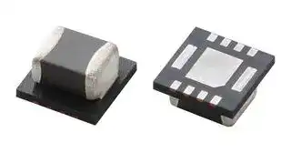
MYRGC075060B31RA
DC/DC POL Converter, Adjustable, Buck, 3 V to 36 V in, 1 V to 5 V out, 0.6 A out, 1.2 MHz, SMD-10
⚠️ Reference pricing provided. In case of supply shortages, we will connect you with our trusted procurement partners to ensure your project's continuity.
- Manufacturer: MURATA POWER SOLUTIONS
- Product type: DC / DC Non Isolated Board Mount Converters - Adjustable Output
- SVHC: No SVHC (07-Jul-2017)
- Depth: 3mm
- Width: 3mm
- Height: 1.7mm
- Product Range: PicoBK MYRGC-B Series
- Output Power Max: -
- Output Current Max: 600mA
- Output Voltage Max: 5V
- Output Voltage Min: 1V
- Input Voltage DC Max: 36V
- Input Voltage DC Min: 3V
- DC / DC Converter Type: Step Down, Module
- Power Supply Applications: Industrial, Household
- DC / DC Converter Output Type: Adjustable
| Delivery and price | |
|---|---|
| Units per pack | 100 |
| Price | 1.84 € |
| Current stock | 10+ |
| Lead time | 30 days |
Datasheet

## **“PicoBK™” MYRGC-W / MYRGC-B series**

## 36V, 600mA Inductor Built-in Step-down DC/DC Converter

## ■GENERAL DESCRIPTION

MYRGC075060W31RA and MYRGC075060B31RA

are small (3.0mm×3.0mm, h=1.7mm) 36V, 600mA step-down DC/DC converter with an integrated  control IC and coil. Integrating the coil makes for easier circuit board layout and minimizes malfunction and noise from the  component and wiring layout.

The input voltage range is 3.0 to 36V, the switching frequency is 1.2MHz, and a synchronous rectification circuit is used to achieve  a stable power supply at high efficiency. MYRGC075060W31RA fixes the operation frequency using PWM control to suppress output ripple voltage.

MYRGC075060B31RA automatically switches between PWM and PFM control to reduce loss by lowering the operation frequency  during low loads to achieve high efficiency across the entire range from low to high loads.

A 0.75V standard voltage supply is built in, and the output voltage can be set to 1.0V to 5.0V using an external resistance.

The soft start time is internally set to 2.0ms, and a time that is longer than the internal soft-start can be freely set depending on the  resistance and capacity connected to the EN/SS pin.

An overcurrent protection function and thermal shutdown function are built in as protective functions to ensure safe use in the  event of a short circuit.

## ■APPLICATIONS

- ●Electricity Meters

- ●Gas Detectors

- ●Various Sensors

- ●Industrial Equipment

- ●HomeAppliances

## ■FEATURES

Input Voltage Range : 3.0V ~ 36V (Absolute Max 40V) Output Voltage Range : 1.0V ~5.0V FB Voltage : 0.75V ± 1.5% Output Current : 600mA Oscillation Frequency : 1.2MHz Efficiency : 86%(VIN=12V,VOUT=5V, IOUT=300mA) Control Methods : PWM control(MYRGC075060W31RA) : PWM/PFM Auto(MYRGC075060B31RA) Function : Soft-start External settings Power good Over Current Protection Protection Circuits : (Automatic recovery) Thermal Shutdown Output Capacitor : Ceramic Capacitor Operating Ambient : -40 `℃` ~ `+` 105 `℃` Temperature Environmentally Friendly : EU RoHS Compliant, Pb Free Halogen Free

## ■TYPICAL APPLICATION CIRCUIT

**==> picture [215 x 75] intentionally omitted <==**

**----- Start of picture text -----**<br>
RPG<br>Lx L1<br>PG PG<br>VEN/SS EN/SS<br>L2 VOUT<br>VIN VIN CFB RFB1 CL<br>CIN1 CIN2 FB<br>GND RFB2<br>**----- End of picture text -----**<br>


## ■TYPICAL PERFORMANCE CHARACTERISTICS

**==> picture [221 x 195] intentionally omitted <==**

**----- Start of picture text -----**<br>
MYRGC075060W31RA / MYRGC075060B31RA<br>VIN=VEN/SS=12V, VOUT=5.0V<br>CIN1=4.7μF, CIN2=0.1μF, CL=22μF<br>100<br>90<br>80<br>70 7Zarn ae<br>60 /<br>50<br>40 f<br>MYRGC075060W31RA<br>30<br>20 / MYRGC075060B31RA<br>;<br>10 TA<br>0<br>0.1 1 10 100 1000<br>Output current : IOUT [mA]<br>Efficiency : EFFI [%]<br>**----- End of picture text -----**<br>


Export Control Code : X0863, Document No : D90DH - 00066

MYRGC-W/B series A01 Page 1 of 37

## **“PicoBK™” MYRGC-W / MYRGC-B series**

## 36V, 600mA Inductor Built-in Step-down DC/DC Converter

IN ELECTRONICS BLOCK DIAGRAM ~~ee~~ |

## ■BLOCK DIAGRAM

**==> picture [419 x 421] intentionally omitted <==**

**----- Start of picture text -----**<br>
L2 L1<br>Inductor<br>i] I<br>VIN<br>Local<br>Reg<br>Each<br>Circuit<br>Under Gate<br>Lock OutVoltage CLAMP<br>Current<br>SENSE<br>Thermal Operation Each<br>Shutdown Enable Circuit<br>CE<br>EN/SS Controller<br>Logic<br>Current Current<br>Vref Current<br>Feed Limit<br> Soft Start Limit<br>Back PFM<br>Hig h<br>Side<br>Buffer<br>PWM/PFM<br>FB Controller Lx<br>Logic Low<br>er Error PWM e Side<br> Amp. Comparator Buffe r<br>Ramp Wave _ Oscillator _<br>Generator<br>PG XxX] = < I x ] GND<br>Power-Good<br>Comparator<br>**----- End of picture text -----**<br>


- "PWM/PFM Controller Logic" in the MYRGC075060W31RA is fixed to PWM control.

- "PWM/PFM Controller Logic" In the MYRGC075060B31RA is fixed to PWM/PFM automatic switching control. Diodes inside the circuit are an ESD protection diode and a parasitic diode.

MYRGC-W/B series A01 Page 2 of 37

**“PicoBK™” MYRGC-W / MYRGC-B series MYRGC-W/MYRGC-** INNOVATOR **B Series** IN ELECTRONICS 36V, 600mA Inductor Built-in Step-down DC/DC Converter

## ■PIN CONFIGURATION

**==> picture [198 x 157] intentionally omitted <==**

**----- Start of picture text -----**<br>
9 L1<br>VIN 8 | | |__| 1 Lx<br>NC 7 | | || 2 GND<br>EN/SS 6 | | || 3 NC<br>PG 5 | | || 4 FB<br>10 L2<br>( BOTTOM VIEW )<br>**----- End of picture text -----**<br>


* The dissipation pad for the package should be solder plated in recommended mount pattern and metal masking so as to enhance mounting strength and heat release. If the pad needs to be connected to other pins, it should be connected to the GND (No.2) pin.

## ■PINASSIGNMENT

|PIN NUMBER|PINNAME|FUNCTION|
|---|---|---|
|1|LX|SwitchingOutput|
|2|GND|Ground|
|3|NC|No Connection|
|4|FB|Output Voltage Sense|
|5|PG|Power good Output|
|6|EN/SS|Enable Soft-start|
|7|NC|No Connection|
|8|VIN|PowerInput|
|9|L1|Inductor Electrodes|
|10|L2|Inductor Electrodes|


* The NC terminals (pin numbers 3 & 7) are not connected to the IC chip.

MYRGC-W/B series A01 Page 3 of 37

**“PicoBK™” MYRGC-W / MYRGC-B series** 36V, 600mA Inductor Built-in Step-down DC/DC Converter

|PINNAME|SIGNAL|STATUS|
|---|---|---|
|EN/SS|H|Active|
||L|Stand-by|
||OPEN|Undefined State(*1)|


> (*1) Please do not leave the EN/SS pin open. Each should have a certain voltage

|PINNAME|CONDITION|CONDITION|SIGNAL|
|---|---|---|---|
|PG|EN/SS = H|VFB> VPGDET|H (High impedance)|
|||VFB≦VPGDET|L (Low impedance)|
|||Thermal Shutdown|L (Low impedance)|
|||UVLO<br>(VIN< VUVLOD)|Undefined State|
||EN/SS = L|Stand-by|L (Low impedance)|


## ■ABSOLUTE MAXIMUM RATINGS

|PARAMETER|SYMBOL|RATINGS|UNITS|
|---|---|---|---|
|VINPin Voltage|VIN|-0.3 ~ +40|V|
|EN/SS Pin Voltage|VEN/SS|-0.3 ~ +40|V|
|FB Pin Voltage|VFB|-0.3 ~ +6.2|V|
|PG Pin Voltage|VPG|-0.3 ~ +6.2|V|
|PG Pin Current|IPG|8|mA|
|Lx PinVoltage|VLx|-0.3 ~ VIN+0.3 or +40 (*1)|V|
|Power Dissipation (Ta=25℃)|Pd|1950 (JESD51-7 board) (*2)|mW|
|Operating Ambient Temperature|Topr|-40 ~+105|℃|
|Storage Temperature|Tstg|-55 ~+125|℃|


All voltages are described based on the GND pin.

> (*1) The maximum value should be either VIN+0.3V, or 40V, whichever is the lowest.

(*2) The power dissipation figure shown is PCB mounted and is for reference only.

MYRGC-W/B series A01 Page 4 of 37

## **“PicoBK™” MYRGC-W / MYRGC-B series**

## 36V, 600mA Inductor Built-in Step-down DC/DC Converter

## ■ELECTRICAL CHARACTERISTICS

MYRGC075060W31RA / MYRGC075060B31RA

Ta=25 `℃`

**==> picture [480 x 529] intentionally omitted <==**

**----- Start of picture text -----**<br>
|||||||||||||||
|---|---|---|---|---|---|---|---|---|---|---|---|---|---|
|PARAMETER|SYMBOL|CONDITIONS|MIN.|TYP.|MAX.|UNIT|CIRCUIT|
|VFB=0.739V→0.761V,|
|FB Voltage|VFBE|FB Voltage when Lx pin voltage changes|0.739|0.750|0.761|V|②|
|from"H" level to "L" level|
|Output Voltage|
|Setting Range|[(*1)]|VOUTSET|-|1.0|-|5.0|V|-|
|Input Voltage|
|Operating Range|[(*1)]|VIN|-|3.0|-|36.0|V|-|
|VEN/SS=12V,VIN=2.8V|
|Ta=25|℃|2.6|2.7|2.8|
|→  2.6V,VFB=0V|
|UVLO Detect Voltage|VUVLOD|VIN Voltage which Lx|V|②|
|Ta=-40~105|℃|[(*2)]|2.53|-|2.87|
|pin  voltage holding "H"|
|level|
|VEN/SS=12V,VIN=2.7V|
|Ta=25|℃|2.7|2.8|2.9|
|→  2.9V,VFB=0V|
|UVLO Release Voltage|VUVLOR|VIN Voltage which Lx|V|②|
|Ta=-40~105|℃|[(*2)]|2.63|-|2.97|
|pin  voltage holding "L"|
|level|
|Quiescent Current|
|(MYRGC075060W31RA)|Iq|VFB=0.825V|-|180|350|μA|④|
|Quiescent Current|
|(MYRGC075060B31RA)|Iq|VFB=0.825V|-|12.5|21.0|μA|④|
|Stand-by Current|ISTBY|VIN=12V,VEN/SS=VFB=0V|-|1.65|2.50|μA|④|
|Connected to external components,|
|Oscillation Frequency|fOSC|IOUT=150mA|1.098|1.200|1.302|MHz|①|
|Minimum On Time|tONMIN|Connected to external components|-|85|[(*1)]|-|ns|①|
|Minimum Duty Cycle|DMIN|VFB=0.825V|-|-|0|%|②|
|Maximum Duty Cycle|DMAX|VFB=0.675V|100|-|-|%|②|
|Lx SW "H" On Resistance|RLxH|VFB=0.675V,ILx=200mA|-|1.20|1.38|Ω|⑤|
|Lx SW "L" On Resistance|RLxL|-|0.60|[(*1)]|-|Ω|-|
|High side Current Limit|[(*2)]|ILIMH|VFB=VFBE×0.98|1.0|1.3|-|A|⑤|
|Internal Soft-Start Time|tSS1|VFB=0.675V|1.6|2.0|2.4|ms|②|
|External Soft-Start Time|tSS2|VFB=0.675V|21|26|33|ms|③|
|RSS=430kΩ, CSS=0.47μF|
|PFM Switch Current|IPFM|Connected to external components,|-|450|-|mA|①|
|(MYRGC075060B31RA)|VIN=VEN/SS=12V|、|IOUT=1mA|
|Efficiency|EFFI|Connected to external components,|-|86|-|%|①|
|VIN=12V, VOUT=5V, IOUT=300mA|
|FB Voltage  Temperature|ΔVFB/|
|Characteristics|(ΔTopr・VFBE)|-40|℃≦|Topr|≦|105|℃|-|±100|-|ppm/|℃|②|

**----- End of picture text -----**<br>


Test Condition: Unless otherwise stated, VIN=12V, VEN/SS=12V, PG=OPEN

Peripheral parts connection conditions (VOUT=5.0V): RFB1=680kΩ, RFB2=120kΩ, CFB=15pF, CL=22μF, CIN=4.7μF

> (*1) Design reference value. This parameter is provided only for reference.

(*2) Current limit denotes the level of detection at peak of coil current.

MYRGC-W/B series A01 Page 5 of 37

## **“PicoBK™” MYRGC-W / MYRGC-B series** 36V, 600mA Inductor Built-in Step-down DC/DC Converter

## MYRGC075060W31RA / MYRGC075060B31RA

Ta=25℃

|PARAMETER|SYMBOL|CONDITIONS|CONDITIONS|MIN.|TYP.|MAX.|UNIT|CIRCUIT|
|---|---|---|---|---|---|---|---|---|
|PG Detect Voltage|VPGDET|VFB=0.712V→0.638V,<br>RPG:100kΩ pull-up to 5V<br>FB Voltage when PG pin voltage changes<br>from"H" level to "L" level||0.638|0.675|0.712|V|⑤|
|PG Output Voltage|VPG|VFB=0.6V,IPG=1mA||-|-|0.3|V|②|
|FB "H" Current|IFBH|VIN=VEN/SS=36V, VFB=3.0V||-0.1|0.0|0.1|μA|④|
|FB "L" Current|IFBL|VIN=VEN/SS=36V, VFB=0V||-0.1|0.0|0.1|μA|④|
|EN/SS "H" Voltage|VEN/SSH|VEN/SS=0.3V→2.5<br>V,  VFB=0.71V<br>EN/SS Voltage when Lx<br>pin voltage changes from<br>"L" level to "H"level|Ta=25℃|2.5|-|36.0|V|②|
||||Ta=-40~105℃(*1)||||||
|EN/SS "L" Voltage|VEN/SSL|VEN/SS=2.5V→0.3<br>V,  VFB=0.71V<br>EN/SS Voltage when Lx<br>pin voltage changes from<br>"H" level to "L"level|Ta=25℃|GND|-|0.3|V|②|
||||Ta=-40~105℃(*1)||||||
|EN/SS "H" Current|IEN/SSH|VIN=VEN/SS=36V, VFB=0.825V||-|0.1|0.3|μA|④|
|EN/SS "L" Current|IEN/SSL|VIN=36V, VEN/SS=0V, VFB=0.825V||-0.1|0.0|0.1|μA|④|
|Thermal Shutdown<br>Temperature|TTSD|Junction Temperature||-|150|-|℃|-|
|Thermal Shutdown<br>HysteresisWidth|THYS|Junction Temperature||-|25|-|℃|-|
|Inductance|L|Test Freq.=1MHz||-|4.7|-|μH|-|
|Inductor Rated Current|IDC|⊿T=+40℃||-|1.8|-|A|-|


Test Condition: Unless otherwise stated, VIN=12V, VEN/SS=12V, PG=OPEN

(*1) Design reference value. This parameter is provided only for reference.

MYRGC-W/B series A01 Page 6 of 37

## **“PicoBK™” MYRGC-W / MYRGC-B series**

## 36V, 600mA Inductor Built-in Step-down DC/DC Converter

## ■TEST CIRCUITS

Circuit No.①

**==> picture [346 x 128] intentionally omitted <==**

**----- Start of picture text -----**<br>
Probe<br>VIN<br>A L2<br>C) /<br>EN/SS<br>L1<br>@ V CIN Lx VOUT<br>V<br>PG CFB RFB1 A<br>©) @<br>FB CL<br>V<br>GND RFB2<br>lo 3 ral<br>**----- End of picture text -----**<br>


Circuit No. `②`

**==> picture [339 x 111] intentionally omitted <==**

**----- Start of picture text -----**<br>
VIN<br>L2<br>@ V EN/SS alae Probe<br>L1 eo<br>o<br>CIN V RPG=100kΩ Lx<br>(—) OG O PG<br>FB<br>V<br>V<br>7 GND V @<br>100kΩ<br>—I¢<br>**----- End of picture text -----**<br>


Circuit No. `③`

**==> picture [341 x 104] intentionally omitted <==**

**----- Start of picture text -----**<br>
VIN<br>L2<br>RSS=430kΩ rcccct Probe<br>EN/SS L1 ~r---t<br>4<br>CIN Lx o<br>V<br>©) OC V CSS PG<br>FB<br>0.47μF OC V<br>GND @ V 100kΩ<br>**----- End of picture text -----**<br>


MYRGC-W/B series A01 Page 7 of 37

**“PicoBK™” MYRGC-W / MYRGC-B series** 36V, 600mA Inductor Built-in Step-down DC/DC Converter

Circuit No. `④`

**==> picture [258 x 95] intentionally omitted <==**

**----- Start of picture text -----**<br>
VIN<br>L2<br>A EN/SS<br>L1<br>A<br>Lx<br>V<br>V<br>PG<br>FB<br>A<br>GND V<br>**----- End of picture text -----**<br>


Circuit No. `⑤`

**==> picture [284 x 127] intentionally omitted <==**

**----- Start of picture text -----**<br>
VIN<br>L2<br>V<br>EN/SS<br>L1<br>CIN V RPG=100kΩ Lx<br>PG<br>FB<br>V<br>V<br>GND V<br>Probe<br>**----- End of picture text -----**<br>


MYRGC-W/B series A01 Page 8 of 37

## **“PicoBK™” MYRGC-W / MYRGC-B series**

## 36V, 600mA Inductor Built-in Step-down DC/DC Converter

## ■TYPICAL APPLICATION CIRCUIT / Parts Selection Method

**==> picture [216 x 75] intentionally omitted <==**

**----- Start of picture text -----**<br>
RPG<br>Lx L1<br>PG PG<br>VEN/SS EN/SS<br>L2 VOUT<br>VIN VIN CFB RFB1 CL<br>CIN1 CIN2 FB<br>GND RFB2<br>**----- End of picture text -----**<br>


* The inductor is dedicated to this product. Please do not use it for purposes other than this product.

## `【` Typical Example `】`

||VALUE|
|---|---|
|CIN1(*1)|50V/4.7μF|
|CIN2|50V/0.1μF|
|CL(*2)|10V/10μF|
||35V/10μF|
||25V/22μF|


Select parts considering the DC bias characteristics and rated voltage of ceramic capacitors.

- (*1) For CIN1, use a capacitor with the same or higher effective capacity value as the recommended components.

- (*2) For CL, use a capacitor with the same or higher effective capacity value as the recommended components. If a capacitor with a low effective capacity value is used, the output voltage may become unstable. However, if large capacity capacitors, such as electrolytic capacitors, are connected in parallel, the inrush current during startup could increase or the output could become unstable.

MYRGC-W/B series A01 Page 9 of 37

## **“PicoBK™” MYRGC-W / MYRGC-B series** 36V, 600mA Inductor Built-in Step-down DC/DC Converter

## ■TYPICAL APPLICATION CIRCUIT / Parts Selection Method (Continued)

< Output Voltage Setting Value VOUTSET Setting >

The output voltage can be set by adding an external dividing resistor.

The output voltage is determined by the equation below based on the values of RFB1 and RFB2.

VOUTSET = 0.75V × (RFB1 + RFB2) / RFB2 With RFB2 `≦` 200kΩ and RFB1 + RFB2 `≦` 1MΩ

< CFB Setting >

Adjust the value of the phase compensation speed-up capacitor CFB using the equation below.

**==> picture [95 x 57] intentionally omitted <==**

## 【Setting Example】

When the output voltage setting is 5V with fosc=1.2MHz, CL=22μF, L=4.7μH,

VOUTSET = 0.75V × (680kΩ + 120kΩ) / 120kΩ = 5.0V,

From the above formula, fzfb = 15.66kHz is targeted,

CFB= 1 / (2 × π × 15.66kHz × 680kΩ) = 14.95pF, which is 15pF for the E24 series.

|VOUTSET|RFB1|RFB2|CFB|Target fzfb|
|---|---|---|---|---|
|1.2V|120kΩ|200kΩ|82pF|15.66kHz|
|3.3V|510kΩ|150kΩ|22pF|15.66kHz|
|5.0V|680kΩ|120kΩ|15pF|15.66kHz|


MYRGC-W/B series A01 Page 10 of 37

## **“PicoBK™” MYRGC-W / MYRGC-B series**

## 36V, 600mA Inductor Built-in Step-down DC/DC Converter

## ■OPERATIONAL EXPLANATION

The MYRGC075060W31RA / MYRGC075060B31RA consist internally of a reference voltage supply with soft-start function, a ramp wave circuit, an  error amp, a PWM comparator, a High side driver FET, a Low side driver FET, a High side buffer circuit, a Low side buffer circuit,  a current sense circuit, a phase compensation (Current feedback) circuit, a current limiting circuit, an under voltage lockout  (UVLO) circuit, an internal power supply (Local Reg) circuit, a gate clamp (CLAMP) circuit and other elements. The control method is the current mode control method for handling low ESR ceramic capacitors.

**==> picture [383 x 378] intentionally omitted <==**

**----- Start of picture text -----**<br>
L2 L1<br>Inductor<br>VIN<br>Local<br>Reg<br>Each<br>Circuit<br>- Lock OutVoltageUnder Current CLAMPGate<br>SENSE<br>Thermal Operation Each a<br>Shutdown Enable Circuit<br>CE<br>EN/SS E Controller<br>Logic<br>Current Current<br>Vref Current<br> Soft Start FeedBack Limit LimitPFM<br>Hig h<br>Side<br>Buffer<br>@®) © PWM/PFM<br>FB Controller Lx<br>e Error o PWM Logic SideLow i<br> Amp. Comparator Buffe r<br>Ha<br>Ramp Wave Oscillator<br>Generator<br>PG<br>xX x X GND<br>K-<C<br>Power-Good<br>Comparator<br>**----- End of picture text -----**<br>


MYRGC-W/B series A01 Page 11 of 37

## **“PicoBK™” MYRGC-W / MYRGC-B series** muRata a 36V, 600mA Inductor Built-in Step-down DC/DC Converter

## ■OPERATIONAL EXPLANATION (Continued)

## < Normal Operation >

The standard voltage Vref and FB pin voltage are compared using an error amplifier and then the control signal to which phase compensation has been added to the error amplifier output is input to the PWM comparator. The PWM comparator compares the above control signal and lamp wave to control the duty width during PWM control. Continuously conducting these controls stabilizes the output voltage.

In addition, the current detecting circuit monitors the driver FET current for each switching and modulates the error amplifier output signal into a multiple feedback signal (current feedback circuit). This achieves stable feedback control even when low ESR capacitors, such as ceramic capacitors, are used to stabilize the output voltage.

## MYRGC075060W31RA

The MYRGC075060W31RA (PWM control) performs switching at a set switching frequency fOSC regardless of the output current. At light  loads the on time is short and the circuit operates in discontinuous mode, and as the output current increases, the on time becomes  longer and the circuit operates in continuous mode.

**==> picture [461 x 130] intentionally omitted <==**

**----- Start of picture text -----**<br>
fOSC fOSC<br>tON tON<br>Lx Lx<br>0V 0V<br>Coil  IOUT<br>Current Coil<br>Current<br>IOUT<br>0mA 0mA<br>**----- End of picture text -----**<br>


**==> picture [11 x 61] intentionally omitted <==**

**----- Start of picture text -----**<br>
0V<br>0mA<br>**----- End of picture text -----**<br>


**==> picture [179 x 8] intentionally omitted <==**

**----- Start of picture text -----**<br>
MYRGC075060W31RA: Example of light load operation<br>**----- End of picture text -----**<br>


**==> picture [184 x 8] intentionally omitted <==**

**----- Start of picture text -----**<br>
MYRGC075060W31RA: Example of heavy load operation<br>**----- End of picture text -----**<br>


## MYRGC075060B31RA

The MYRGC075060B31RA (PWM/PFM automatic switching control) lowers the switching frequency during light loads by turning on the  High side driver FET when the coil current reaches the PFM current (IPFM). This operation reduces the loss during light loads and  achieves high efficiency from light to heavy loads. As the output current increases, the switching frequency increases proportional  to the output current, and when the switching frequency increases fOSC, the circuit switches from PFM control to PWM control and  the switching frequency becomes fixed.

**==> picture [218 x 115] intentionally omitted <==**

**----- Start of picture text -----**<br>
tON<br>Lx<br>0V<br>IPFM<br>Coil<br>Current<br>IOUT 0mA<br>MYRGC075060B31RA: Example of light load operation<br>**----- End of picture text -----**<br>


**==> picture [221 x 148] intentionally omitted <==**

**----- Start of picture text -----**<br>
fOSC<br>tON<br>Lx<br>0V<br>IOUT<br>Coil<br>Current<br>0mA<br>MYRGC075060B31RA: Example of heavy load operation<br>**----- End of picture text -----**<br>


## < 100% Duty Cycle Mode >

When the dropout voltage is low or there is a transient response, the circuit might change to the 100% Duty cycle mode where the High side driver FET is continuously on.

The 100% Duty cycle mode operation makes it possible to maintain the output current even when the dropout voltage is low such as when the input voltage declines due to cranking, etc.

MYRGC-W/B series A01 Page 12 of 37

## **“PicoBK™” MYRGC-W / MYRGC-B series**

## 36V, 600mA Inductor Built-in Step-down DC/DC Converter

## ■OPERATIONAL EXPLANATION (Continued)

## < CE Function >

When an “H” voltage (VEN/SSH) is input to the EN/SS pin, normal operation is performed after the output voltage is started up by the soft start function, normal operation is performed. When the “L” voltage (VEN/SSL) is input to the EN/SS pin, the circuit enters the standby state, the supply current is suppressed to the standby current ISTB (TYP.165 μA), and the High side driver FET and Low side driver FET are turned off.

## < Soft Start Function>

This function gradually starts up the output voltage to suppress the inrush current.

The soft start time is the time until the output voltage from VEN/SSH reaches 90% of the output voltage set value, and when the output voltage increases further, the soft start function is cancelled to switch to normal operation.

## Internal Soft Start Time

The internal soft start time (tSS1) is configured so that after the “H” voltage (VEN/SSH) is input to the EN/SS pin, the standard voltage connected to the error amplifier increases linearly during the soft-start period. This causes the output voltage to increase proportionally to the standard voltage increase. This operation suppresses the inrush current and smoothly increases the output voltage.

**==> picture [365 x 70] intentionally omitted <==**

**----- Start of picture text -----**<br>
tss1 tss1<br>EN/SS V1<br>V1<br>90% of setting voltage<br>VOUT<br>**----- End of picture text -----**<br>


< Internal soft start EN/SS circuit >

**==> picture [91 x 6] intentionally omitted <==**

**----- Start of picture text -----**<br>
< Overview of internal soft start ><br>**----- End of picture text -----**<br>


## External Setting Soft Start Time

The external setting soft start time (tSS2) can adjust the increase speed of the standard voltage in the IC by adjusting the EN/SS pin voltage inclination during startup using externally connected component RSS and CSS. This makes it possible to externally adjust the soft start time.

Soft start time (tSS2) is approximated by the equation below according to values of V1, RSS, and CSS When tss2 is shorter than tss1, the output voltage rises at the internal soft start time.

tss2=Css×Rss× ln ( V1 / (V1-1.45V) )

## 【Setting Example】

CSS = 0.47μF, RSS = 430kΩ, V1 = 12V

tSS2 = 0.47μF x 430kΩ x ( ln (12V/(12V-1.45V)) = 26ms

**==> picture [406 x 97] intentionally omitted <==**

**----- Start of picture text -----**<br>
RSS tss2<br>EN/SS<br>V1<br>V1 CSS<br>1.45V<br>EN/SS<br>90% of setting voltage<br>VOUT<br>**----- End of picture text -----**<br>


**==> picture [98 x 6] intentionally omitted <==**

**----- Start of picture text -----**<br>
< External soft start EN/SS circuit ><br>**----- End of picture text -----**<br>


**==> picture [93 x 6] intentionally omitted <==**

**----- Start of picture text -----**<br>
< Overview of external soft start ><br>**----- End of picture text -----**<br>


MYRGC-W/B series A01 Page 13 of 37

## **“PicoBK™” MYRGC-W / MYRGC-B series** 36V, 600mA Inductor Built-in Step-down DC/DC Converter

## ■OPERATIONAL EXPLANATION (Continued)

## < Power Good >

The output state can be monitored using the power good function. The PG pin is an Nch open drain output, therefore a pull-up resistor (approx. 100kΩ) must be connected to the PG pin.

The pull-up voltage should be 5.5V or less. When not using the power good function, connect the PG terminal to GND or leave  it open.

|CONDITION|CONDITION|SIGNAL|
|---|---|---|
|EN/SS = H|VFB> VPGDET|H (High impedance)|
||VFB≦VPGDET|L (Low impedance)|
||Thermal Shutdown|L (Low impedance)|
||UVLO (VIN< VUVLOD)|Undefined State|
|EN/SS = L|Stand-by|L (Low impedance)|


## < UVLO Function >

When the VIN pin voltage falls below VUVLOD (TYP. 2.7V), the high side driver FET and low side driver FET are forcibly turned off to prevent false pulse output due to instable operation of the internal circuits. When the VIN pin voltage rises above VUVLOR (TYP. 2.8V), the UVLO function is released, the soft start function activates, and output start operation begins. Stopping by UVLO is not shutdown; only pulse output is stopped and the internal circuits continue to operate.

## < Thermal Shutdown Function >

A thermal shutdown (TSD) function is built in for protection from overheating.When the junction temperature reaches the thermal shutdown detection temperature TTSD, the High side driver FET and Low side driver FET are compulsorily turned off.

If the driver FET continues in the off state, the junction temperature declines, and when the junction temperature falls to the thermal shutdown cancel temperature, the thermal shutdown function is cancelled and the soft-start function operates to start up the output voltage.

MYRGC-W/B series A01 Page 14 of 37

## **“PicoBK™” MYRGC-W / MYRGC-B series**

## 36V, 600mA Inductor Built-in Step-down DC/DC Converter

## ■OPERATIONAL EXPLANATION (Continued)

## < Current Limit Function >

The current limiting circuit of the MYRGC075060W31RA / MYRGC075060B31RA monitors the current that flows through the High side driver FET and  Low side driver FET, and when over current is detected, the current limiting function activates.

## `①` High side driver FET current limiting

The current in the High side driver FET is detected to equivalently monitor the peak value of the coil current. The High side driver FET current limiting function forcibly turns off the High side driver FET when the peak value of the coil current reaches the High side driver current limit value ILIMH.

High side driver FET current limit value ILIMH=1.3A(TYP.)

## `②` Low side driver FET current limiting

The current in the Low side driver FET is detected to equivalently monitor the bottom value of the coil current. The Low side driver FET current limiting function operates when the High side driver FET current limiting value reaches ILIMH. The Low side driver FET current limiting function prohibits the High side driver FET from turning on in an over current state where the bottom value of the coil current is higher than the Low side driver FET current limit value ILIML.

Low side driver FET current limit value ILIML=0.9A(TYP.)

When the output current increases and reaches the current limit value, the current foldback circuit operates and lowers the output voltage and FB voltage. The ILIMH and ILIML decline accompanying the FB voltage decrease to restrict the output current. When the overcurrent state is removed, the foldback circuit operation increases the ILIMH and ILIML together with output voltage  to return the output to the output voltage set value.

**==> picture [431 x 189] intentionally omitted <==**

**----- Start of picture text -----**<br>
> Current Limit<br>IILIMHLIML=0.9A(TYP.)=1.3A(TYP.) oe pNAAALMOUNDS\ NIL NL NJ\Se eee o-oo nnn nn gg eee eee<br>Coil  |I\Noo ON [| _---. _o---e<br>Current a 0A<br>Lx<br>0V<br>VOUT ee|I<br>| |<br>--------------~~, ----- 0V<br>| |<br>RLOAD ee ee<br>a 0Ω<br>**----- End of picture text -----**<br>


MYRGC-W/B series A01 Page 15 of 37

## **“PicoBK™” MYRGC-W / MYRGC-B series** 36V, 600mA Inductor Built-in Step-down DC/DC Converter

## ■NOTES ON USE

- 1)    In the case of a temporary and transient voltage drop or voltage rise.

If the absolute maximum ratings are exceeded, the IC may deteriorate or be destroyed.

If a voltage exceeding the absolute maximum voltage is applied to the IC due to chattering caused by a mechanical switch or an external surge voltage, please use a protection element such as a TVS and a protection circuit as a countermeasure.

**==> picture [240 x 81] intentionally omitted <==**

**----- Start of picture text -----**<br>
RPG<br>Lx L1<br>PG PG<br>VEN/SS EN/SS<br>L2 VOUT<br>VIN 'i CIN1 CIN2 VIN FB CFB RFB1 CL<br>TVS GND<br>RFB2<br>**----- End of picture text -----**<br>


When the input voltage decreases below the output voltage, there is a possibility that an overcurrent will flow in the IC’s internal parasitic diode and Lx pin. If the current is pulled into the input side by the low impedance between VIN-GND, then countermeasures, such as adding an SBD between VOUT-VIN, should be taken.

**==> picture [372 x 121] intentionally omitted <==**

**----- Start of picture text -----**<br>
SBD<br>aie - See f<br>\ [f]<br>\ f<br>' [1]<br>' '<br>'<br>i\ RPG ['] '<br>Lx L1<br>'\ PG PG [']<br>VEN/SS \ EN/SS f\<br>\' L2 VOUT<br>'<br>i<br>VIN CIN1 \ CIN2 VIN FB CFB RFB1 CL<br>GND<br>RFB2<br>**----- End of picture text -----**<br>


When a negative voltage is applied to the input voltage by a reverse connection or chattering, an overcurrent could flow in the IC’s parasitic diode and damage the IC. Take countermeasures, such as adding a reverse touching protection diode.

**==> picture [246 x 83] intentionally omitted <==**

**----- Start of picture text -----**<br>
RPG<br>Lx L1<br>PG PG<br>VEN/SS EN/SS<br>Reverse Touching L2 VOUT<br>Protection Diode<br>VIN VIN CFB RFB1 CL<br>FB<br>CIN1 CIN2 GND<br>RFB2<br>**----- End of picture text -----**<br>


MYRGC-W/B series A01 Page 16 of 37

## **“PicoBK™” MYRGC-W / MYRGC-B series**

## 36V, 600mA Inductor Built-in Step-down DC/DC Converter

## ■NOTES ON USE (Continued)

- 2) Make sure that the absolute maximum ratings of the external components and of this IC are not exceeded.

- 3) The DC/DC converter characteristics depend greatly on the externally connected components as well as on the characteristics of this IC, so refer to the specifications and standard circuit examples of each component when carefully considering which components to select.

   - Be especially careful of the capacitor characteristics and use X7R or X5R (EIA standard) ceramic capacitors.

   - The capacitance decrease caused by the bias voltage may become large depending on the external size of the capacitor.

- 4) The current limit value is the coil current peak value when switching is not conducted. The coil current peak value when the actual current limit function begins to operate may exceed the current limit of the

- electrical characteristics due to the effect of the propagation delay inside the circuit.

- 5) When the On time is less than the Min On Time (tONMIN) and the dropout voltage is large or the load is low, the PWM control operates intermittently and the ripple voltage may become large or the output voltage may become unstable.

- 6) The ripple voltage could be increased when switching from discontinuous conduction mode to continuous conduction mode and when switching to 100% Duty cycle.

- 7) The PWM/PFM auto series may cause superimposed ripple voltage by continuous pulses if used in high temperature and  no load conditions. It is necessary to set an idle current of higher than 100μA from VOUT if used at no load. It can have the same effect as when RFB2 is lower than 7.5kΩ. Please refer to the

   - < Output Voltage Setting Value VOUTSET Setting > section under TYPICAL APPLICATION CIRCUIT.

- 8) If the voltage at the EN/SS Pin does not start from 0V but is at the midpoint potential when the power is switched on, the  soft start function may not work properly and it may cause larger inrush current and bigger ripple voltages.

- 9) Murata places an importance on improving our products and their reliability. We request that users incorporate fail safe designs and post aging protection treatment when using Murata products in their systems.

MYRGC-W/B series A01 Page 17 of 37

## **“PicoBK™” MYRGC-W / MYRGC-B series**

## 36V, 600mA Inductor Built-in Step-down DC/DC Converter

## ■NOTES ON USE (Continued)

- 10) Pattern Layout Instructions

   - (1) The operation may become unstable due to noise and/or phase lag from the output current when the wire impedance is high. Please place the input capacitor (CIN1, CIN2) and the output capacitor (CL) as close to the IC as possible.

   - (2)     In order to stabilize the VIN voltage level, we recommend that a bypass capacitor (CIN1, CIN2) be connected as close as possible to the VIN and GND pins.

   - (3)      Please mount each external component as close to the IC as possible.

   - (4)      Wire external components as close to the IC as possible and use thick, short connecting traces to reduce the circuit impedance.

   - (5)      Make sure that the GND traces are as thick as possible, as variations in ground potential caused by high ground currents at the time of switching may result in instability of the IC.

   - (6) This product has a built in driver FET, which causes heatgeneration from the on resistance, so take measures to dissipate  the heat whennecessary.

< Reference Pattern Layout >

**==> picture [211 x 9] intentionally omitted <==**

**----- Start of picture text -----**<br>
< Layer1 > < Layer2 ><br>**----- End of picture text -----**<br>


**==> picture [211 x 9] intentionally omitted <==**

**----- Start of picture text -----**<br>
< Layer3 > < Layer4 ><br>**----- End of picture text -----**<br>


MYRGC-W/B series A01 Page 18 of 37

## **“PicoBK™” MYRGC-W / MYRGC-B series**

## 36V, 600mA Inductor Built-in Step-down DC/DC Converter

## ■HANDLING OF THIS PRODUCT

- (1)The coil complies with the general surface-mounted type chip coil (inductor) specifications and could have scratches, be dirty with flux, etc.

- (2) Please do not use this product in the following environments: Areas where it could come in to contact with water or salt water. Areas where it could be affected by condensation. Areas where it could come in contact with toxic gases (Hydrogen Sulfide, Sulfurous Acid, Chlorine, Ammonia, etc.)

- (3) This product should not be washed in a solvent.

## ■ABOUT IMPLEMENTATION

- (1) This product is only suitable for reflow soldering (it is not suitable for flow soldering).

- (2) This product uses solder to mount the coil on top of the package. This is no problem for regular circuit board mounted reflow, but if excessive impact is applied during reflow, the mounted coil could be moved out of position or the coil could fall off. Be careful not to strike the circuit board during circuit board mounting reflow.

MYRGC-W/B series A01 Page 19 of 37

## **“PicoBK™” MYRGC-W / MYRGC-B series**

## 36V, 600mA Inductor Built-in Step-down DC/DC Converter

## ■TYPICAL PERFORMANCE CHARACTERISTICS

(1) Efficiency vs. Output Current

**==> picture [188 x 157] intentionally omitted <==**

**----- Start of picture text -----**<br>
MYRGC075060W31RA<br>(VIN=12V, VOUT=3.3V)<br>CIN1=4.7μF, CIN2=0.1μF, CL=22μF<br>100<br>90 ee ee ee<br>80 ee ee ee<br>70 ee ee<br>60 a ee ee ee<br>50 es A ee<br>40 a ee Gee ee<br>3020 eea ee 2 ee<br>10 4 ae ee<br>0 Ce eee<br>0.1 1 10 100 1000<br>Output Current :IOUT[mA]<br>Efficiency :EFFI [%]<br>**----- End of picture text -----**<br>


**==> picture [120 x 29] intentionally omitted <==**

**----- Start of picture text -----**<br>
MYRGC075060W31RA<br>(VIN=12V, VOUT=5V)<br>CIN1=4.7μF, CIN2=0.1μF, CL=22μF<br>**----- End of picture text -----**<br>


**==> picture [184 x 122] intentionally omitted <==**

**----- Start of picture text -----**<br>
100<br>90 ee ee ee<br>80 rr ee<br>70 ee ee ee<br>60 ee es Ae<br>50 ee ee es ee<br>40 a<br>3020 Ae4ee<br>10 ee Ae ee ee<br>0 aee Aa eee eee<br>0.1 1 10 100 1000<br>Output Current :IOUT[mA]<br>Efficiency :EFFI [%]<br>**----- End of picture text -----**<br>


**==> picture [186 x 158] intentionally omitted <==**

**----- Start of picture text -----**<br>
MYRGC075060B31RA<br>(VIN=12V, VOUT=3.3V)<br>CIN1=4.7μF, CIN2=0.1μF, CL=22μF<br>100<br>90 ee ee ee<br>80 eee<br>70 a ee<br>60 [IZ |<br>50 rr a ee ee<br>40<br>30 ee ee ee ee<br>20 ee ee ee ee<br>10 po<br>0 Lo<br>0.1 1 10 100 1000<br>Output Current :IOUT[mA]<br>Efficiency :EFFI [%]<br>**----- End of picture text -----**<br>


MYRGC075060B31RA (VIN=12V, VOUT=5V) CIN1=4.7μF, CIN2=0.1μF, CL=22μF

**==> picture [184 x 122] intentionally omitted <==**

**----- Start of picture text -----**<br>
100<br>90<br>80<br>70<br>60<br>50<br>40<br>30<br>20<br>10<br>0<br>0.1 1 10 100 1000<br>Output Current :IOUT[mA]<br>Efficiency :EFFI [%]<br>**----- End of picture text -----**<br>


MYRGC-W/B series A01 Page 20 of 37

## **“PicoBK™” MYRGC-W / MYRGC-B series**

## 36V, 600mA Inductor Built-in Step-down DC/DC Converter

## ■TYPICAL PERFORMANCE CHARACTERISTICS (Continued)

(2) Output Voltage vs. Output Current

MYRGC075060W31RA (VIN=12V, VOUT=3.3V) CIN1=4.7μF, CIN2=0.1μF, CL=22μF

**==> picture [196 x 123] intentionally omitted <==**

**----- Start of picture text -----**<br>
3.6<br>3.5<br>3.4<br>3.3<br>3.2<br>3.1<br>3.0<br>0.1 1 10 100 1000<br>Output Current :IOUT[mA]<br> [V]<br>OUT<br>Output Voltage : V<br>**----- End of picture text -----**<br>


MYRGC075060W31RA (VIN=12V, VOUT=5V) CIN1=4.7μF, CIN2=0.1μF, CL=22μF

**==> picture [193 x 123] intentionally omitted <==**

**----- Start of picture text -----**<br>
5.3<br>5.2<br>5.1<br>5.0<br>4.9<br>4.8<br>4.7<br>0.1 1 10 100 1000<br>Output Current :IOUT[mA]<br> [V]<br>OUT<br>Output Voltage : V<br>**----- End of picture text -----**<br>


**==> picture [196 x 162] intentionally omitted <==**

**----- Start of picture text -----**<br>
MYRGC075060B31RA<br>(VIN=12V, VOUT=3.3V)<br>CIN1=4.7μF, CIN2=0.1μF, CL=22μF<br>3.6<br>3.5<br>3.4<br>3.3<br>3.2<br>3.1<br>3.0<br>0.1 1 10 100 1000<br>Output Current :IOUT[mA]<br>[V]<br>OUT<br>Output Voltage : V<br>**----- End of picture text -----**<br>


**==> picture [195 x 162] intentionally omitted <==**

**----- Start of picture text -----**<br>
MYRGC075060B31RA<br>(VIN=12V, VOUT=5V)<br>CIN1=4.7μF, CIN2=0.1μF, CL=22μF<br>5.3<br>5.2<br>5.1<br>5.0<br>4.9<br>4.8<br>4.7<br>0.1 1 10 100 1000<br>Output Current :IOUT[mA]<br>[V]<br>OUT<br>Output Voltage : V<br>**----- End of picture text -----**<br>


MYRGC-W/B series A01 Page 21 of 37

## **“PicoBK™” MYRGC-W / MYRGC-B series** 36V, 600mA Inductor Built-in Step-down DC/DC Converter

## ■TYPICAL PERFORMANCE CHARACTERISTICS (Continued)

(3) Ripple Voltage vs. Output Current

MYRGC075060W31RA (VIN=12V, VOUT=3.3V) CIN1=4.7μF, CIN2=0.1μF, CL=22μF

**==> picture [187 x 123] intentionally omitted <==**

**----- Start of picture text -----**<br>
100<br>90<br>80<br>70<br>60<br>50<br>40<br>30<br>20<br>10 —<——_|<br>0<br>0.1 1 10 100 1000<br>Output Current :IOUT[mA]<br>Ripple Voltage :Vr [mV]<br>**----- End of picture text -----**<br>


**==> picture [192 x 167] intentionally omitted <==**

**----- Start of picture text -----**<br>
MYRGC075060W31R<br>(VIN=12V, VOUT=5V)<br>CIN1=4.7μF, CIN2=0.1μF, CL=22μF<br>100<br>90<br>80<br>70<br>60<br>50<br>40<br>30<br>20<br>10<br>0<br>0.1 1 10 100 1000<br>Output Current :IOUT[mA]<br>Ripple Voltage :Vr [mV]<br>**----- End of picture text -----**<br>


**==> picture [189 x 164] intentionally omitted <==**

**----- Start of picture text -----**<br>
MYRGC075060B31RA<br>(VIN=12V, VOUT=3.3V)<br>CIN1=4.7μF, CIN2=0.1μF, CL=22μF<br>100<br>90<br>80<br>70<br>60<br>50<br>40<br>30<br>20<br>10<br>0<br>0.1 1 10 100 1000<br>Output Current :IOUT[mA]<br>Ripple Voltage :Vr [mV]<br>**----- End of picture text -----**<br>


**==> picture [192 x 161] intentionally omitted <==**

**----- Start of picture text -----**<br>
MYRGC075060B31R<br>(VIN=12V, VOUT=5V)<br>CIN1=4.7μF, CIN2=0.1μF, CL=22μF<br>100<br>90<br>80<br>70<br>60<br>50<br>40<br>3020 — |<br>10<br>Pt<br>0<br>0.1 1 10 100 1000<br>Output Current :IOUT[mA]<br>Ripple Voltage :Vr [mV]<br>**----- End of picture text -----**<br>


MYRGC-W/B series A01 Page 22 of 37

## **“PicoBK™” MYRGC-W / MYRGC-B series** 36V, 600mA Inductor Built-in Step-down DC/DC Converter

## ■TYPICAL PERFORMANCE CHARACTERISTICS (Continued)

(4) FB Voltage vs. Ambient Temperature

(5) UVLO Voltage vs. Ambient Temperature

## MYRGC075060W31RA / MYRGC075060B31RA

**==> picture [194 x 125] intentionally omitted <==**

**----- Start of picture text -----**<br>
0.760 VIN=12V<br>0.755<br>0.750<br>0.745<br>0.740<br>-50 -25 0 25 50 75 100 125<br>Ambient Temperature :Ta[ ℃ ]<br>[V]<br>FBE<br>FB Voltage :V<br>**----- End of picture text -----**<br>


## MYRGC075060W31RA / MYRGC075060B31RA

**==> picture [189 x 121] intentionally omitted <==**

**----- Start of picture text -----**<br>
3.0<br>2.9<br>VUVLOR(Release Voltage)<br>2.8<br>2.7<br>2.6 VUVLOD(Detect Voltage)<br>2.5<br>-50 -25 0 25 50 75 100 125<br>Ambient Temperature :Ta[ ℃ ]<br>UVLO Voltage [V]<br>**----- End of picture text -----**<br>


## (6) Oscillation Frequency vs. Ambient Temperature

## (7) Lx SW On Resistance vs. Ambient Temperature

## MYRGC075060W31RA / MYRGC075060B31RA

**==> picture [193 x 335] intentionally omitted <==**

**----- Start of picture text -----**<br>
1.44 VIN=12V<br>1.36<br>1.28<br>1.20 Pf of | tT tt<br>1.12<br>1.04<br>0.96<br>-50 -25 0 25 50 75 100 125<br>Ambient Temperature :Ta[ ℃ ]<br>(8) Quiescent Current vs. AmbientTemperature<br>MYRGC075060W31RA<br>400 VIN=12V<br>350<br>300<br>250<br>200<br>150<br>100 pot | | fT |<br>50<br>0<br>-50 -25 0 25 50 75 100 125<br>Ambient Temperature :Ta[ ℃ ]<br>Quiescent Current :Iq [μA]<br> [MHz]<br>OSC<br>Oscillation Frequency:f<br>**----- End of picture text -----**<br>


## (8) Quiescent Current vs. AmbientTemperature

## MYRGC075060W31RA / MYRGC075060B31RA

**==> picture [185 x 124] intentionally omitted <==**

**----- Start of picture text -----**<br>
2.0 VIN=12V<br>1.5<br>RLXH<br>1.0 or<br>0.5<br>RLXL<br>0.0<br>-50 -25 0 25 50 75 100 125<br>Ambient Temperature :Ta[ ℃ ]<br>Lx SW On Resistance [Ω]<br>**----- End of picture text -----**<br>


## MYRGC075060B31RA

**==> picture [188 x 128] intentionally omitted <==**

**----- Start of picture text -----**<br>
30 VIN=12V<br>25<br>20<br>15<br>10<br>7<br>5<br>0<br>-50 -25 0 25 50 75 100 125<br>Ambient Temperature :Ta[ ℃ ]<br>Quiescent Current :Iq [μA]<br>**----- End of picture text -----**<br>


MYRGC-W/B series A01 Page 23 of 37

## **“PicoBK™” MYRGC-W / MYRGC-B series** 36V, 600mA Inductor Built-in Step-down DC/DC Converter

## ■TYPICAL PERFORMANCE CHARACTERISTICS (Continued)

(9) Stand-by Current vs. Ambient Temperature

(10) EN/SS Voltage vs. Ambient Temperature

## MYRGC075060W31RA / MYRGC075060B31RA

**==> picture [24 x 7] intentionally omitted <==**

**----- Start of picture text -----**<br>
VIN=12V<br>**----- End of picture text -----**<br>


**==> picture [188 x 121] intentionally omitted <==**

**----- Start of picture text -----**<br>
4<br>3<br>2<br>1<br>0 Eee<br>-50 -25 0 25 50 75 100 125<br>Ambient Temperature :Ta[ ℃ ]<br>[μA]<br>STBY<br>Stand-by Current :I<br>**----- End of picture text -----**<br>


## MYRGC075060W31RA / MYRGC075060B31RA

**==> picture [183 x 130] intentionally omitted <==**

**----- Start of picture text -----**<br>
VIN=12V<br>2.5<br>EN/SS"H"<br>2.01.5 ESee ae EN/SS"L" e<br>1.0<br>0.5<br>0.0 | | | f= 7<br>-50 -25 0 25 50 75 100 125<br>Ambient Temperature :Ta[ ℃ ]<br>EN/SS Voltage [V]<br>**----- End of picture text -----**<br>


- (11) Internal Soft-Start Time vs. Ambient Temperature

- (12) External Soft-Start Time vs. Ambient Temperature

## MYRGC075060W31RA / MYRGC075060B31RA

## MYRGC075060W31RA / MYRGC075060B31RA

**==> picture [187 x 124] intentionally omitted <==**

**----- Start of picture text -----**<br>
2.6 VIN=12V<br>2.4<br>2.2<br>2.01.8 |<br>1.6 Pf | | ft yt ft<br>1.4<br>-50 -25 0 25 50 75 100 125<br>Ambient Temperature :Ta[ ℃ ]<br> [ms]<br>SS1<br>Internal Soft-Start Time :t<br>**----- End of picture text -----**<br>


**==> picture [188 x 124] intentionally omitted <==**

**----- Start of picture text -----**<br>
31 VIN=12V, RSS=430kΩ, CSS=0.47μF<br>29<br>27<br>2523 | | fy ye<br>21 eeee yf<br>19<br>-50 -25 0 25 50 75 100 125<br>Ambient Temperature :Ta[ ℃ ]<br> [ms]<br>SS2<br>External lSoft-Start Time :t<br>**----- End of picture text -----**<br>


- (13) PG Detect Voltage vs. Ambient Temperature

(14) PG Output Voltage vs. Ambient Temperature

MYRGC075060W31RA / MYRGC075060B31RA

## MYRGC075060W31RA / MYRGC075060B31RA

**==> picture [188 x 132] intentionally omitted <==**

**----- Start of picture text -----**<br>
0.75 VIN=12V<br>0.70<br>0.65<br>0.60<br>-50 -25 0 25 50 75 100 125<br>Ambient Temperature :Ta[ ℃ ]<br> [V]<br>PGDET<br>PG Detect Voltage :V<br>**----- End of picture text -----**<br>


**==> picture [187 x 131] intentionally omitted <==**

**----- Start of picture text -----**<br>
0.4 VIN=12V, IPG=1mA<br>0.3<br>0.2<br>0.1<br>0.0<br>-50 -25 0 25 50 75 100 125<br>Ambient Temperature :Ta[ ℃ ]<br> [V]<br>PG<br>PG Output Voltage :V<br>**----- End of picture text -----**<br>


MYRGC-W/B series A01 Page 24 of 37

## **“PicoBK™” MYRGC-W / MYRGC-B series** 36V, 600mA Inductor Built-in Step-down DC/DC Converter

## ■TYPICAL PERFORMANCE CHARACTERISTICS (Continued) (15) VIN-VOUT OperationArea

MYRGC075060W31RA                                                     MYRGC075060B31RA

**==> picture [417 x 363] intentionally omitted <==**

**----- Start of picture text -----**<br>
IoutIOUT ≦≦ 50mA50mA IoutIOUT>>50m50m A<br>40 40<br>35 35<br>30 30<br>25 25<br>20 20<br>Operation Area Operation Area<br>15 15<br>10 10<br>5 5<br>0 Ld 0 a<br>0 1 2 3 4 5 6 0 1 2 3 4 5 6<br>Output Voltage:Vout[V] Output Voltage:Vout[V]<br>(16) Output Current Operation Area<br>MYRGC075060W31RA / MYRGC075060B31RA<br>VOUT=5.0V, θja=50 ℃ /W<br>700<br>600 TTTITIITI1<br>500 FI<br>400 ee Operation Area<br>300 系列VIN=12V1 Ne<br>200100 系列系列VVININ=24V=36V23 ONin<br>0 in<br>-40 -20 0 20 40 60 80 100 120<br>Ambient Temperature :Ta[ ℃ ]<br>[mA]<br>OUT<br>: I<br>Output Current<br>[V]<br>IN<br>Input Voltage:V<br>[V]<br>IN<br>Input Voltage:V<br>**----- End of picture text -----**<br>


## (16) Output Current Operation Area

MYRGC-W/B series A01 Page 25 of 37

## **“PicoBK™” MYRGC-W / MYRGC-B series** 36V, 600mA Inductor Built-in Step-down DC/DC Converter

## ■TYPICAL PERFORMANCE CHARACTERISTICS (Continued)

(17) Load Transient Response (MYRGC075060W31RA)

## MYRGC075060W31RA

**==> picture [149 x 150] intentionally omitted <==**

**----- Start of picture text -----**<br>
VIN=12V, VOUT=3.3V, IOUT=10mA ⇔ 300mA (tr, tf=5μs)<br>CIN1=4.7μF, CIN2=0.1μF, CL=22μF<br>IOUT=10mA ⇔ 300mA<br>VOUT: 200mV/div<br>| | | | |<br>t | at<br>1.0ms/div<br>**----- End of picture text -----**<br>


## MYRGC075060W31RA

**==> picture [144 x 15] intentionally omitted <==**

**----- Start of picture text -----**<br>
VIN=24V, VOUT=3.3V, IOUT=10mA ⇔ 300mA (tr, tf=5μs)<br>CIN1=4.7μF, CIN2=0.1μF, CL=22μF<br>**----- End of picture text -----**<br>


**==> picture [91 x 114] intentionally omitted <==**

**----- Start of picture text -----**<br>
IOUT=10mA ⇔ 300mA<br>VOUT: 200mV/div<br>| t<br>|<br>1.0ms/div<br>**----- End of picture text -----**<br>


## MYRGC075060W31RA

**==> picture [145 x 15] intentionally omitted <==**

**----- Start of picture text -----**<br>
VIN=12V, VOUT=5.0V, IOUT=10mA ⇔ 300mA (tr, tf=5μs)<br>CIN1=4.7μF, CIN2=0.1μF, CL=22μF<br>**----- End of picture text -----**<br>


## MYRGC075060W31RA

**==> picture [144 x 15] intentionally omitted <==**

**----- Start of picture text -----**<br>
VIN=24V, VOUT=5.0V, IOUT=10mA ⇔ 300mA (tr, tf=5μs)<br>CIN1=4.7μF, CIN2=0.1μF, CL=22μF<br>**----- End of picture text -----**<br>


**==> picture [93 x 121] intentionally omitted <==**

**----- Start of picture text -----**<br>
IOUT=10mA | ⇔ 300mA | | 3<br>VOUT: 200mV/div<br>| | 4<br>1.0ms/div<br>**----- End of picture text -----**<br>


**==> picture [93 x 123] intentionally omitted <==**

**----- Start of picture text -----**<br>
| | =<br>IOUT=10mA ⇔ 300mA<br>VOUT: 200mV/div<br>| Pg<br>| =<br>, , 1.0ms/div |<br>**----- End of picture text -----**<br>


MYRGC-W/B series A01 Page 26 of 37

## **“PicoBK™” MYRGC-W / MYRGC-B series** a 36V, 600mA Inductor Built-in Step-down DC/DC Converter

## ■TYPICAL PERFORMANCE CHARACTERISTICS (Continued)

(17) Load Transient Response (MYRGC075060B31RA)

## MYRGC075060B31RA

**==> picture [145 x 15] intentionally omitted <==**

**----- Start of picture text -----**<br>
VIN=12V, VOUT=3.3V, IOUT=10mA ⇔ 300mA (tr, tf=5μs)<br>CIN1=4.7μF, CIN2=0.1μF, CL=22μF<br>**----- End of picture text -----**<br>


## MYRGC075060B31RA

**==> picture [144 x 15] intentionally omitted <==**

**----- Start of picture text -----**<br>
VIN=24V, VOUT=3.3V, IOUT=10mA ⇔ 300mA (tr, tf=5μs)<br>CIN1=4.7μF, CIN2=0.1μF, CL=22μF<br>**----- End of picture text -----**<br>


**==> picture [93 x 111] intentionally omitted <==**

**----- Start of picture text -----**<br>
IOUT=10mA ⇔ 300mA<br>VOUT: 500mV/div<br>PEP<br>1.0ms/div<br>**----- End of picture text -----**<br>


**==> picture [129 x 117] intentionally omitted <==**

**----- Start of picture text -----**<br>
IOUT=10mA ⇔ 300mA<br>VOUT: 500mV/div<br>CeCCeo<br>1.0ms/div<br>| i | tt<br>**----- End of picture text -----**<br>


## MYRGC075060B31RA

**==> picture [144 x 15] intentionally omitted <==**

**----- Start of picture text -----**<br>
VIN=12V, VOUT=5.0V, IOUT=10mA ⇔ 300mA (tr, tf=5μs)<br>CIN1=4.7μF, CIN2=0.1μF, CL=22μF<br>**----- End of picture text -----**<br>


## MYRGC075060B31RA

**==> picture [145 x 15] intentionally omitted <==**

**----- Start of picture text -----**<br>
VIN=24V, VOUT=5.0V, IOUT=10mA ⇔ 300mA (tr, tf=5μs)<br>CIN1=4.7μF, CIN2=0.1μF, CL=22μF<br>**----- End of picture text -----**<br>


**==> picture [91 x 117] intentionally omitted <==**

**----- Start of picture text -----**<br>
IOUT=10mA ⇔ 300mA<br>VOUT: 500mV/div<br>1.0ms/div<br>**----- End of picture text -----**<br>


**==> picture [92 x 116] intentionally omitted <==**

**----- Start of picture text -----**<br>
IOUT=10mA ⇔ 300mA<br>VOUT: 500mV/div<br>1.0ms/div<br>**----- End of picture text -----**<br>


MYRGC-W/B series A01 Page 27 of 37

**“PicoBK™” MYRGC-W / MYRGC-B series** 36V, 600mA Inductor Built-in Step-down DC/DC Converter

## ■TYPICAL PERFORMANCE CHARACTERISTICS (Continued)

(18) Input Transient Response (MYRGC075060W31RA)

**==> picture [148 x 154] intentionally omitted <==**

**----- Start of picture text -----**<br>
MYRGC075060W31RA<br>VIN=8V ⇔ 16V (tr, tf=50μs), VOUT=3.3V, IOUT=300mA<br>CIN1=4.7μF, CIN2=0.1μF, CL=22μF<br>VIN=8V ⇔ 16V<br>VOUT: 200mV/div<br>1.0ms/div<br>**----- End of picture text -----**<br>


**==> picture [147 x 157] intentionally omitted <==**

**----- Start of picture text -----**<br>
MYRGC075060W31RA<br>VIN=16V ⇔ 32V (tr, tf=50μs), VOUT=3.3V, IOUT=300mA<br>CIN1=4.7μF, CIN2=0.1μF, CL=22μF、VIN=16V ⇔ 32V<br>VOUT: 200mV/div<br>1.0ms/div<br>**----- End of picture text -----**<br>


**==> picture [140 x 155] intentionally omitted <==**

**----- Start of picture text -----**<br>
MYRGC075060W31RA<br>VIN=8V ⇔ 16V (tr, tf=50μs), VOUT=5.0V, IOUT=300mA<br>CIN1=4.7μF, CIN2=0.1μF, CL=22μF<br>VIN=8V ⇔ 16V<br>VOUT: 200mV/div<br>1.0ms/div<br>**----- End of picture text -----**<br>


**==> picture [143 x 157] intentionally omitted <==**

**----- Start of picture text -----**<br>
MYRGC075060W31RA<br>VIN=16V ⇔ 32V (tr, tf=50μs), VOUT=5.0V, IOUT=300mA<br>CIN1=4.7μF, CIN2=0.1μF, CL=22μF, VIN=16V ⇔ 32V<br>VOUT: 200mV/div<br>1.0ms/div<br>**----- End of picture text -----**<br>


MYRGC-W/B series A01 Page 28 of 37

## **“PicoBK™” MYRGC-W / MYRGC-B series**

## 36V, 600mA Inductor Built-in Step-down DC/DC Converter

## ■TYPICAL PERFORMANCE CHARACTERISTICS (Continued)

(18) Input Transient Response (MYRGC075060B31RA)

**==> picture [167 x 167] intentionally omitted <==**

**----- Start of picture text -----**<br>
MYRGC075060B31RA<br>VIN=8V ⇔ 16V (tr, tf=50μs), VOUT=3.3V, IOUT=300mA<br>CIN1=4.7μF, CIN2=0.1μF, CL=22μF<br>VIN=8V ⇔ 16V<br>VOUT: 200mV/div<br>1.0ms/div<br>Hee<br>**----- End of picture text -----**<br>


**==> picture [144 x 160] intentionally omitted <==**

**----- Start of picture text -----**<br>
MYRGC075060B31RA<br>VIN=16V ⇔ 32V (tr, tf=50μs), VOUT=3.3V, IOUT=300mA<br>CIN1=4.7μF, CIN2=0.1μF, CL=22μF, VIN=16V ⇔ 32V<br>VOUT: 200mV/div<br>1.0ms/div<br>**----- End of picture text -----**<br>


**==> picture [141 x 156] intentionally omitted <==**

**----- Start of picture text -----**<br>
MYRGC075060B31RA<br>VIN=8V ⇔ 16V (tr, tf=50μs), VOUT=5.0V, IOUT=300mA<br>CIN1=4.7μF, CIN2=0.1μF, CL=22μF<br>VIN=8V ⇔ 16V<br>VOUT: 200mV/div<br>1.0ms/div<br>**----- End of picture text -----**<br>


## MYRGC075060B31RA

**==> picture [144 x 148] intentionally omitted <==**

**----- Start of picture text -----**<br>
VIN=16V ⇔ 32V (tr, tf=50μs), VOUT=5.0V, IOUT=300mA<br>CIN1=4.7μF, CIN2=0.1μF, CL=22μF, VIN=16V ⇔ 32V<br>VOUT: 200mV/div<br>1.0ms/div<br>**----- End of picture text -----**<br>


MYRGC-W/B series A01 Page 29 of 37

**“PicoBK™” MYRGC-W / MYRGC-B series** 36V, 600mA Inductor Built-in Step-down DC/DC Converter

## ■TYPICAL PERFORMANCE CHARACTERISTICS (Continued)

(19) EN/SS Rising Response (MYRGC075060W31RA)

## MYRGC075060W31RA

**==> picture [167 x 149] intentionally omitted <==**

**----- Start of picture text -----**<br>
VIN=12V, VEN/SS=0V→12V(tr=50μs), VOUT=3.3V, IOUT=300mA<br>CIN1=4.7μF, CIN2=0.1μF, CL=22μF<br>VEN/SS=0V→12V<br>VOUT : 2V/div<br>1.0ms/div<br>**----- End of picture text -----**<br>


## MYRGC075060W31RA

**==> picture [167 x 15] intentionally omitted <==**

**----- Start of picture text -----**<br>
VIN=24V, VEN/SS=0V→24V(tr=50μs), VOUT=3.3V, IOUT=300mA<br>CIN1=4.7μF, CIN2=0.1μF, CL=22μF<br>**----- End of picture text -----**<br>


**==> picture [91 x 104] intentionally omitted <==**

**----- Start of picture text -----**<br>
VEN/SS=0V→24V<br>VOUT : 2V/div<br>1.0ms/div<br>**----- End of picture text -----**<br>


## MYRGC075060W31RA

VIN=12V, VEN/SS=0V→12V(tr=50μs), VOUT=5.0V,

IOUT=300mACN1=4.7μF, CIN2=0.1μF, CL=22μF

**==> picture [166 x 133] intentionally omitted <==**

**----- Start of picture text -----**<br>
VEN/SS=0V→12V<br>VOUT : 2V/div<br>1.0ms/div<br>ae<br>**----- End of picture text -----**<br>


**==> picture [167 x 157] intentionally omitted <==**

**----- Start of picture text -----**<br>
MYRGC075060W31RA<br>VIN=24V, VEN/SS=0V→24V(tr=50μs), VOUT=5.0V, IOUT=300mA<br>CIN1=4.7μF, CIN2=0.1μF, CL=22μF<br>VEN/SS=0V→24V<br>VOUT : 2V/div<br>1.0ms/div<br>**----- End of picture text -----**<br>


MYRGC-W/B series A01 Page 30 of 37

## **“PicoBK™” MYRGC-W / MYRGC-B series**

## 36V, 600mA Inductor Built-in Step-down DC/DC Converter

## ■TYPICAL PERFORMANCE CHARACTERISTICS (Continued)

(19) EN/SS Rising Response (MYRGC075060B31RA)

**==> picture [167 x 155] intentionally omitted <==**

**----- Start of picture text -----**<br>
MYRGC075060B31RA<br>VIN=12V, VEN/SS=0V→12V(tr=50μs), VOUT=3.3V, IOUT=300mA<br>CIN1=4.7μF, CIN2=0.1μF, CL=22μF<br>VEN/SS=0V→12V<br>VOUT : 2V/div<br>1.0ms/div<br>**----- End of picture text -----**<br>


**==> picture [167 x 157] intentionally omitted <==**

**----- Start of picture text -----**<br>
MYRGC075060B31RA<br>VIN=24V, VEN/SS=0V→24V(tr=50μs), VOUT=3.3V, IOUT=300mA<br>CIN1=4.7μF, CIN2=0.1μF,CL=22μF<br>VEN/SS=0V→24V<br>VOUT : 2V/div<br>1.0ms/div<br>**----- End of picture text -----**<br>


## MYRGC075060B31RA

**==> picture [168 x 148] intentionally omitted <==**

**----- Start of picture text -----**<br>
VIN=12V, VEN/SS=0V→12V(tr=50μs), VOUT=5.0V, IOUT=300mA<br>CIN1=4.7μF, CIN2=0.1μF, CL=22μF<br>VEN/SS=0V→12V<br>VOUT : 2V/div<br>1.0ms/div<br>**----- End of picture text -----**<br>


## MYRGC075060B31RA

**==> picture [168 x 148] intentionally omitted <==**

**----- Start of picture text -----**<br>
VIN=24V, VEN/SS=0V→24V(tr=50μs), VOUT=5.0V, IOUT=300mA<br>CIN1=4.7μF, CIN2=0.1μF, CL=22μF<br>VEN/SS=0V→24V<br>VOUT : 2V/div<br>1.0ms/div<br>**----- End of picture text -----**<br>


MYRGC-W/B series A01 Page 31 of 37

## **“PicoBK™” MYRGC-W / MYRGC-B series** 36V, 600mA Inductor Built-in Step-down DC/DC Converter

## ■TYPICAL PERFORMANCE CHARACTERISTICS (Continued)

(20) VIN Rising Response (MYRGC075060W31RA)

**==> picture [426 x 354] intentionally omitted <==**

**----- Start of picture text -----**<br>
MYRGC075060W31RA MYRGC075060W31RA<br>VIN=0V→12V(tr=50μs),VCIN1=4.7μF, CEN/SSIN2=0.1μF, C=VIN, VOUTL=3.3V,=22μFIOUT=300mA VIN=0V→24V(tr=50μs), VCIN1=4.7μF, CEN/SSIN2=0.1μF, C=VIN, VOUTL=3.3V,=22μF IOUT=300mA<br>VIN=0V→12V<br>VIN=0V→24V<br>VOUT : 2V/div VOUT : 2V/div<br>1.0ms/div 1.0ms/div<br>aa —<br>MYRGC075060W31RA MYRGC075060W31RA<br>VIN=0→12V(tr=50μs), VEN/SS=VIN, VOUT=5.0V, IOUT=300mA VIN=0→24V(tr=50μs), VEN/SS=VIN, VOUT=5.0V, IOUT=300mA<br>CIN1=4.7μF, CIN2=0.1μF, CL=22μF CIN1=4.7μF, CIN2=0.1μF, CL=22μF<br>VIN=0V→12V<br>VIN=0V→24V<br>ii<br>|{<br>VOUT : 2V/div VOUT : 2V/div<br>1.0ms/div 1.0ms/div<br>**----- End of picture text -----**<br>


MYRGC-W/B series A01 Page 32 of 37

## **“PicoBK™” MYRGC-W / MYRGC-B series**

## 36V, 600mA Inductor Built-in Step-down DC/DC Converter

## ■TYPICAL PERFORMANCE CHARACTERISTICS (Continued)

(20) VIN Rising Response (MYRGC075060B31RA)

**==> picture [168 x 154] intentionally omitted <==**

**----- Start of picture text -----**<br>
MYRGC075060B31RA<br>VIN=0→12V(tr=50μs), VEN/SS=VIN, VOUT=3.3V, IOUT=300mA<br>CIN1=4.7μF, CIN2=0.1μF, CL=22μF<br>VIN=0V→12V<br>hbk<br>VOUT : 2V/div<br>1.0ms/div<br>**----- End of picture text -----**<br>


**==> picture [160 x 154] intentionally omitted <==**

**----- Start of picture text -----**<br>
MYRGC075060B31RA<br>VIN=0→24V(tr=50μs), VEN/SS=VIN, VOUT=3.3V, IOUT=300mA<br>CIN1=4.7μF, CIN2=0.1μF, CL=22μF<br>VIN=0V→24V<br>:<br>VOUT : 2V/div<br>1.0ms/div<br>**----- End of picture text -----**<br>


**==> picture [161 x 157] intentionally omitted <==**

**----- Start of picture text -----**<br>
MYRGC075060B31RA<br>VIN=0→12V(tr=50μs), VEN/SS=VIN, VOUT=5.0V, IOUT=300mA<br>CIN1=4.7μF, CIN2=0.1μF, CL=22μF<br>VIN=0V→12V<br>VOUT : 2V/div<br>1.0ms/div<br>**----- End of picture text -----**<br>


**==> picture [161 x 158] intentionally omitted <==**

**----- Start of picture text -----**<br>
MYRGC075060B31RA<br>VIN=0→24V(tr=50μs), VEN/SS=VIN, VOUT=5.0V, IOUT=300mA<br>CIN1=4.7μF, CIN2=0.1μF, CL=22μF<br>VIN=0V→24V<br>VOUT : 2V/div<br>1.0ms/div<br>**----- End of picture text -----**<br>


MYRGC-W/B series A01 Page 33 of 37

## **“PicoBK™” MYRGC-W / MYRGC-B series**

## 36V, 600mA Inductor Built-in Step-down DC/DC Converter

## ■PACKAGING INFORMATION

## ●Packaging (3.0mm×3.0mm, h=1.7mm)

**==> picture [457 x 603] intentionally omitted <==**

**----- Start of picture text -----**<br>
3.0±0.07<br>(2.5)<br>Le 1pin INDENT<br>TILT<br>(2.22)<br>(1.34) (0.25)<br>1 2 3 4<br>a Hl Higil<br>Oo<br>8 7 6 5<br>(0.75) (0.5) (0.38) (0.2)<br>0.25±0.05<br>Tf LIE<br>● Reference Pattern Layout (unit:mm) ● Reference Metal Mask Design (unit:mm)<br>0.25 0.25<br>4)<br>1.14<br>0.4<br>1.34<br>ae (eh<br>0.38 0.38<br>0.5 0.5<br>ae M E O<br>2.6 2.6<br>(2.0)<br>3.0±0.07<br>MAX<br>(1.2) MAX<br>0.46 1.7<br>0.4±0.07<br>(1.6) (1.25)<br>1.6<br>3.6 2.2 1.25 3.6 2.2 1.25 1.4<br>0.7 0.7<br>**----- End of picture text -----**<br>


MYRGC-W/B series A01 Page 34 of 37

## **“PicoBK™” MYRGC-W / MYRGC-B series** 36V, 600mA Inductor Built-in Step-down DC/DC Converter

## ■PACKAGING INFORMATION

## **1.Power Dissipation**

Power dissipation data for this packaging is shown in this page. The value of power dissipation varies with the mount board conditions. Please use this data as one of reference data taken in the described condition.

1.Measurement Condition (Reference data) Condition : Mount on a board Ambient : Natural convection Soldering : Lead (Pb) free Board : The board using 4 copper layer. (76.2mm x 114.3mm・・・Area: about 8700mm[2] ) 1[st] layer : No copper foil (Signal layer) 2[nd] layer : 70mm x 70mm_Conected to heat-sink. 3[rd] layer : 70mm x 70mm_Conected to heat-sink. 4[th] layer : No copper foil (Signal layer) Material : Glass Epoxy(FR-4) Thickness : 1.6mm Through-hole : 0.2mm x 60pcs

MYRGC-W/B series A01 Page 35 of 37

**“PicoBK™” MYRGC-W / MYRGC-B series**

36V, 600mA Inductor Built-in Step-down DC/DC Converter

## `■` MARKING RULE

Mark  ①,②, represents product series, produc ~~ts~~ type.

|SYMBOL|SYMBOL|Series Name|Part Number|
|---|---|---|---|
|①|②|||
|T|N|MYRGC-W|MYRGC075060W31RA|
|T|T|MYRGC-B|MYRGC075060B31RA|


Mark ③,④, represents production lot number.  01~09, 0A~0Z, 11~9Z, A1~A9, AA~B1~ZZ,repeated. (G,I,J,O,Q,W excluded) No character inversion used.

MYRGC-W/B series A01 Page 36 of 37

**“PicoBK™” MYRGC-W / MYRGC-B series** 36V, 600mA Inductor Built-in Step-down DC/DC Converter

1. The product and product specifications contained herein are subject to change without notice to improve performance characteristics. Consult us, or our representatives before use, to confirm that the information in this datasheet is up to date.

2. The information in this datasheet is intended to illustrate the operation and characteristics of our products. We neither make warranties or representations with respect to the accuracy or completeness of the information contained in this datasheet nor grant any license to any intellectual property rights of ours or any third party concerning with the information in this datasheet.

3. Applicable export control laws and regulations should be complied and the procedures required by such laws and regulations should also be followed, when the product or any information contained in this datasheet is exported.

4. The product is neither intended nor warranted for use in equipment of systems which require extremely high levels of quality and/or reliability and/or a malfunction or failure which may cause loss of human life, bodily injury, serious property damage including but not limited to devices or equipment used in 1) nuclear facilities, 2) aerospace industry, 3) medical facilities, 4) automobile industry and other transportation industry and 5) safety devices and safety equipment to control combustions and explosions. Do not use the product for the above use unless agreed by us in writing in advance.

5. Although we make continuous efforts to improve the quality and reliability of our products; nevertheless Semiconductors are likely to fail with a certain probability. So in order to prevent personal injury and/or property damage resulting from such failure, customers are required to incorporate adequate safety measures in their designs, such as system fail safes, redundancy and fire prevention features.

6. Our products are not designed to be Radiation-resistant.

7. Please use the product listed in this datasheet within the specified ranges.

8. We assume no responsibility for damage or loss due to abnormal use.

Murata Manufacturing Co., Ltd

MYRGC-W/B series A01 Page 37 of 37
Updated at April 10, 2026
About Novapart
Novapart is a B2B electronic component broker specialising in stock shortages and cost reduction. We source hard-to-find parts and identify compliant alternatives across a catalogue of 410,000+ components from 500+ manufacturers.
Learn more →Stock Shortage Specialist
When a component is unavailable, discontinued or has an unacceptable lead time, we tap into our network of vetted European and Asian distributors to source what you need — without compromising on quality or traceability.
Request a quote →Compliant Alternatives
We identify pin-to-pin, electrically equivalent substitutes that meet the same certifications (RoHS, AEC-Q100, REACH) as your original specification — validated against datasheets, not just part numbers. Often at a lower cost.
BOM Analysis service →