
Image not available
Illustrative purposes only

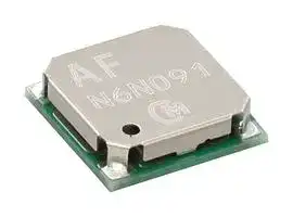
MYLSM00502ERPL
DC/DC POL Converter, Adjustable, Buck, 4.5 V to 17 V in, 1V to 5.25 V out, 2.5 A out, 2.5MHz, SMD-9
⚠️ Reference pricing provided. In case of supply shortages, we will connect you with our trusted procurement partners to ensure your project's continuity.
- Manufacturer: MURATA POWER SOLUTIONS
- Product type: DC / DC Non Isolated Board Mount Converters - Adjustable Output
- SVHC: No SVHC (04-Feb-2026)
- Depth: 7.9mm
- Width: 7.9mm
- Height: 2.3mm
- Topology: Synchronous Buck (Step Down)
- No. of Pins: 9Pins
- Product Range: MYLSM Series
- No. of Outputs: 1 Output
- Output Current: 2.5A
- Output Power Max: 13.1W
- Input Voltage Max: 17V
- Input Voltage Min: 4.5V
- Output Current Max: 2.5A
- Output Voltage Max: 5.25V
- Output Voltage Min: 1V
- Switching Frequency: 2.5MHz
- Input Voltage DC Max: 17V
- Input Voltage DC Min: 4.5V
- DC / DC Converter Type: Step Down, Module
- DC / DC Converter IC Case: SMD
- Operating Temperature Max: 85°C
- Power Supply Applications: Industrial
- DC / DC Converter Output Type: Adjustable
| Delivery and price | |
|---|---|
| Units per pack | 250 |
| Price | 3.17 € |
| Current stock | 200+ |
| Lead time | 30 days |
Datasheet

**MYLSM00502ERPL** DC-DC converter ## **Typical unit** ## **FEATURES** 4.5 - 17Vdc Input Voltage range (Absolute maximum input voltage:18Vdc) - Programmable output voltage range from 1 to 5.25Vdc Up to 2.5A of output current Ultra small surface mount package 7.9 x 7.9 x 2.3mm - High efficiency `:` 88% - Short Circuit Protection - On/Off control (Positive logic) - Operating Temperature range -40 to +85 degC ## **PRODUCT OVERVIEW** MYLSM00502EPRL is Surface Mount type of DC-DC power converter for embedded applications. The tiny form factor measures only 7.9 x 7.9 x 2.3 mm. The wide input range is 4.5 to 17Vdc. The maximum output current of 2.5A. Based on Hi-frequency synchronous buck converter switching topology, the high power conversion efficient module features programmable output voltage and On/Off control. This converter also include output short circuit protection. ## **SIMPLIFIDE APPLICATION** **==> picture [285 x 163] intentionally omitted <==** **----- Start of picture text -----**<br> MYLSM00502ERPL<br>VIN VOUT<br>RVAR<br>EN VAR<br>Vin Co<br>Cin<br>RL<br>GND GND<br>G-PAD<br>Het pi<br>Cin : 10μF/25V × 1pcs<br>Co : 47μF/6.3V × 1pcs<br>**----- End of picture text -----**<br> **http://www.murata.com/products/power** MYLSM00502ERPL A01 Page 1 of 14 **MYLSM00502ERPL** DC-DC converter |PERFORMANCESPECIFICATIONS SUMMARY ANDORDERING GUIDE|PERFORMANCESPECIFICATIONS SUMMARY ANDORDERING GUIDE|PERFORMANCESPECIFICATIONS SUMMARY ANDORDERING GUIDE|PERFORMANCESPECIFICATIONS SUMMARY ANDORDERING GUIDE|PERFORMANCESPECIFICATIONS SUMMARY ANDORDERING GUIDE|PERFORMANCESPECIFICATIONS SUMMARY ANDORDERING GUIDE|PERFORMANCESPECIFICATIONS SUMMARY ANDORDERING GUIDE|PERFORMANCESPECIFICATIONS SUMMARY ANDORDERING GUIDE|PERFORMANCESPECIFICATIONS SUMMARY ANDORDERING GUIDE|PERFORMANCESPECIFICATIONS SUMMARY ANDORDERING GUIDE|PERFORMANCESPECIFICATIONS SUMMARY ANDORDERING GUIDE|PERFORMANCESPECIFICATIONS SUMMARY ANDORDERING GUIDE|PERFORMANCESPECIFICATIONS SUMMARY ANDORDERING GUIDE| |---|---|---|---|---|---|---|---|---|---|---|---|---| |Model Number|Output||||||Input||||Efficiency<br>(%)|Package<br>(mm)| ||Vo<br>(Vdc)|Io<br>(A,Max.)|Power<br>(W)|R/N Max.<br>(mV p-p)|R/N Max.<br>Regulation||Vin typ.<br>(Vdc)|Range<br>(Vdc)|Iin, no load<br>Typ.(mA)|Iin, full load<br>Typ.(A)||| ||||||Line (%)|Load (%)||||||| |MYLSM00502EPRL|1 - 5.25|2.5|13.1|30|±2.0|±2.0|12|4.5 - 17|10|1.25|88|7.9 x 7.9 x 2.3| - 1.Specification of R/N MAX. is at typical Input voltage, Vo = 1.0V and Io = 2.5A, +25degC. Output capacitor is 47uF ceramic capacitor. Input capacitors is 10uF ceramic capacitors. See detailed specifications. Input and output capacitors are necessary for our test equipment. 2. Specification of Regulation and Efficiency are at Io = 2.5A. - 3.Use adequate ground plane and copper thickness adjacent to the converter. **==> picture [343 x 172] intentionally omitted <==** **----- Start of picture text -----**<br> PART NUMBER STRUCTURE<br>MY LSM 005 02 ERPL<br>Murata products Internal Code<br>Series Name Maximum Output Current<br>Maximum Output Voltage<br>**----- End of picture text -----**<br> ## **PRODUCT MARKING** Because of the small size of these products, the product marking contains a character-reduced code to indicate the model number and manufacturing date code. Not all items on the marking are always used. Please note that the marking differs from the product photograph. Here is the layout of the Marking. Codes **Item Contents AF** Product Code ~~a~~ `□□□□□□` Lot No. (6-digit alphanumeric) ~~a~~ M Manufacturer ID ~~CO~~ **http://www.murata.com/products/power** **==> picture [28 x 9] intentionally omitted <==** **----- Start of picture text -----**<br> Layout<br>**----- End of picture text -----**<br> **==> picture [38 x 78] intentionally omitted <==** **----- Start of picture text -----**<br> AF<br>M<br>oC<br>1pin<br>**----- End of picture text -----**<br> MYLSM00502ERPL A01 Page 2 of 14 **MYLSM00502ERPL** DC-DC converter ## **FUNCTIONAL SPECIFICATIONS** |**ABSOLUTE MAXIMUM RATINGS**|**Conditions**|**Minimum**|**Typical / Nominal**|**Maximum**|**Units**| |---|---|---|---|---|---| |**Input Voltage, Continuous**||-0.3||18|Vdc| |**EN**||-0.3||Vin|Vdc| |**VARpin**|||Source ONLY||| |**Storage Temperature Range**|Vin = Zero(nopower)|-40||85|degC| |Absolute maximums are stress ratings. Exposure of devices to greater than any of these conditions may adversely affect long-term reliability. Proper operation under conditions other<br>than those listed in the Performance/Functional Specifications Table is not implied or recommended.|||||| |**INPUT**|**Conditions**|**Minimum**|**Typical / Nominal**|**Maximum**|**Units**| |**Operating Voltage Range (Vin)**|Vin>Vo +3.0|4.5|12|17|Vdc| |**Startup threshold**|Rising input voltage<br>Vo=1V||3.6||Vdc| |**Shutdown threshold**|Shutdown input voltage<br>Vo=1V||2.9||Vdc| |**Input current**|||||| |**Full Load Conditions**|Vin = 12V,Vo = 5.25V,Io =2.5A||1.25||A| |**No Load Current**|Vin = 12V,Vo = 5.25V,Io =0A||10||mA| |**EN pin Voltage**|Power ON|1||Vin|Vdc| ||Power OFF|||0.3|Vdc| |**GENERAL**|**Conditions**|**Minimum**|**Typical / Nominal**|**Maximum**|**Units**| |**Efficiency**|Vin = 12V,Vo = 5.25V,Io = 2.5A||88||%| |**DYNAMIC CHARACTERISTICS**|**Conditions**|**Minimum**|**Typical / Nominal**|**Maximum**|**Units**| |**Fixed Switching Frequency**|Vo = 3.3V,Io = 2.5A||2500||kHz| |**Startup Time(Vin ON)**|||1.6||ms| |**Startup Time(EN ON)**|||1.6||ms| |**OUTPUT**|**Conditions**|**Minimum**|**Typical / Nominal**|**Maximum**|**Units**| |**Voltage**|||||| |**Output Voltage Range (Vo)**|RVER = 0Ω|5.09|5.25|5.41|Vdc| ||RVER = 1.047kΩ|4.85|5.0|5.15|Vdc| ||RVER = 14kΩ|3.2|3.3|3.4|Vdc| ||RVER = 96.3kkΩ|1.45|1.5|1.55|Vdc| ||RVER = 382kΩ|0.97|1.0|1.03|Vdc| |**Current**|||||| |**Output Current Range (Io)**||0||2.5|A| |**Short circuitprotection method**|Hiccupcurrent limiting||Non-latching||| |**Ripple Voltage**|Vin = 12V, Vo = 1V, Io = 2.5A<br>20 MHz BW||15|30|mV p-p| |**External Output Capacitive**|Vo≦2.5V<br>~~Po~~|47<br>~~Po~~|~~Po~~|120<br>~~Po~~|uF<br>~~Po~~| ||Vo>2.5V<br>~~Po~~<br>~~a~~|20<br>~~Po~~<br>~~QO~~|~~Po~~<br>~~QO~~|60<br>~~Po~~<br>~~QO~~|uF<br>~~Po~~<br>~~QO~~| |**MECHANICAL**|**Conditions**<br>~~a~~|**Minimum**<br>~~QO~~|**Typical / Nominal**<br>~~QO~~|**Maximum**<br>~~QO~~|**Units**<br>~~QO~~| |**Outline Dimensions**||7.9(typ.)x 7.9(typ.)x 2.3(max.)|||mm| |**Weight**|||265||mgrams| |**ENVIRONMENTAL**|**Conditions**|**Minimum**|**Typical / Nominal**|**Maximum**|**Units**| |**Operating Ambient Temperature Range**<br>~~a~~||-40||85|degC| |**Strage Temperature**<br>~~a~~||-40||85|degC| |**Moisture Sensitivity Level**||2|||| ## **SPECIFICATIONS NOTES** (1)All models are tested and specified with external 47uF ceramic output capacitors and 10uF ceramic input capacitors. All capacitors are low ESR types. These capacitors are necessary to accommodate our test equipment and may not be required to achieve specified performance in your applications. However, Murata recommends installation of these capacitors. (2)Note that Maximum Power Derating curves indicate an average current at typical input voltage. At higher temperatures and/or no airflow, the converter will tolerate brief full current outputs if the total RMS current over time does not exceed the Derating curve. (3)The On/Off Control Input should use either a switch or an open collector/open drain transistor referenced to GND. A logic gate may also be used by applying appropriate external voltages which do not exceed +Vin (4)“Hiccup” operation repeatedly attempts to restart the converter with a brief, full-current output. If the short circuit condition still exists, the restart current will be removed and then tried again. This short current pulse prevents overheating and damaging the converter. Once the fault is removed, the converter immediately recovers normal operation. (5)Do not exceed maximum power specifications when adjusting the output trim. (6)The maximum output capacitive loads depend on the Equivalent Series Resistance (ESR) of the external output capacitor and, to a lesser extent, the distance and series impedance to the load. Larger caps will reduce output noise but may change the transient response. Newer ceramic caps with very low ESR may require lower capacitor values to avoid instability. Thoroughly test your capacitors in the application. Please refer to the Output Capacitive Load Application Note. (7) Do not allow the input voltage to degrade lower than the specified minimum voltage, at all times. Otherwise, you risk having the converter turn off. The under voltage shutdown is not latching and will attempt to recover when the input is brought back into normal operating range. (8) Depending on the output condition during startup, overcurrent protection may operate. (9) When the load current decreases, the converter enters Power Save Mode. And this mode the switching frequency decreases. ## **http://www.murata.com/products/power** MYLSM00502ERPL A01 Page 3 of 14 **MYLSM00502ERPL** DC-DC converter **==> picture [239 x 7] intentionally omitted <==** **----- Start of picture text -----**<br> PERFORMANCE DATA AND OSCILLOGRAMS OF MYLSM00502EPRL<br>**----- End of picture text -----**<br> **==> picture [180 x 8] intentionally omitted <==** **----- Start of picture text -----**<br> Efficiency vs. Line Voltage and Load Current @ +25degC. (Vo = 1.0V)<br>**----- End of picture text -----**<br> **==> picture [163 x 8] intentionally omitted <==** **----- Start of picture text -----**<br> Vo vs. Line Voltage and Load Current @ +25degC. (Vo = 1.0V)<br>**----- End of picture text -----**<br> On/Off Enable Delay (Vin=12V, Vo=1.0V, Io=2.5A, Co = 47uF) Trace1=Enable, Trace2=Vo, 400us/div Output Ripple and Noise (Vin=12V, Vo=1.0V, Io=2.5A, Co = 47uF, Scope BW=20MHz) Step Load Transient Response (Vin=12V, Vo=1.0V, Co = 47uF, Io=1.25A to 2.5A, 2.5A/us) Trace 3=Vo, 20mV/div, Trace 4=Io, 2A/div. Step Load Transient Response (Vin=12V, Vo=1.0V, Co = 47uF, Io=1.25A to 2.5A, 2.5A/us) Trace 3=Vo, 20mV/div, Trace 4=Io, 2A/div. **http://www.murata.com/products/power** MYLSM00502ERPL A01 Page 4 of 14 **MYLSM00502ERPL** ## DC-DC converter **==> picture [239 x 7] intentionally omitted <==** **----- Start of picture text -----**<br> PERFORMANCE DATA AND OSCILLOGRAMS OF MYLSM00502EPRL<br>**----- End of picture text -----**<br> Efficiency vs. Line Voltage and Load Current @ +25degC. (Vo = 3.3V) Vo vs. Line Voltage and Load Current @ +25degC. (Vo = 3.3V) On/Off Enable Delay (Vin=12V, Vo=3.3V, Io=2.5A, Co = 47uF) Trace1=Enable, Trace2=Vo, 400us/div Output Ripple and Noise (Vin=12V, Vo=3.3V, Io=2.5A, Co = 47uF, Scope BW=20MHz) Step Load Transient Response (Vin=12V, Vo=3.3V, Co = 47uF, Io=1.25A to 2.5A, 2.5A/us) Trace 3=Vo, 20mV/div, Trace 4=Io, 2A/div. Step Load Transient Response (Vin=12V, Vo=3.3V, Co = 47uF, Io=1.25A to 2.5A, 2.5A/us) Trace 3=Vo, 20mV/div, Trace 4=Io, 2A/div. ## **http://www.murata.com/products/power** MYLSM00502ERPL A01 Page 5 of 14 **MYLSM00502ERPL** DC-DC converter ## PERFORMANCE DATA AND OSCILLOGRAMS OF MYLSM00502EPRL **==> picture [404 x 8] intentionally omitted <==** **----- Start of picture text -----**<br> Efficiency vs. Line Voltage and Load Current @ +25degC. (Vo = 5.25V) Vo vs. Line Voltage and Load Current @ +25degC. (Vo = 5.25V)<br>**----- End of picture text -----**<br> On/Off Enable Delay (Vin=12V, Vo=5.25V, Io=2.5A, Co = 47uF) Trace1=Enable, Trace2=Vo, 400us/div Output Ripple and Noise (Vin=12V, Vo=5.25V, Io=2.5A, Co = 47uF, Scope BW=20MHz) Step Load Transient Response (Vin=12V, Vo=5.25V, Co = 47uF, Io=1.25A to 2.5A, 2.5A/us) Trace 3=Vo, 20mV/div, Trace 4=Io, 2A/div. Step Load Transient Response (Vin=12V, Vo=5.25V, Co = 47uF, Io=1.25A to 2.5A, 2.5A/us) Trace 3=Vo, 20mV/div, Trace 4=Io, 2A/div. ## **http://www.murata.com/products/power** MYLSM00502ERPL A01 Page 6 of 14 **MYLSM00502ERPL** DC-DC converter ## **THERMAL DERATTING CURVS** ## **Maximum Current Temperature Derating at Sea Level** **==> picture [339 x 198] intentionally omitted <==** **----- Start of picture text -----**<br> Safe Operating Area<br>3.0<br>2.5<br>Pte tT tt tt<br>2.0 PAN<br>Vo5.25<br>1.5 Vo3.3<br>1.0 Vo2.5<br>N E<br>Vo1.5<br>0.5 | | ft fe | Wy) eS<br>Vo1.0<br>0.0 | | ft fF | tty<br>20 30 40 50 60 70 80 90<br>Ambient Temperature Ta [degC]<br>Output Current[A]<br>**----- End of picture text -----**<br> Thermal deratings are evaluated in following condition. ・Input Voltage is 13.2V. ・ The products are mounted on 100mm x 50mmx 1.6mm(4 Layer, 1oz copper each)FR-4 board respectively. **http://www.murata.com/products/power** eee MYLSM00502ERPL A01 Page 7 of 14 ## **MYLSM00502ERPL** muPata ~~eeseses—‘(Céi‘~CSt~~ DC-DC converter ## **MECHANICAL SPECIFICATIO** ## **Dimension and Pin Assignment** **==> picture [36 x 9] intentionally omitted <==** **----- Start of picture text -----**<br> 7.9±0.3<br>**----- End of picture text -----**<br> **==> picture [269 x 138] intentionally omitted <==** **----- Start of picture text -----**<br> AF<br>M<br>[ oooooo |<br>A loe Je<br>[Hea 【 Unit : mm 】<br>7.9±0.3<br>2.3 max.<br>**----- End of picture text -----**<br> ## <Bottom View> **==> picture [266 x 188] intentionally omitted <==** **----- Start of picture text -----**<br> 0.3 1.35 1.0 2.6 1.0 1.35 0.3<br>5 6 7<br>1<br>2-3<br>4<br>9<br>4 8 5<br>6<br>7<br>ie r al 8<br>3 2 1 9<br>1.55 1.2 0.6 1.2 0.6 1.2 1.55<br>| Tit tt<br>7.9<br>ee 【 Unit : mm 】<br>0.3<br>1.35<br>1.0 3.35<br>7.9 2.6 1.2<br>1.0<br>3.35<br>1.35<br>0.3<br>**----- End of picture text -----**<br> |**INPUT/OUTPUT CONNECTIONS**|**INPUT/OUTPUT CONNECTIONS**|**INPUT/OUTPUT CONNECTIONS**| |---|---|---| |**Pin No.**|**Name**|**Function**| |**1**|VAR|Output Voltage Adjustment| |**2-3**|GND|pgj<br>GND| |**4**|Vin|Input Voltage| |**5**|EN|Enable(ON/OFF)| |**6**|GND|GND| |**7**|Vo|Output Voltage| |**8**|GND|GND| |**9**|G-PAD|GNDpad for radiation| **http://www.murata.com/products/power** MYLSM00502ERPL A01 Page 8 of 14 **MYLSM00502ERPL** DC-DC converter ## DC-DC converter INNOVATOR IN ELECTRONICS ~~ne~~ ## **Recommended Board Land Pattern (Top View)** **==> picture [188 x 186] intentionally omitted <==** **----- Start of picture text -----**<br> 0.3 1.35 1.0 2.6 1.0 1.35 0.3<br>P 7 F P i<br>7 6 5<br>|<br>9<br>8 4<br>: Jj),Li A .<br>|<br>1 2 3<br>7<br>1.55 1.2 0.6 1.2 0.6 1.2 1.55<br>tltt<br>7.9<br>PO<br>0.3<br>1.35<br>1.0 3.35<br>7.9 2.6 1.2<br>1.0<br>3.35<br>1.35<br>0.3<br>**----- End of picture text -----**<br> ## `【` Unit `:` mm `】` ## **EXAMPLE OF PATTEAN LAYOUT (TOP VIEW)** **Picture** Top view **==> picture [178 x 219] intentionally omitted <==** **----- Start of picture text -----**<br> EN<br>Vo<br>Vin<br>rae) 0 (Co 0<br>fq<br>1pin O<br>RVAR1 RVAR2<br>GND<br>**----- End of picture text -----**<br> ## Bottom view **http://www.murata.com/products/power** MYLSM00502ERPL A01 Page 9 of 14 **MYLSM00502ERPL** DC-DC converter ## **TAPE AND REEL INFORMATION** ## **Tape Dimension** **==> picture [377 x 559] intentionally omitted <==** **----- Start of picture text -----**<br> 2.00±0.1<br>φ 1.50+0.1-0 16.00±0.1 4.00±0.1<br>B<br>att<br>Ad<br>A A ’<br>φ 1.50+0.1-0 B ’ 0.30±0.052.50±0.1<br>BEES | Section B-B “E ’ L<br>aa 8.40±0.1<br>【 Unit : mm 】<br>Section A-A ’<br>C3 lavel 21.5±1.0<br>17.5±1.0<br>|<br>A<br>IS \\<br>Susp<br>2.0±0.5<br>Individual lavel<br>φ21.0±0.8 φ13.0±0.5<br>【 Unit : mm 】<br>Portion A<br>(5°)<br>(5°)<br>1.75±0.1<br>+0.3-0.1<br>7.50±0.1<br>16.00<br>8.40±0.1<br>φ100±1 φ330±2<br>**----- End of picture text -----**<br> ## **Reel Dimension** **http://www.murata.com/products/power** MYLSM00502ERPL A01 Page 10 of 14 ## **MYLSM00502ERPL** DC-DC converter ## **TAPE SPECIFICATION** **==> picture [457 x 290] intentionally omitted <==** **----- Start of picture text -----**<br> Empty portion Empty portion Leader portion<br>C3 label (200mm MIN) (180mm MIN) (200mm MIN)<br>aN a<br>"Module on tape" portion<br>V AR )<br>Indication label<br>Circle Hole<br>cre OF<br>Oo oO O O OO OO O<br>Pull Direction<br>=<br>AF AF<br>M M<br>**----- End of picture text -----**<br> ## **Note** 1. The adhesive strength of the protective tape must be within 0.1-1.3N. - 2.Each reel contains 1000 pcs. - 3.Each reel set in moisture-proof packaging because of MSL 2. - 4.No vacant pocket in “Module on tape” section. - 5.The reel is labeled with Murata part number and quantity. - 6.The color of reel is not specified. **http://www.murata.com/products/power** MYLSM00502ERPL A01 Page 11 of 14 **MYLSM00502ERPL** DC-DC converter ## **TECHNICAL NOTES** ## **Input Fusing** Certain applications and/or safety agencies may require fuses at the inputs of power conversion components. Fuses should also be used when there is the possibility of sustained input voltage reversal which is not current limited. For greatest safety, we recommend a fast blow fuse installed in the ungrounded input supply line. The installer must observe all relevant safety standards and regulations. For safety agency approvals, install the converter in compliance with the end-user safety standard. ## **Recommended Input Filtering** The user must assure that the input source has low AC impedance to provide dynamic stability and that the input supply has little or no inductive content, including long distributed wiring to a remote power supply. For best performance, we recommend installing a low-ESR capacitor immediately adjacent to the converter’s input terminals. The capacitor should be a ceramic type such as the Murata GRM31 series or GRM21 series and a electrolytic type such as Panasonic OS-CON series. Initial suggested capacitor values are 10uF ceramic type, rated at twice the expected maximum input voltage. Make sure that the input terminals do not go below the under voltage shutdown voltage at all times. More input bulk capacitance may be added in parallel if needed. ## **Recommended Output Filtering** The converter will achieve its rated output ripple and noise with additional external capacitor. The user may install more external output capacitance reduce the ripple even further or for improved dynamic response. Initial suggested capacitor values are 47uF(Vo `≦` 2.5V) or 20uF(Vo>2.5V) ceramic type . Measure the output ripple under your load conditions. Use only as much capacitance as required to achieve your ripple and noise objectives. Excessive capacitance can make step load recovery sluggish or possibly introduce instability. Do not exceed the maximum rated output capacitance listed in the specifications. ## **Output Noise** Output noise is measured as shown in the figures below. ## **Minimum Output Loading Requirements** All models regulate within specification and are stable under no load to full load conditions. Operation under no load might however slightly increase output ripple and noise. ## **Temperature Derating Curves** The graphs in this data sheet illustrate typical operation under a variety of conditions. The derating curves show the maximum continuous ambient air temperature. Note that these are AVERAGE measurements. Note that the temperatures are of the ambient airflow, not the converter itself which is obviously running at higher temperature than the outside air. Also note that very low flow rates (below about 25 LFM) are similar to “natural convection,” that is, not using fan-forced airflow. Murata makes Characterization measurements in a closed cycle wind tunnel with calibrated airflow. We use both thermocouples and an infrared camera system to observe thermal performance. **CAUTION:** These graphs are all collected at slightly above Sea Level altitude. Be sure to reduce the derating for higher density altitude. ## **Output Short Circuit Protection** In the case of a heavy overload setting such as a short circuit, the converter temporarily stop output. Following a time-out period, the converter will restart, causing the output voltage to begin ramping up to its appropriate value. If the short-circuit condition persists, another shutdown cycle will initiate. This rapid on/off cycling is called “hiccup mode”. The hiccup cycling reduces the average output current, thereby preventing excessive internal temperatures and/or component damage. A short circuit can be tolerated indefinitely. The “hiccup” system differs from latching short circuit systems because you do not have to power down the converter to make it restart. The system will automatically restore operation as soon as the short circuit condition is removed. ## **ENABLE (On/Off) Control** The converter is enabled when EN pin voltage is 0.3V or less. Please refer to the “FUNCTIONAL SPECIFICATIONS” on page 3 for EN voltage. ## **Output Capacitive Load** Users should only consider adding capacitance to reduce switching noise and/or to handle spike current load steps. Install only enough capacitance to achieve noise objectives. Excess external capacitance may cause regulation problems, degraded transient response and possible oscillation or instability. ## **Thermal Shut down** To prevent many over temperature problems and damage, these converters include thermal shutdown circuitry. If environmental conditions cause the temperature of the DC/DC’s to rise above the Operating Temperature Range up to the shutdown temperature, an on-board electronic temperature sensor will power down the unit. When the temperature decreases below the turn-on threshold, the converter will automatically restart. **CAUTION** : If you operate too close to the thermal limits, the converter may shut down suddenly without warning. Be sure to thoroughly your application to avoid unplanned thermal shutdown. **http://www.murata.com/products/power** MYLSM00502ERPL A01 Page 12 of 14 **MYLSM00502ERPL** DC-DC converter ## **Soldering Guidelines** Murata recommends the specifications below when installing this converter. Exceeding this specifications may cause damage to the product. Your production environment may differ therefore please thoroughly review these guidelines with your process engineers. |**Reflow solder operations for surface-mountproducts**|**Reflow solder operations for surface-mountproducts**| |---|---| |**Solders**|Sn/Ag/Cu based| |**Preheat Temperature**|Less than 1degC per second| |**Reflow Zone**①|| |**Time Over Liquidus**|30 to 75 seconds| |**Temperature**|220degC and more| |**Reflow Zone**②|| |**Time Over Liquidus**|20 seconds or less| |**Temperature**|250degC and more<br>(*260degC and less)| |**Cooling Rate**|Less than 1degC per second| ## **Recommended Lead-free Solder Reflow Profile** **==> picture [195 x 148] intentionally omitted <==** **----- Start of picture text -----**<br> Reflow Zone②<br>260degC Max. 20seconds max.<br>250degC<br>220degC<br>200degC Reflow<br> Zone①<br>150degC 30 ~ seconds75<br>Preheat/Soak Zone<br>60 ~ 150seconds<br>Colling curve<br>2 ~ 3degC/seconds<br>Soldering time<br>Case surface temperature<br>**----- End of picture text -----**<br> ## **Output Voltage Adjustment** The output voltage may be adjusted over a limited range by connecting an external VAR resistor (RVAR) between the VAR pin and GND pin. The RVAR resistor must be a 1/10W precision metal film type,±0.5% accuracy or better with low temperature coefficient, ±100 ppm/degC or better. RVAR resistor value is calculated by the following equation. 80 RVAR = -18 [kΩ] Vo – 0.8 Mount the resistor close to the converter with very short leads or use a surface mount trim resistor. Do not exceed the specified limits of the output voltage or the converter’s maximum power rating when applying these resistors. Also, avoid high noise at the VAR input. However, to prevent instability, you should never connect any capacitors between VAR pin and GND pin. **CAUTION:** Do not change the RVAR while the converter is operating. ## **http://www.murata.com/products/power** MYLSM00502ERPL A01 Page 13 of 14 **MYLSM00502ERPL** DC-DC converter ## **TEST Circuit** **==> picture [334 x 101] intentionally omitted <==** **----- Start of picture text -----**<br> MYLSM00502ERPL<br>VIN VOUT A<br>RVAR<br>EN VAR Vr V<br>Vin C1 C2 C3<br>RL<br>GND GND<br>G-PAD<br>**----- End of picture text -----**<br> Vin: DC Power Supply RL: Electronic Load Device - Vr :Ripple Voltmeter RM-101(Keisokugiken) C1 :10μF/25V (GRM32DR71E106KA12 ;Murata) - C2 :47μF/6.3V (GRM31CC80J476KE18 ;Murata) - C3 :0.1μF/50V (GRM188R11H104KA93 ;Murata) **http://www.murata.com/products/power** MYLSM00502ERPL A01 Page 14 of 14
Updated at April 10, 2026
About Novapart
Novapart is a B2B electronic component broker specialising in stock shortages and cost reduction. We source hard-to-find parts and identify compliant alternatives across a catalogue of 410,000+ components from 500+ manufacturers.
Learn more →Stock Shortage Specialist
When a component is unavailable, discontinued or has an unacceptable lead time, we tap into our network of vetted European and Asian distributors to source what you need — without compromising on quality or traceability.
Request a quote →Compliant Alternatives
We identify pin-to-pin, electrically equivalent substitutes that meet the same certifications (RoHS, AEC-Q100, REACH) as your original specification — validated against datasheets, not just part numbers. Often at a lower cost.
BOM Analysis service →