
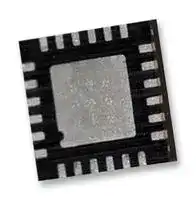


MW7IC915NT1
RF FET Transistor, 698 MHz, 960 MHz, PQFN
- Manufacturer: NXP
- Product type: RF FETs
- Drain Source Voltage Vds:-; Continuous Drain Current Id:-; Power Dissipation Pd:-; Operating Frequency Min:698MHz; Operating Frequency Max:960MHz; RF Transistor Case:PQFN; No. of Pins:24Pins;
- MSL: MSL 3 - 168 hours
- SVHC: No SVHC (27-Jun-2024)
- No. of Pins: 24Pins
- Channel Type: N Channel
- Product Range: -
- Power Dissipation: -
- Transistor Mounting: Surface Mount
- Transistor Case Style: PQFN
- Operating Frequency Max: 960MHz
- Operating Frequency Min: 698MHz
- Drain Source Voltage Vds: -
- Operating Temperature Max: 150°C
- Continuous Drain Current Id: -
| Delivery and price | |
|---|---|
| Units per pack | 50 |
| Price | 33.56 € |
| Current stock | 10+ |
| Lead time | 30 days |
**Freescale Semiconductor**
Document Number: MW7IC915N Rev. 2, 12/2013
Technical Data
## **RF LDMOS Wideband Integrated Power Amplifier**
The MW7IC915N wideband integrated circuit is designed with on--chip matching that makes it usable from 698 to 960 MHz. This multi--stage structure is rated for 26 to 32 volt operation and covers all typical cellular base station modulation formats.
## **MW7IC915NT1**
## **Driver Application — 900 MHz**
- Typical Single--Carrier W--CDMA Performance: VDD = 28 Volts, IDQ1 = 52 mA, IDQ2 = 134 mA, Pout = 1.6 Watts Avg., IQ Magnitude Clipping, Channel Bandwidth = 3.84 MHz, Input Signal PAR = 7.5 dB @ 0.01% Probability on CCDF.
||**Frequency**<br>**Gps**<br>**(dB)**<br>**PAE**<br>**(%)**<br>**ACPR**<br>**(dBc)**<br>865 MHz<br>37.9<br>17.1<br>--50.4<br>880 MHz<br>38.0<br>17.4<br>--50.6<br>895 MHz<br>37.8<br>17.5<br>--51.3<br>~~————~~|**Frequency**<br>**Gps**<br>**(dB)**<br>**PAE**<br>**(%)**<br>**ACPR**<br>**(dBc)**<br>865 MHz<br>37.9<br>17.1<br>--50.4<br>880 MHz<br>38.0<br>17.4<br>--50.6<br>895 MHz<br>37.8<br>17.5<br>--51.3<br>~~————~~|**Frequency**<br>**Gps**<br>**(dB)**<br>**PAE**<br>**(%)**<br>**ACPR**<br>**(dBc)**<br>865 MHz<br>37.9<br>17.1<br>--50.4<br>880 MHz<br>38.0<br>17.4<br>--50.6<br>895 MHz<br>37.8<br>17.5<br>--51.3<br>~~————~~||
|---|---|---|---|---|
||Capable of Handling 10:1 VSWR, @ 32 Vdc, 880 MHz, P||Capable of Handling 10:1 VSWR, @ 32 Vdc, 880 MHz, Pout= 23.5 Watts CW||
||(3 dB Input Overdrive from Rated Pout)||||
- Stable into a 5:1 VSWR. All Spurs Below --60 dBc @ 30 to 41.5 dBm CW Pout.
**728--960 MHz, 1.6 W AVG., 28 V SINGLE W--CDMA RF LDMOS WIDEBAND INTEGRATED POWER AMPLIFIER**
**PQFN 8** **8 PLASTIC**
- Typical Pout @ 1 dB Compression Point ≃ 15.5 Watts CW
## **Driver Application — 700 MHz**
- Typical Single--Carrier W--CDMA Performance: VDD = 28 Volts, IDQ1 = 50 mA, IDQ2 = 144 mA, Pout = 1.6 Watts Avg., IQ Magnitude Clipping, Channel Bandwidth = 3.84 MHz, Input Signal PAR = 7.5 dB @ 0.01% Probability on CCDF.
|**Frequency**|**Gps**<br>**(dB)**|**PAE**<br>**(%)**|**ACPR**<br>**(dBc)**|
|---|---|---|---|
|728 MHz|37.8|17.2|--49.5|
|748 MHz|37.8|17.3|--50.5|
|768 MHz|37.7|17.3|--51.4|
## **Features**
- Characterized with Series Equivalent Large--Signal Impedance Parameters and Common Source S--Parameters
- On--Chip Matching (50 Ohm Input, DC Blocked)
- Integrated Quiescent Current Temperature Compensation with Enable/Disable Function **[(1)]**
- Integrated ESD Protection
- In Tape and Reel. T1 Suffix = 1,000 Units, 16 mm Tape Width, 13--inch Reel.
> 1. Refer to AN1977, _Quiescent Current Thermal Tracking Circuit in the RF Integrated Circuit Family_ and to AN1987, _Quiescent Current Control for the RF Integrated Circuit Device Family_ . Go to http://www.freescale.com/rf. Select Documentation/Application Notes -- AN1977 orAN1987.
**MW7IC915NT1** ~~= treascaie~~
Freescale Semiconductor, Inc., 2009, 2013. All rights reserved.
**MW7IC915NT1**
RF Device Data Freescale Semiconductor, Inc.
1
**==> picture [541 x 629] intentionally omitted <==**
**----- Start of picture text -----**<br>
VGS1 VGS2<br>Quiescent Current 24 23 22 21 20 19<br>Temperature Compensation [(1)] NC 1 18 RFout/VDS2<br>GND 2 17 RFout/VDS2<br>RFin 3 16 RFout/VDS2<br>RFin 4 15 RFout/VDS2<br>RFin RFout/VDS2 GND 5 14 RFout/VDS2<br>NC 6 7 8 9 10 11 12 13 RFout/VDS2<br>VDS1<br>Figure 1. Functional Block Diagram Figure 2. Pin Connections<br>(ajo<br>1. Refer to AN1977, Quiescent Current Thermal Tracking Circuit in the RF Integrated Circuit Family and to AN1987, Quiescent Current Control<br>for the RF Integrated Circuit Device Family . Go to http://www.freescale.com/rf. Select Documentation/Application Notes -- AN1977 orAN1987.<br>Table 1. Maximum Ratings<br>Rating Symbol Value Unit<br>Drain--Source Voltage VDSS --0.5, +65 Vdc<br>Gate--Source Voltage VGS --6.0, +10 Vdc<br>Operating Voltage VDD 32, +0 Vdc<br>Storage Temperature Range Tstg --65 to +150 C<br>Operating Junction Temperature [(1)] TJ 150 C<br>Input Power Pin 17 dBm<br>Table 2. Thermal Characteristics<br>Characteristic Symbol Value [(1,2)] Unit<br>= eS<br>Thermal Resistance, Junction to Case RJC C/W<br>W--CDMA Application Stage 1, 28 Vdc, IDQ1 = 60 mA 7.5<br>(Case Temperature 82C, Pout = 1.6 W CW) Stage 2, 28 Vdc, IDQ2 = 130 mA 3.2<br>ee<br>Table 3. ESD Protection Characteristics<br>Test Methodology Class<br>Human Body Model (per JESD22--A114) 1B<br>Machine Model (per EIA/JESD22--A115) A<br>Charge Device Model (per JESD22--C101) III<br>Table 4. Moisture Sensitivity Level<br>Test Methodology Rating Package Peak Temperature Unit<br>Per JESD22--A113, IPC/JEDEC J--STD--020 3 260 C<br>——=—<br>1. MTTF calculator available at http://www.freescale.com/rf. Select Software & Tools/Development Tools/Calculators to access MTTF<br>calculators by product.<br>GS1 GS2<br>V NC V NC NC NC<br>NC DS1 DS1 NC NC NC<br>V V<br>**----- End of picture text -----**<br>
2. Refer to AN1955, _Thermal Measurement Methodology of RF Power Amplifiers._ Go to http://www.freescale.com/rf. Select Documentation/Application Notes -- AN1955.
**MW7IC915NT1**
RF Device Data Freescale Semiconductor, Inc.
2
**Table 5. Electrical Characteristics** (TA = 25C unless otherwise noted)
|**Characteristic**<br>**Symbol**<br>**Min**<br>**Typ**<br>**Max**<br>**Unit**<br>**Stage 1 — Off Characteristics**<br>Zero Gate Voltage Drain Leakage Current<br>(VDS= 65 Vdc, VGS= 0 Vdc)<br>IDSS<br>—<br>—<br>10<br>Adc<br>Zero Gate Voltage Drain Leakage Current<br>(VDS= 28 Vdc, VGS= 0 Vdc)<br>IDSS<br>—<br>—<br>1<br>Adc<br>Gate--Source Leakage Current<br>(VGS= 1.5 Vdc, VDS= 0 Vdc)<br>IGSS<br>—<br>—<br>1<br>Adc<br>**Stage 1 — On Characteristics**<br>Gate Threshold Voltage<br>(VDS= 10 Vdc, ID= 9Adc)<br>VGS(th)<br>1<br>2<br>3<br>Vdc<br>Gate Quiescent Voltage<br>(VDS= 28 Vdc, ID= 52 mAdc)<br>VGS(Q)<br>—<br>3<br>—<br>Vdc<br>Fixture Gate Quiescent Voltage<br>(VDD= 28 Vdc, ID= 52 mAdc, Measured in Functional Test)<br>VGG(Q)<br>5.5<br>6.3<br>7<br>Vdc<br>**Stage 2 — Off Characteristics**<br>Zero Gate Voltage Drain Leakage Current<br>(VDS= 65 Vdc, VGS= 0 Vdc)<br>IDSS<br>—<br>—<br>10<br>Adc<br>Zero Gate Voltage Drain Leakage Current<br>(VDS= 28 Vdc, VGS= 0 Vdc)<br>IDSS<br>—<br>—<br>1<br>Adc<br>Gate--Source Leakage Current<br>(VGS= 1.5 Vdc, VDS= 0 Vdc)<br>IGSS<br>—<br>—<br>1<br>Adc<br>~~— EE~~<br>~~—~~<br>~~EE~~<br>~~——~~|
|---|
|**Stage 2 — On Characteristics**|
|Gate Threshold Voltage<br>(VDS= 10 Vdc, ID= 36Adc)<br>VGS(th)<br>1<br>2<br>3<br>Vdc<br>Gate Quiescent Voltage<br>(VDS= 28 Vdc, ID= 134 mAdc)<br>VGS(Q)<br>—<br>2.9<br>—<br>Vdc<br>Fixture Gate Quiescent Voltage<br>(VDD= 28 Vdc, ID= 134 mAdc, Measured in Functional Test)<br>VGG(Q)<br>3.8<br>4.6<br>5.3<br>Vdc<br>Drain--Source On--Voltage<br>(VGS= 10 Vdc, ID= 3.6 Adc)<br>VDS(on)<br>0.1<br>0.3<br>0.8<br>Vdc<br>~~EEE~~|
|**Functional Tests (1)** (In Freescale Test Fixture, 50 ohm system) VDD= 28 Vdc, IDQ1= 52 mA, IDQ2= 134 mA, Pout= 1.6 W Avg.,|
|f = 880 MHz, Single--Carrier W--CDMA, IQ Magnitude Clipping, Input Signal PAR = 7.5 dB @ 0.01% Probability on CCDF. ACPR measured|
|in 3.84 MHz Channel Bandwidth @5 MHz Offset.|
|Power Gain<br>Gps<br>35.0<br>38.0<br>41.0<br>dB<br>Power Added Efficiency<br>PAE<br>15.0<br>17.4<br>—<br>%<br>Adjacent Channel Power Ratio<br>ACPR<br>—<br>--50.6<br>--47.0<br>dBc<br>Input Return Loss<br>IRL<br>—<br>--22<br>--9<br>dB<br>~~SS~~|
|**Typical Performance over Frequency**(In Freescale Test Fixture, 50 ohm system) VDD= 28 Vdc, IDQ1= 52 mA, IDQ2= 134 mA, Pout= 1.6 W|
|Avg., Single--Carrier W--CDMA, IQ Magnitude Clipping, Input Signal PAR = 7.5 dB @ 0.01% Probability on CCDF. ACPR measured in|
|3.84 MHz Channel Bandwidth @5 MHz Offset.|
|**Frequency**<br>**Gps**<br>**(dB)**<br>**PAE**<br>**(%)**<br>**ACPR**<br>**(dBc)**<br>**IRL**<br>**(dB)**<br>865 MHz<br>37.9<br>17.1<br>--50.4<br>--21<br>880 MHz<br>38.0<br>17.4<br>--50.6<br>--22<br>895 MHz<br>37.8<br>17.5<br>--51.3<br>--22<br>~~tee~~|
|1. Part internally input matched.|
(continued)
**MW7IC915NT1**
RF Device Data Freescale Semiconductor, Inc.
3
**Table 5. Electrical Characteristics** (TA = 25C unless otherwise noted) **(continued)**
|**Typical Performances**(In Freescale Test Fixture, 50 ohm system) VDD= 28 Vdc, I|= 28 Vdc, IDQ1= 52 mA, I|= 52 mA, IDQ2= 134 mA, 865--895 MHz Bandwidth|= 134 mA, 865--895 MHz Bandwidth|= 134 mA, 865--895 MHz Bandwidth|= 134 mA, 865--895 MHz Bandwidth|
|---|---|---|---|---|---|
|Pout@ 1 dB Compression Point, CW<br>(VDD= 28 Vdc, IDQ1= 75 mA, IDQ2= 100 mA)|P1dB|—|15.5|—|W|
|IMD Symmetry @ 16 W PEP, Poutwhere IMD Third Order<br>Intermodulation30 dBc<br>(Delta IMD Third Order Intermodulation between Upper and Lower<br>Sidebands > 2 dB)|IMDsym|—|45|—|MHz|
|VBW Resonance Point<br>(IMD Third Order Intermodulation Inflection Point)|VBWres|—|180|—|MHz|
|Quiescent Current Accuracy over Temperature **(1)**<br>Stage 1<br>with 2 kGate Feed Resistors (--30 to 85C)<br>Stage 2|IQT|—<br>—|0.10<br>0.12|—<br>—|%|
|Gain Flatness in 30 MHz Bandwidth @ Pout= 1.6 W Avg.|GF|—|0.1|—|dB|
|Gain Variation over Temperature<br>(--30C to +85C)|G|—|0.041|—|dB/C|
|Output Power Variation over Temperature<br>(--30C to +85C)|P1dB|—|0.004|—|dBm/C|
|3.84 MHz Channel Bandwidth @5 MHz Offset.|||||
|---|---|---|---|---|
|**Frequency**|**Gps**<br>**(dB)**|**PAE**<br>**(%)**|**ACPR**<br>**(dBc)**|**IRL**<br>**(dB)**|
|728 MHz|37.8|17.2|--49.5|--23|
|748 MHz|37.8|17.3|--50.5|--22|
|768 MHz|37.7|17.3|--51.4|--22|
1. Refer to AN1977, _Quiescent Current Thermal Tracking Circuit in the RF Integrated Circuit Family_ and to AN1987, _Quiescent Current Control for the RF Integrated Circuit Device Family_ . Go to http://www.freescale.com/rf. Select Documentation/Application Notes -- AN1977 or AN1987.
**MW7IC915NT1**
RF Device Data Freescale Semiconductor, Inc.
4
**==> picture [493 x 258] intentionally omitted <==**
**----- Start of picture text -----**<br>
° ° °° 5 °° VG1 VG2 C8 C10 [C12] C19 N 0900000=>»<br>) 0 R1 = fa R2 N<br>°° 50 OO] [| ° || STO/o0 0/0 0p 0000000070000 ) 00000000000° °00000000000000000000<br>° oO o| (Lm o 8<br>° ° Piri ane) S — | N<br>6° °3 6 09 000001 000 |}| 0|0000000000000000 ol° loo 00 2oS8 iS_ ]G 00000000 bo0000 SS<br>3 ° c f . bg 0 8 ° C13 C15 = °<br>° ° =e 5 lo fe) ooo) ° C17 °<br>° } f_\__\ lo 9 ° ° VD2<br>° ODDDDA/GDGD\CDOADDDDDO0D0000GC00000G ol lo ro ° °<br>°° C7 C9 C11 3 lolo feoo000000000° °°<br>° fe) Oo lio °<br>° oO ol lo °<br>°} Po oosfoKeYe) iS A ooCC OOO°<br>° JO S Olo °<br>° d lo °<br>oocoo000000000000000000DNO0NDNDNODNODNONONONONO000N0N0N0 OP OUO00 pPeooooooooeooOoOoOoOoOoOoOoOoOoOOoOCOoOOOoOoOOOoOoOOO00O0ON0<br>d000°0° C1 DOOCDDCDDDDDCDDDDD0D0000000000—%e. C2 °Eile) omooo aeoO° POSS TT C3 D O C4 — THSOOO OOOO TT OE C5 TOOOGO C6 O/OOO0°°°<br>° ot JOO 000 ooo0°0 ooo0000<br>° 2so" fi freescall e v fe)q } C14 °8<br>° semiconductor ° °<br>° i) ° o2e2oc0c o p a 00 °<br>° MW7IC915N a//b T s °<br>6 ° Rev 3 ° $ ° ima C16 C18 8 VD1<br>° ° ° ° [oxexe) °<br>° ° ° ° o 2 ° — °<br>° ° ge 90000 o 6 O©000000000 ooo0g<br>°° °° 22oo00 —|/<br>° ° ©6<br>° 9 ©0000000000 000000000000000000000<br>C20<br>**----- End of picture text -----**<br>
**Figure 3. MW7IC915NT1 Test Circuit Component Layout**
**Table 6. MW7IC915NT1 Test Circuit Component Designations and Values**
|**Part**|**Description**|**Part Number**|**Manufacturer**|
|---|---|---|---|
|C1|1.8 pF Chip Capacitor|ATC100B1R8BT500XT|ATC|
|C2, C5|0.8 pF Chip Capacitors|ATC100B0R8BT500XT|ATC|
|C3|6.2 pF Chip Capacitor|ATC100B6R2BT500XT|ATC|
|C4|3.3 pF Chip Capacitor|ATC100B3R3CT500XT|ATC|
|C6, C11, C12, C13, C14|47 pF Chip Capacitors|ATC100B470JT500XT|ATC|
|C7, C8|1F Chip Capacitors|GRM31MR71H105KA88L|Murata|
|C9, C10|0.1F Chip Capacitors|GRM32MR71H104JA01L|Murata|
|C15, C16|4.7F Chip Capacitors|GRM31CR71H475KA12L|Murata|
|C17, C18|10F, 50 V Chip Capacitors|GRM55DR61H106KA88L|Murata|
|C19, C20|100F, 50 V Electrolytic Capacitors|MCGPR50V107M8X11--RH|Multicomp|
|R1, R2|2 k, 1/4 W Resistors|CRCW12062K00FKEA|Vishay|
|PCB|0.020,r = 3.66|RO4350B|Rogers|
**MW7IC915NT1**
RF Device Data Freescale Semiconductor, Inc.
5
## **TYPICAL CHARACTERISTICS**
**==> picture [345 x 179] intentionally omitted <==**
**----- Start of picture text -----**<br>
40 19<br>PAE<br>39 18<br>aae>>——<2<br>Gps<br>38 17<br>aes<br>37 VDD = 28 Vdc, Pout = 1.6 W (Avg.), IDQ1 = 52 mA CTI 16<br>IDQ2 = 134 mA, Single--Carrier W--CDMA, 3.84 MHz<br>36 Channel Bandwidth, Input Signal PAR = 7.5 dB @ SI --46<br>35 0.01% Probability on CCDF IRL --47 --10 0.5<br>TN<br>34 --48 --20 0<br>SS<br>33 PARC --49 --30 --0.5<br>ACPR<br>32 P pSERASS --50 --40 --1<br>800 820 840 860 880 900 920 940 960 980 1000<br>f, FREQUENCY (MHz)<br>EFFICIENCY (%)<br>PAE, POWER ADDED<br>, POWER GAIN (dB)<br>ps<br>G<br>ACPR (dBc)<br>PARC (dB)<br>IRL, INPUT RETURN LOSS (dB)<br>**----- End of picture text -----**<br>
**Figure 4. Output Peak--to--Average Ratio Compression (PARC) Broadband Performance @ Pout = 1.6 Watts Avg.**
**==> picture [356 x 390] intentionally omitted <==**
**----- Start of picture text -----**<br>
--5<br>--10 V DD = 28 Vdc, P out = 16 W (PEP), I DQ1 = 52 mA PTE<br>--15 I DQ2 = 134 mA, Two--Tone Measurements PLT,<br>--20 (f1 + f2)/2 = Center Frequency of 880 MHz<br>--25 IM3--U ||<br>--30 a a|<br>IM3--L<br>--35<br>IM5--U<br>--40 SSee eee<br>--45 ee IM5--L ae<br>--50 ee IM7--U ctl ee<br>--55 a eS) IM7--L<br>--60 PENI<br>--65 rT eT ETENT<br>--70 a eeeee<br>1 10 100 200<br>TWO--TONE SPACING (MHz)<br>Figure 5. Intermodulation Distortion Products<br>versus Two--Tone Spacing<br>40 1 60 --20<br>VDD = 28 Vdc, IDQ1 = 52 mA, IDQ2 = 134 mA, f = 880 MHz<br>Single--Carrier W--CDMA, 3.84 MHz Channel Bandwidth<br>39.5 0 PARC ~S --1 dB = 3.8 W —— 50 --25<br>39 --1 40 --30<br>P Gps N) er<br>--2 dB = 5.2 W<br>38.5 --2 30 --35<br>— ee --3 dB = 6.9 W<br>PAE<br>38 --3 20 --40<br>rN<br>37.5 --4 ACPR Input Signal PAR = 7.5 dB @ 0.01% 10 --45<br>Probability on CCDF<br>37 --5 A] S$ 0 --50<br>2 4 6 8 10<br>Pout, OUTPUT POWER (WATTS)<br>IMD, INTERMODULATION DISTORTION (dBc)<br>ACPR (dBc)<br>, POWER GAIN (dB)<br>ps<br>G<br>PROBABILITY ON CCDF (dB)<br>OUTPUT COMPRESSION AT 0.01% PAE, POWER ADDED EFFICIENCY (%)<br>**----- End of picture text -----**<br>
**Figure 6. Output Peak--to--Average Ratio Compression (PARC) versus Output Power**
**MW7IC915NT1**
RF Device Data Freescale Semiconductor, Inc.
6
## **TYPICAL CHARACTERISTICS**
**==> picture [303 x 390] intentionally omitted <==**
**----- Start of picture text -----**<br>
41 90 --15<br>VDD = 28 Vdc, IDQ1 = 52 mA, IDQ2 = 134 mA, Single--Carrier<br>40 W--CDMA, 3.84 MHz Channel Bandwidth, Input Signal 80 --20<br>PAR = 7.5 dB @ 0.01% Probability on CCDF<br>39 70 --25<br>895 MHz<br>38 Gps 60 --30<br>895 MHz 880 MHz 865 MHz<br>37 50 --35<br>880 MHz<br>36 880 MHz 40 --40<br>895 MHz 865 MHz<br>35 30 --45<br>ACPR<br>34 Ay 20 --50<br>33 L PAE T 10 --55<br>1 10 20<br>Pout, OUTPUT POWER (WATTS) AVG.<br>Figure 7. Single--Carrier W--CDMA Power Gain, Power Added<br>Efficiency and ACPR versus Output Power<br>40 0<br>Gain<br>30 --5<br>Noa<br>20 i <a --10<br>10 --15<br>fi Np<br>0 Pi VDD = 28 Vdc of --20<br>Pin = --30 dBm i\f\p IRL<br>--10 I DQ1 = 52 mA --25<br>IDQ2 = 134 mA Vy<br>--20 ‘tT --30<br>| ft<br>300 600 900 1200<br>f, FREQUENCY (MHz)<br>, POWER GAIN (dB) ACPR (dBc)<br>ps<br>G<br>PAE, POWER ADDED EFFICIENCY (%)<br>GAIN (dB) IRL (dB)<br>**----- End of picture text -----**<br>
**Figure 8. Broadband Frequency Response**
## **W--CDMA TEST SIGNAL**
**==> picture [500 x 205] intentionally omitted <==**
**----- Start of picture text -----**<br>
100 =a 10 CCC<br>0<br>10<br>--10<br>pol | | | es ee<br>3.84 MHz<br>1 --20 Channel BW<br>F EC Input Signal ES --30 EEE A=<br>0.1<br>--40<br>ptt tO NEE eee SEE<br>0.01 --50<br>W--CDMA. ACPR Measured in 3.84 MHz --60 --ACPR in 3.84 MHz +ACPR in 3.84 MHz<br>0.00010.001 poNE Channel Bandwidth @Input Signal PAR = 7.5 dB @ 0.01%Probability on CCDF 5 MHz Offset. Ne . --70--80 CEPAeeGee Integrated BW ee Integrated BW<br>0 1 2 3 4 5 6 7 8 9 10 --90 =ee<br>PEAK--TO--AVERAGE (dB) --100 SEC<br>e ere<br>Figure 9. CCDF W--CDMA IQ Magnitude --9 --7.2 --5.4 --3.6 --1.8 0 1.8 3.6 5.4 7.2 9<br>Clipping, Single--Carrier Test Signal<br>f, FREQUENCY (MHz)<br>(dB)<br>PROBABILITY (%)<br>**----- End of picture text -----**<br>
**Figure 10. Single--Carrier W--CDMA Spectrum**
**MW7IC915NT1**
RF Device Data Freescale Semiconductor, Inc.
7
VDD = 28 Vdc, IDQ1 = 52 mA, IDQ2 = 134 mA, Pout = 1.6 W Avg.
||**f**|||**Zin**|||**Zload**||
|---|---|---|---|---|---|---|---|---|
||**MHz**||||||||
||820|||52.99 -- j29.47|||7.72 + j13.96||
||840|||49.35 -- j27.56|||7.34 + j14.74||
||860|||46.67 -- j23.60|||7.43 + j15.55||
||880|||44.88 -- j17.63|||7.94 + j16.07||
||900|||43.73 -- j10.46|||7.98 + j16.74||
||920|||43.12 -- j2.75|||7.80 + j17.62||
||940|||43.38 + j5.01|||8.28 + j18.33||
||960|||44.07 + j12.97|||9.07 + j19.04||
||980|||43.89 + j12.61|||9.14 + j20.02||
|Zin<br>=|||Device input impedance as measured from||||||
||||gate to ground.||||||
|Zload<br>=|||Test circuit impedance as measured from|||Test circuit impedance as measured from|||
||||drain to ground.||||||
|||Device<br>Under Test<br>Output<br>Matching<br>Network<br>~~v~~a=|||||||
|||**Zin**||**Zload**|||||
**Figure 11. Series Equivalent Input and Load Impedance**
**MW7IC915NT1**
RF Device Data Freescale Semiconductor, Inc.
8
## **ALTERNATIVE PEAK TUNE LOAD PULL CHARACTERISTICS**
VDD = 28 Vdc, IDQ1 = 52 mA, IDQ2 = 134 mA, Pulsed CW, 10 sec(on), 10% Duty Cycle
**==> picture [234 x 175] intentionally omitted <==**
**----- Start of picture text -----**<br>
48<br>47<br>46 aa T f = 865 MHz Te van Ideal<br>45 f = 895 MHz<br>44 P r a Actual<br>43 aa ee arsine<br>42 f = 895 MHz<br>41 Se < A f = 865 MHz<br>40 rT f = 880 MHz f = 880 MHz<br>39 aa a _<br>38 a<br>37 PAPE<br>AEE<br>36 EE EEE ee r<br>0 2 4 6 8 10 12<br>Pin, INPUT POWER (dBm)<br>, OUTPUT POWER (dBm)<br>out<br>P<br>**----- End of picture text -----**<br>
NOTE: Load Pull Test Fixture Tuned for Peak P1dB Output Power @ 28 V
|**f**<br>**(MHz)**|**P1dB**|**P1dB**|**P3dB**|**P3dB**|
|---|---|---|---|---|
||**Watts**|**dBm**|**Watts**|**dBm**|
|865|18.1|42.6|22.4|43.5|
|880|18.5|42.7|22.3|43.5|
|895|18.5|42.7|22.2|43.5|
Test Impedances per Compression Level
|**f**<br>**(MHz)**||**Zsource**<br>|**Zload**<br>|
|---|---|---|---|
|865|P1dB|48.7 + j15.6|6.8 + j6.5|
|880|P1dB|52.3 + j20.8|6.9 + j6.7|
|895|P1dB|55.1 + j22.2|7.4 + j6.7|
**Figure 12. Pulsed CW Output Power versus Input Power @ 28 V**
**MW7IC915NT1**
RF Device Data Freescale Semiconductor, Inc.
9
**==> picture [505 x 488] intentionally omitted <==**
**----- Start of picture text -----**<br>
|||||||||||||||||||||
|---|---|---|---|---|---|---|---|---|---|---|---|---|---|---|---|---|---|---|---|
|O°°|°5|°|VG1|VG2|C9|000000oN|
|°°°|°O|R1|M5|_||[|me|R2|c0000/00000000000T00000|00000000000|o0000000T00000000000|C16|
|°|oo0]°|&|||°o}||[kW—|,|fo}|oo80|
|°|°|°|—|_|ar°|
|°|3|©|000002|0000000000000000000000|ol|loo|od|8s|lO00000000000|000|
|°|°|||||lo|co|eas)|lo|—|°|
|°|°|SS|°|lo|oO}|foKone)|lo|C14|°|
|°°|ge00000000/000090000900000000000|0|Od|ol|{e)BOfe)|—|Iowt|C12|°fe)|VD2|
|°°°|C8|fo)9|fo)ol|lolooO|00000|C10|&S|0|000|°°°|
|°|9|om omomomonte)|
|°|booo|°|
|°|JO|2|Olo|°|
|°|d|lo|°|
|©|CXOXDDDD20000000000000000000000000000|04|OUG00|lW®9XPXDXDX00D000000000000000000000000000000|
|006°|C1|dO000|C2|~|THTO000000000000000000000|C3|—°|omooo|poo|OCT|C4|TOOT|OO|C5|ETOOOOOO OO OOO O|OO|S|C6|OOOHOOO°|
|°°|oO|on|C7|°|
|°|egeo|fP|eces|000|o|(+)|ooegooe|
|°°}°|CG|)oe#&|freescalesem|i|conductorle|J}9fe)|||°|e°|of9ec0|00|C11|Ano|OO|rs2°|
|6°°|MW7IC915NRev 3|°°|°°°|°S°|O000-6|ima°|C13|C15|°$°|VD1|
|°|fo}|°|O°|°|_———|||fo}|
|8|°|geo|90000|2|6°|Q0002000000|Qo009|
|°|3|2|0||/|
|°|°|ae)2|6|—|
|°|°|oo|
|°|9|00000000000|000000000000000000000|
|5}|C17|°5|000000|
|°|°|
|20000000900000000000000000000000|D90000000000000000000000000000000000000000000000000000|
|Figure 13. MW7IC915NT1 Test Circuit Component Layout — 700 MHz|
|Table 7. MW7IC915NT1 Test Circuit Component Designations and Values — 700 MHzponent Designations and Values — 700 MHzonent Designations and Values — 700 MHzgnations and Values — 700 MHznations and Values — 700 MHz|
|Part|Description|Part Number|Manufacturer|
|C1, C3, C6|2.7 pF Chip Capacitors|ATC100B2R7BT500XT|ATC|
|C2|0.3 pF Chip Capacitor|ATC100B0R3BT500XT|ATC|
|C4|4.7 pF Chip Capacitor|ATC100B4R7CT500XT|ATC|
|C5|5.6 pF Chip Capacitor|ATC100B5R6CT500XT|ATC|
|C7, C8, C9, C10, C11|47 pF Chip Capacitors|ATC100B470JT500XT|ATC|
|C12, C13|4.7 F Chip Capacitors|GRM31CR71H475KA12L|Murata|
|C14, C15|10 F, 50 V Chip Capacitors|GRM55DR61H106KA88L|Murata|
|C16, C17|100 F, 50 V Electrolytic Capacitors|MCGPR50V107M8X11--RH|Multicomp|
|R1, R2|2 k, 1/4 W Resistors|CRCW12062K00FKEA|Vishay|
|PCB|0.020, r|= 3.66|RO4350B|Rogers|
**----- End of picture text -----**<br>
**Table 7. MW7IC915NT1 Test Circuit Component Designations and Values — 700 MHzponent Designations and Values — 700 MHzonent Designations and Values — 700 MHzgnations and Values — 700 MHznations and Values — 700 MHz**
**MW7IC915NT1**
RF Device Data Freescale Semiconductor, Inc.
10
**TYPICAL CHARACTERISTICS — 700 MHz**
**==> picture [353 x 604] intentionally omitted <==**
**----- Start of picture text -----**<br>
38.8 17.5<br>PAE<br>38.6 17<br>pf | ft | ft |<br>38.4 Tel | | | 7 16.5<br>VDD = 28 Vdc<br>38.2 Pout = 1.6 W (Avg.), IDQ1 = 50 mA N11 16<br>38 IChannel BandwidthDQ2 = 144 mA, Single--Carrier W--CDMA, 3.84 MHz, Input Signal PAR = 7.5 dB @ Gps --49<br>0.01% Probability on CCDF --10 0.5<br>PARC<br>37.8 --50<br>--20 0<br>IRL<br>37.6 pePo PSST [EE] | --51 --30 --0.5<br>ACPR<br>37.4 Pt | | | |Tey --52 --40 --1<br>710 720 730 740 750 760 770 780 790<br>f, FREQUENCY (MHz)<br>Figure 14. Output Peak--to--Average Ratio Compression (PARC)<br>Broadband Performance @ Pout = 1.6 Watts Avg.out = 1.6 Watts Avg. = 1.6 Watts Avg.<br>41 90 --15<br>VDD = 28 Vdc, IDQ1 = 50 mA, IDQ2 = 144 mA, Single--Carrier<br>40 W--CDMA, 3.84 MHz Channel Bandwidth, Input Signal 80 --20<br>PAR = 7.5 dB @ 0.01% Probability on CCDF<br>39 70 --25<br>38 4 728 MHz 60 --30<br>Gps 728 MHz<br>37 768 MHz 748 MHz 50 --35<br>748 MHz<br>36 748 MHz YYAY 40 --40<br>35 768 MHz L T PAE 768 MHz _ | 30 --45<br>ACPR<br>34 FA 20 --50<br>33 i | |i iii 10 --55<br>1 10 20<br>Pout, OUTPUT POWER (WATTS) AVG.<br>Figure 15. Single--Carrier W--CDMA Power Gain, Power Added<br>Efficiency and ACPR versus Output Power<br>40 0<br>Gain<br>30 Ue --10<br>20 Nf --20<br>PA<br>10 iV --30<br>fi IN<br>VDD = 28 Vdc<br>IRL<br>Pin = --30 dBm<br>0 --40<br>IDQ1 = 50 mA<br>IDQ2 = 144 mA<br>--10 poi --50<br>300 600 900 1200<br>f, FREQUENCY (MHz)<br>EFFICIENCY (%)<br>PAE, POWER ADDED<br>, POWER GAIN (dB)<br>ps<br>G<br>ACPR (dBc)<br>PARC (dB)<br>IRL, INPUT RETURN LOSS (dB)<br>, POWER GAIN (dB) ACPR (dBc)<br>ps<br>G<br>PAE, POWER ADDED EFFICIENCY (%)<br>GAIN (dB) IRL (dB)<br>**----- End of picture text -----**<br>
**Figure 14. Output Peak--to--Average Ratio Compression (PARC) Broadband Performance @ Pout = 1.6 Watts Avg.out = 1.6 Watts Avg. = 1.6 Watts Avg.**
**Figure 16. Broadband Frequency Response**
**MW7IC915NT1**
RF Device Data Freescale Semiconductor, Inc.
11
VDD = 28 Vdc, IDQ1 = 50 mA, IDQ2 = 144 mA, Pout = 1.6 W Avg.
||**f**|||**Zin**|||**Zload**||
|---|---|---|---|---|---|---|---|---|
||**MHz**||||||||
||710|||54.61 -- j2.01|||9.57 + j6.52||
||720|||55.46 + j0.26|||9.95 + j7.04||
||730|||56.75 + j2.12|||10.70 + j7.79||
||740|||58.35 + j3.55|||11.39 + j8.18||
||750|||60.11 + j4.65|||11.41 + j8.07||
||760|||61.83 + j5.22|||11.00 + j7.90||
||770|||63.19 + j5.31|||10.88 + j7.88||
||780|||64.01 + j4.90|||11.41 + j7.87||
||790|||64.18 + j3.91|||12.32 + j7.61||
|Zin<br>=|||Device input impedance as measured from||||||
||||gate to ground.||||||
|Zload<br>=|||Test circuit impedance as measured from|||Test circuit impedance as measured from|||
||||drain to ground.||||||
|||Device<br>Under Test<br>Output<br>Matching<br>Network<br>~~v~~a=|||||||
|||**Zin**||**Zload**|||||
**Figure 17. Series Equivalent Input and Load Impedance — 700 MHz**
**MW7IC915NT1**
RF Device Data Freescale Semiconductor, Inc.
12
## **PACKAGE DIMENSIONS**
**MW7IC915NT1**
RF Device Data Freescale Semiconductor, Inc.
13
**MW7IC915NT1**
RF Device Data Freescale Semiconductor, Inc.
14
**MW7IC915NT1**
RF Device Data Freescale Semiconductor, Inc.
15
## **PRODUCT DOCUMENTATION, TOOLS AND SOFTWARE**
Refer to the following documents to aid your design process.
## **Application Notes**
- AN1955: Thermal Measurement Methodology of RF Power Amplifiers
- AN1977: Quiescent Current Thermal Tracking Circuit in the RF Integrated Circuit Family
- AN1987: Quiescent Current Control for the RF Integrated Circuit Device Family
- **Engineering Bulletins**
- EB212: Using Data Sheet Impedances for RF LDMOS Devices
## **Software**
- Electromigration MTTF Calculator
- RF High Power Model
- .s2p File
For Software and Tools, do a Part Number search at http://www.freescale.com, and select the “Part Number” link. Go to the Software & Tools tab on the part’s Product Summary page to download the respective tool.
## **REVISION HISTORY**
The following table summarizes revisions to this document.
|**Revision**|**Date**|**Description**|
|---|---|---|
|0|Sept. 2009|<br>Initial Release of Data Sheet|
|1|Dec. 2009|<br>Table 4, Moisture Sensitivity Level, corrected Package Peak Temperature to 260C, p. 2|
|2|Dec. 2013|<br>Table 1, Maximum Ratings: increased input power from 4.7 dBm to 17 dBm to reflect the true capability of<br>the device, p. 2<br><br>Table 3, ESD Protection Characteristics, removed the word “Minimum” after the ESD class rating. ESD<br>ratings are characterized during new product development but are not 100% tested during production. ESD<br>ratings provided in the data sheet are intended to be used as a guideline when handling ESD sensitive<br>devices, p. 2<br><br>Table 6, Test Circuit Component Designations and Values: corrected C9, C10 chip capacitor description<br>from 0.01 to 0.1 pF, p. 5. Table 6 (900 MHz component designations) and Table 7 (700 MHz component<br>designations): added PCB material information, pp. 5, 10<br><br>Replaced Case Outline 98ASA10760D, Rev. O with Rev. A, pp. 13--15. Mechanical outline drawing<br>modified to reflect the correct lead end features. Format of the mechanical outline was also updated to the<br>current Freescale format for Freescale mechanical outlines.|
**MW7IC915NT1**
RF Device Data Freescale Semiconductor, Inc.
16
## _**How to Reach Us:**_
**Home Page:** freescale.com
**Web Support:** freescale.com/support
Information in this document is provided solely to enable system and software implementers to use Freescale products. There are no express or implied copyright licenses granted hereunder to design or fabricate any integrated circuits based on the information in this document.
Freescale reserves the right to make changes without further notice to any products herein. Freescale makes no warranty, representation, or guarantee regarding the suitability of its products for any particular purpose, nor does Freescale assume any liability arising out of the application or use of any product or circuit, and specifically disclaims any and all liability, including without limitation consequential or incidental damages. “Typical” parameters that may be provided in Freescale data sheets and/or specifications can and do vary in different applications, and actual performance may vary over time. All operating parameters, including “typicals,” must be validated for each customer application by customer’s technical experts. Freescale does not convey any license under its patent rights nor the rights of others. Freescale sells products pursuant to standard terms and conditions of sale, which can be found at the following address: freescale.com/SalesTermsandConditions.
Freescale and the Freescale logo are trademarks of Freescale Semiconductor, Inc., Reg. U.S. Pat. & Tm. Off. All other product or service names are the property of their respective owners.
E 2009, 2013 Freescale Semiconductor, Inc.
**MW7IC915NT1** & freescale
**MW7IC915NT1**
Document Number: MW7IC915NRF Device Data Rev. 2, 12/2013Freescale Semiconductor, Inc.
17
Updated at April 10, 2026
NXP Semiconductors is a global leader in secure connectivity solutions, driving innovation across the automotive, industrial, IoT, mobile, and communications infrastructure markets. By developing advanced, purpose-built technologies, NXP enables devices to sense, think, connect, and act intelligently, delivering rigorously tested components that make the connected world safer and more efficient. Within the semiconductor space, NXP is highly regarded for its extensive range of high-performance integrated circuits and discrete devices. The brand's portfolio excels in drivers and interfaces, featuring a comprehensive selection of I/O expanders designed to streamline complex system architectures. For demanding high-frequency and wireless applications, NXP provides industry-leading RF FETs and RF/PIN diodes engineered to deliver exceptional signal integrity, efficiency, and reliability. The NXP product lineup further extends to essential discrete components, including versatile bipolar transistors, JFETs, and small signal diodes optimized for precision switching and amplification. Additionally, the portfolio supports advanced automation and smart applications with precision IC sensors, such as MEMS accelerometers, alongside specialized power management solutions like AC/DC LED driver ICs and single MOSFETs for cutting-edge electronics design.
About Novapart
Novapart is a B2B electronic component broker specialising in stock shortages and cost reduction. We source hard-to-find parts and identify compliant alternatives across a catalogue of 410,000+ components from 500+ manufacturers.
Learn more →Stock Shortage Specialist
When a component is unavailable, discontinued or has an unacceptable lead time, we tap into our network of vetted European and Asian distributors to source what you need — without compromising on quality or traceability.
Request a quote →Compliant Alternatives
We identify pin-to-pin, electrically equivalent substitutes that meet the same certifications (RoHS, AEC-Q100, REACH) as your original specification — validated against datasheets, not just part numbers. Often at a lower cost.
BOM Analysis service →