


MUR480ERLG
Standard Recovery Diode, 800 V, 4 A, Single, 1.85 V, 75 ns, 70 A
- Manufacturer: ONSEMI
- Product type: Standard Recovery Rectifier Diodes
- Repetitive Reverse Voltage Vrrm Max:800V; Forward Current If(AV):4A; Diode Configuration:Single; Forward Voltage VF Max:1.85V; Reverse Recovery Time trr Max:75ns; Forward Surge Curr
- SVHC: No SVHC (25-Jun-2025)
- No. of Pins: 2Pins
- Product Range: MUR48
- Qualification: -
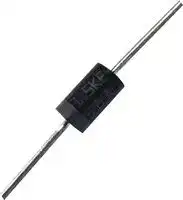
- Diode Case Style: DO-201AD
- Diode Configuration: Single
- Forward Voltage Max: 1.85V
- Forward Surge Current: 70A
- Reverse Recovery Time: 75ns
- Average Forward Current: 4A
- Operating Temperature Max: 175°C
- Repetitive Peak Reverse Voltage: 800V
| Delivery and price | |
|---|---|
| Units per pack | 4500 |
| Price | 0.238 € |
| Current stock | 10+ |
| Lead time | 30 days |
## MUR480EG, MUR4100EG

## SWITCHMODE Power Rectifiers

## **Ultrafast “E’’ Series with High Reverse Energy Capability**

These state−of−the−art devices are designed for use in switching power supplies, inverters and as free wheeling diodes.

## **Features**

- 20 mJ Avalanche Energy Guaranteed

- Excellent Protection Against Voltage Transients in Switching Inductive Load Circuits

**http://onsemi.com**

**ULTRAFAST RECTIFIER 4.0 AMPERES, 800−1000 VOLTS**

- Ultrafast 75 Nanosecond Recovery Time

- 175°C Operating Junction Temperature

- Low Forward Voltage

- Low Leakage Current

- High Temperature Glass Passivated Junction

- Reverse Voltage to 1000 V

- These are Pb−Free Devices*

## **Mechanical Characteristics:**

- Case: Epoxy, Molded

- Weight: 1.1 Gram (Approximately)

- Finish: All External Surfaces Corrosion Resistant and Terminal Leads are Readily Solderable

- Lead Temperature for Soldering Purposes: 260°C Max. for 10 Seconds

**AXIAL LEAD CASE 267 STYLE 1**

## **MARKING DIAGRAM**

- Shipped in Plastic Bags, 5,000 per Bag

- Available Tape and Reel, 1,500 per Reel, by Adding a “RL’’ Suffix to the Part Number

- Polarity: Cathode indicated by Polarity Band

**MAXIMUM RATINGS**

**Rating Symbol Value Unit** Peak Repetitive Reverse Voltage VRRM V Working Peak Reverse Voltage VRWM DC Blocking Voltage MUR480E VR 800 MUR4100E 1000 Average Rectified Forward Current(Square Wave; Mounting Method #3 Per Note 2) IF(AV) TA4.0 @ = 35 ° C A Non−Repetitive Peak Surge Current IFSM 70 A (Surge Applied at Rated Load Conditions Halfwave, Single Phase, 60 Hz) Operating Junction and Storage Temperature TJ, Tstg −65 to ° C Range +175 ~~=H~~ Stresses exceeding Maximum Ratings may damage the device. Maximum Ratings are stress ratings only. Functional operation above the Recommended Operating Conditions is not implied. Extended exposure to stresses above the Recommended Operating Conditions may affect device reliability.

A MUR 4xxx YYWW A = Assembly Location MUR4xxx = Device Number (see page 2) YY = Year WW = Work Week = Pb−Free Package (Note: Microdot may be in either location)

## **ORDERING INFORMATION**

See detailed ordering and shipping information on page 2 of this data sheet.

- *For additional information on our Pb−Free strategy and soldering details, please download the ON Semiconductor Soldering and Mounting Techniques Reference Manual, SOLDERRM/D.

Publication Order Number:

**1**

© Semiconductor Components Industries, LLC, 2013 **May, 2013 − Rev. 9**

**MUR480E/D**

**MUR480EG, MUR4100EG**

## **THERMAL CHARACTERISTICS**

|**THERMAL CHARACTERISTICS**||||
|---|---|---|---|
|**Rating**|**Symbol**|**Value**|**Unit**|
|Maximum Thermal Resistance, Junction−to−Ambient|R�JA|See Note 2|°C/W|


## **ELECTRICAL CHARACTERISTICS**

|**ELECTRICAL CHARACTERISTICS**||||
|---|---|---|---|
|**Characteristic**|**Symbol**|**Value**|**Unit**|
|Maximum Instantaneous Forward Voltage (Note 1)<br>(iF= 3.0 A, TJ= 150°C)<br>(iF= 3.0 A, TJ= 25°C)<br>(iF= 4.0 A, TJ= 25°C)|vF|1.53<br>1.75<br>1.85|V|
|Maximum Instantaneous Reverse Current (Note 1)<br>(Rated dc Voltage, TJ= 150°C)<br>(Rated dc Voltage, TJ= 25°C)|iR|900<br>25|�A|
|Maximum Reverse Recovery Time<br>(IF= 1.0 Amp, di/dt = 50 Amp/�s)<br>(IF= 0.5 Amp, iR= 1.0 Amp, IREC= 0.25 Amp)|trr|100<br>75|ns|
|Maximum Forward Recovery Time<br>(IF= 1.0 Amp, di/dt = 100 Amp/�s, Recovery to 1.0 V)|tfr|75|ns|
|Controlled Avalanche Energy (See Test Circuit in Figure 6)|WAVAL|20|mJ|
|Typical Peak Reverse Recovery Current<br>(IF= 1.0 A, di/dt = 50 A/�s)|IRM|2|A|


1. Pulse Test: Pulse Width = 300 � s, Duty Cycle � 2.0%.

## **ORDERING INFORMATION**

|**ORDERING INFORMATION**||||
|---|---|---|---|
|**Device**|**Marking**|**Package**|**Shipping**†|
|MUR480E|MUR480E|Axial Lead*|500 Units / Bulk|
|MUR480EG||Axial Lead*|500 Units / Bulk|
|MUR480ERL||Axial Lead*|1500 / Tape & Reel|
|MUR480ERLG||Axial Lead*|1500 / Tape & Reel|
|MUR480ES|MUR480ES|Axial Lead*|500 Units / Bulk|
|MUR480ESG||Axial Lead*|500 Units / Bulk|
|MUR4100E|MUR4100E|Axial Lead*|500 Units / Bulk|
|MUR4100EG||Axial Lead*|500 Units / Bulk|
|MUR4100ERL||Axial Lead*|1500 / Tape & Reel|
|MUR4100ERLG||Axial Lead*|1500 / Tape & Reel|


- †For information on tape and reel specifications, including part orientation and tape sizes, please refer to our Tape and Reel Packaging Specifications Brochure, BRD8011/D.

*This package is inherently Pb−Free.

**http://onsemi.com**

**2**

**MUR480EG, MUR4100EG**

## **MUR480EG, MUR4100EG**

**==> picture [489 x 624] intentionally omitted <==**

**----- Start of picture text -----**<br>
20 1000<br>400200200 T J  = 175°C°CC<br>10 TJ = 175°C 100°C 25°C 100402010402010201010 100°C°CC<br>7.0 4.0<br>2.0<br>5.0 1.0 25°C°CC<br>0.4<br>0.2<br>0.1<br>3.0 0.04 *<br>The curves shown are typical for the highest voltage<br>0.02<br>0.01 device in the voltage grouping. Typical reverse current<br>2.0 0.004 for lower voltage selections can be estimated from thesege selections can be estimated from thesee selections can be estimated from these<br>0.002 same curves if V R  is sufficiently below rated V R .<br>0.001<br>0 100 200 300 400 500 600 700 800 900 1000<br>1.0 VR, REVERSE VOLTAGE (VOLTS)R, REVERSE VOLTAGE (VOLTS), REVERSE VOLTAGE (VOLTS)<br>0.7 Figure 2. Typical Reverse Current*<br>0.5<br>0.3 10<br>Rated VR<br>0.2 8.0 R�JA = 28°C/W<br>0.1 6.0<br>0.07<br>4.0 dc<br>0.05<br>SQUARE WAVE<br>2.0<br>0.03<br>0.02 0<br>0 0.2 0.4 0.6 0.8 1.0 1.2 1.4 1.6 1.8 2 0 50 100 150 200 250<br>vF, INSTANTANEOUS VOLTAGE (VOLTS) TA, AMBIENT TEMPERATURE (°C)<br>Figure 1. Typical Forward Voltage Figure 3. Current Derating<br>(Mounting Method #3 Per Note 2)<br>10 70<br>9.0 TJ = 175J = 175= 175 ° C 60<br>50<br>8.0<br>5.0<br>7.0 40<br>TJ = 25°C<br>6.0<br>10 30<br>5.0 (Capacitive IPKPK =20<br>4.0 Load) IAVAV dc 20<br>3.0<br>SQUAREWAVE<br>2.0<br>10<br>1.0 9.0<br>8.0<br>0<br>7.0<br>0 1.0 2.0 3.0 4.0 5.0 0 10 20 30 40 50<br>IF(AV), AVERAGE FORWARD CURRENT (AMPS) , AVERAGE FORWARD CURRENT (AMPS) VR, REVERSE VOLTAGE (VOLTS)<br>�<br>, REVERSE CURRENT (   A)<br>IR<br>, INSTANTANEOUS FORWARD CURRENT (AMPS)<br>iF<br>, AVERAGE FORWARD CURRENT (AMPS)<br>IF(AV)<br>C, CAPACITANCE (pF)<br>, AVERAGE POWER DISSIPATION (WATTS)<br>PF(AV)<br>**----- End of picture text -----**<br>


**==> picture [245 x 171] intentionally omitted <==**

**----- Start of picture text -----**<br>
1000<br>400200200 T J  = 175°C°CC<br>100°C°CC<br>100402010402010201010<br>4.0<br>2.0<br>1.0 25°C°CC<br>0.4<br>0.2<br>0.1<br>0.04 *<br>The curves shown are typical for the highest voltage<br>0.02<br>0.01 device in the voltage grouping. Typical reverse current<br>for lower voltage selections can be estimated from thesege selections can be estimated from thesee selections can be estimated from these<br>0.004<br>0.002 same curves if V R  is sufficiently below rated V R .<br>0.001<br>0 100 200 300 400 500 600 700 800 900 1000<br>VR, REVERSE VOLTAGE (VOLTS)R, REVERSE VOLTAGE (VOLTS), REVERSE VOLTAGE (VOLTS)<br>�<br>, REVERSE CURRENT (   A)<br>IR<br>**----- End of picture text -----**<br>


**==> picture [239 x 175] intentionally omitted <==**

**----- Start of picture text -----**<br>
10<br>9.0 TJ = 175J = 175= 175 ° C<br>8.0<br>5.0<br>7.0<br>6.0<br>10<br>5.0 (Capacitive IPKPK =20<br>4.0 Load) IAVAV dc<br>3.0<br>SQUAREWAVE<br>2.0<br>1.0<br>0<br>0 1.0 2.0 3.0 4.0 5.0<br>IF(AV), AVERAGE FORWARD CURRENT (AMPS)<br>, AVERAGE POWER DISSIPATION (WATTS)<br>PF(AV)<br>**----- End of picture text -----**<br>


**Figure 4. Power Dissipation**

**Figure 5. Typical Capacitance**

**http://onsemi.com**

**3**

**MUR480EG, MUR4100EG**

**==> picture [493 x 203] intentionally omitted <==**

**----- Start of picture text -----**<br>
+VDD<br>IL 40 �H COIL<br>BVDUT<br>VD<br>ID<br>MERCURY<br>SWITCH ID<br>IL<br>DUT<br>S1<br>VDD<br>t0 t1 t2 t<br>**----- End of picture text -----**<br>


**Figure 6. Test Circuit**

**Figure 7. Current−Voltage Waveforms**

The unclamped inductive switching circuit shown in Figure 6 was used to demonstrate the controlled avalanche capability of the new “E’’ series Ultrafast rectifiers. A mercury switch was used instead of an electronic switch to simulate a noisy environment when the switch was being opened.

When S1 is closed at t0 the current in the inductor IL ramps up linearly; and energy is stored in the coil. At t1 the switch is opened and the voltage across the diode under test begins to rise rapidly, due to di/dt effects, when this induced voltage reaches the breakdown voltage of the diode, it is clamped at BVDUT and the diode begins to conduct the full load current which now starts to decay linearly through the diode, and goes to zero at t2.

By solving the loop equation at the point in time when S1 is opened; and calculating the energy that is transferred to the diode it can be shown that the total energy transferred is equal to the energy stored in the inductor plus a finite amount of energy from the VDD power supply while the diode is in breakdown (from t1 to t2) minus any losses due to finite

component resistances. Assuming the component resistive elements are small Equation (1) approximates the total energy transferred to the diode. It can be seen from this equation that if the VDD voltage is low compared to the breakdown voltage of the device, the amount of energy contributed by the supply during breakdown is small and the total energy can be assumed to be nearly equal to the energy stored in the coil during the time when S1 was closed, Equation (2).

The oscilloscope picture in Figure 8, shows the information obtained for the MUR8100E (similar die construction as the MUR4100E Series) in this test circuit conducting a peak current of one ampere at a breakdown voltage of 1300 V, and using Equation (2) the energy absorbed by the MUR8100E is approximately 20 mjoules.

Although it is not recommended to design for this condition, the new “E’’ series provides added protection against those unforeseen transient viruses that can produce unexplained random failures in unfriendly environments.

**==> picture [450 x 165] intentionally omitted <==**

**----- Start of picture text -----**<br>
EQUATION (1): CH1 500V A 20 � s 953 V VERT CHANNEL 2:<br>CH2 50mV IL<br>BVDUT 0.5 AMPS/DIV.<br>LI  [2]<br>WAVAL  � [1] 2 LPK [�] BVDUT–VDD �<br>CHANNEL 1:<br>VDUT<br>EQUATION (2): 500 VOLTS/DIV.<br>LI  [2]<br>WAVAL  � [1] 2 LPK<br>TIME BASE:<br>20 �s/DIV.<br>1 ACQUISITIO N S 217:33 HRS<br>SAVEREF SOU R CE STACK<br>CH1 CH2 REF REF<br>**----- End of picture text -----**<br>


**Figure 8. Current−Voltage Waveforms**

**http://onsemi.com**

**4**

# **MUR480EG, MUR4100EG**

# **NOTE 2 − AMBIENT MOUNTING DATA**

Data shown for thermal resistance junction−to−ambient (R�JA) for the mountings shown is to be used as typical guideline values for preliminary engineering or in case the tie point temperature cannot be measured.

**==> picture [495 x 608] intentionally omitted <==**

**----- Start of picture text -----**<br>
TYPICAL VALUES FOR R � JA IN STILL AIR<br>Mounting Lead Length, L (IN)<br>Method 1/8 1/4 1/2 3/4 Units<br>1 50 51 53 55 ° C/W<br>2 R � JA 58 59 61 63 ° C/W<br>3 28 ° C/W<br>MOUNTING METHOD 1<br>P.C. Board Where Available Copper<br>Surface area is small.<br>L L<br>ÉÉÉÉÉÉÉÉÉÉÉ<br>ÉÉÉÉÉÉÉÉÉÉÉ<br>MOUNTING METHOD 2<br>Vector Push−In Terminals T−28<br>ÉÉÉÉÉÉÉÉÉÉÉÉ L L<br>ÉÉÉÉÉÉÉÉÉÉÉÉ<br>MOUNTING METHOD 3<br>P.C. Board with<br>1−1/2 ″  x 1−1/2 ″  Copper Surface<br>ÉÉ<br>L = 1/2 ″<br>ÉÉ<br>ÉÉ<br>ÉÉ<br>ÉÉ<br>ÉÉ<br>Board Ground Plane<br>ÉÉ<br>ÉÉ<br>http://onsemi.com<br>5<br>**----- End of picture text -----**<br>


**MUR480EG, MUR4100EG**

## **PACKAGE DIMENSIONS**

**==> picture [232 x 145] intentionally omitted <==**

**----- Start of picture text -----**<br>
AXIAL LEAD<br>CASE 267−05<br>(DO−201AD)<br>ISSUE G<br>K A<br>D<br>1 2<br>re a<br>B<br>K<br>-|<br>**----- End of picture text -----**<br>


**==> picture [123 x 100] intentionally omitted <==**

**----- Start of picture text -----**<br>
NOTES:<br>1. DIMENSIONING AND TOLERANCING PER ANSI<br>Y14.5M, 1982.<br>2. CONTROLLING DIMENSION: INCH.<br>INCHES MILLIMETERS<br>DIM MIN MAX MIN MAX<br>A 0.287 0.374 7.30 9.50<br>B 0.189 0.209 4.80 5.30<br>D 0.047 0.051 1.20 1.30<br>EE K 1.000 --- 25.40 ---<br>STYLE 1:<br>PIN 1. CATHODE (POLARITY BAND)<br>2. ANODE<br>**----- End of picture text -----**<br>


**ON Semiconductor** and          are registered trademarks of Semiconductor Components Industries, LLC (SCILLC).  SCILLC owns the rights to a number of patents, trademarks, copyrights, trade secrets, and other intellectual property. A listing of SCILLC’s product/patent coverage may be accessed at www.onsemi.com/site/pdf/Patent−Marking.pdf.  SCILLC reserves the right to make changes without further notice to any products herein.  SCILLC makes no warranty, representation or guarantee regarding the suitability of its products for any particular purpose, nor does SCILLC assume any liability arising out of the application or use of any product or circuit, and specifically disclaims any and all liability, including without limitation special, consequential or incidental damages.  “Typical” parameters which may be provided in SCILLC data sheets and/or specifications can and do vary in different applications and actual performance may vary over time.  All operating parameters, including “Typicals” must be validated for each customer application by customer’s technical experts.  SCILLC does not convey any license under its patent rights nor the rights of others.  SCILLC products are not designed, intended, or authorized for use as components in systems intended for surgical implant into the body, or other applications intended to support or sustain life, or for any other application in which the failure of the SCILLC product could create a situation where personal injury or death may occur.  Should Buyer purchase or use SCILLC products for any such unintended or unauthorized application, Buyer shall indemnify and hold SCILLC and its officers, employees, subsidiaries, affiliates, and distributors harmless against all claims, costs, damages, and expenses, and reasonable attorney fees arising out of, directly or indirectly, any claim of personal injury or death associated with such unintended or unauthorized use, even if such claim alleges that SCILLC was negligent regarding the design or manufacture of the part.  SCILLC is an Equal Opportunity/Affirmative Action Employer.  This literature is subject to all applicable copyright laws and is not for resale in any manner.

## **PUBLICATION ORDERING INFORMATION**

## **LITERATURE FULFILLMENT** :

Literature Distribution Center for ON Semiconductor P.O. Box 5163, Denver, Colorado 80217 USA **Phone** : 303−675−2175 or 800−344−3860 Toll Free USA/Canada **Fax** : 303−675−2176 or 800−344−3867 Toll Free USA/Canada **Email** : orderlit@onsemi.com

**N. American Technical Support** : 800−282−9855 Toll Free USA/Canada

**ON Semiconductor Website** : **www.onsemi.com**

**Europe, Middle East and Africa Technical Support: Order Literature** : http://www.onsemi.com/orderlit Phone: 421 33 790 2910 **Japan Customer Focus Center** For additional information, please contact your local Phone: 81−3−5817−1050 Sales Representative

**http://onsemi.com**

**MUR480E/D**

**6**
Updated at April 14, 2026
onsemi is a premier global supplier of intelligent power and sensing technologies, driving disruptive innovations across the automotive, industrial, and cloud infrastructure markets. Recognized for their commitment to sustainability and reliable supply chains, the company accelerates advancements in vehicle electrification, industrial automation, and 5G networks by solving the industry's most complex design challenges. At the core of their portfolio is an industry-leading selection of discrete semiconductors. This extensive range features thousands of high-performance bipolar transistors, single and dual MOSFETs, and a comprehensive array of diodes, including Zener, Schottky, and fast-recovery rectifiers. Engineered for superior thermal performance and energy efficiency, these foundational components are critical for demanding power conversion, switching, and signal conditioning applications. Beyond essential discretes, onsemi provides a robust suite of advanced power management and circuit protection solutions. Their lineup includes intelligent power modules, single IGBTs, and transient voltage suppression (TVS) diodes designed to safeguard sensitive circuitry. Complimented by integrated passive filters, AC/DC LED driver ICs, and specialized sub-2.4GHz RF transceivers, onsemi equips engineers with the scalable, high-quality technologies needed to build a cleaner, smarter, and more connected world.
About Novapart
Novapart is a B2B electronic component broker specialising in stock shortages and cost reduction. We source hard-to-find parts and identify compliant alternatives across a catalogue of 410,000+ components from 500+ manufacturers.
Learn more →Stock Shortage Specialist
When a component is unavailable, discontinued or has an unacceptable lead time, we tap into our network of vetted European and Asian distributors to source what you need — without compromising on quality or traceability.
Request a quote →Compliant Alternatives
We identify pin-to-pin, electrically equivalent substitutes that meet the same certifications (RoHS, AEC-Q100, REACH) as your original specification — validated against datasheets, not just part numbers. Often at a lower cost.
BOM Analysis service →