
Image not available
Illustrative purposes only

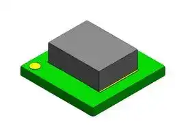
MUN3CAD03-SF
Non Isolated POL DC/DC Converter, ITE, Micro Module, 9.9 W, 600 mV, 3.3 V, 3 A
⚠️ Reference pricing provided. In case of supply shortages, we will connect you with our trusted procurement partners to ensure your project's continuity.
- Manufacturer: CYNTEC
- Product type: DC / DC Non Isolated Board Mount Converters - Adjustable Output
- SVHC: No SVHC (21-Jan-2025)
- Depth: 3mm
- Width: 3mm
- Height: 1.3mm
- Product Range: -
- Output Power Max: 9.9W
- Output Current Max: 3A
- Output Voltage Max: 3.3V
- Output Voltage Min: 600mV
- Input Voltage DC Max: 5.5V
- Input Voltage DC Min: 2.75V
- DC / DC Converter Type: Micro Module
- Power Supply Applications: ITE
- DC / DC Converter Output Type: Adjustable
| Delivery and price | |
|---|---|
| Units per pack | 500 |
| Price | 1.97 € |
| Current stock | 1000+ |
| Lead time | 30 days |
Datasheet

## **uPOL MODULE**
**3A, High Efficiency uPOL Module**
## **MUN3CAD03-SF**
## **FEATURES:**
- High Density uPOL Module
- 3A Output Current
- 94% Peak Efficiency at 5.0Vin to 3.3Vout
- Input Voltage Range from 2.75V to 5.5V
- Adjustable Output Voltage
- Enable / PGOOD Function
- Automatic Power Saving/PWM Mode
- Protections (UVLO,OCP: Non-latching, OTP)
- Internal Soft Start 0.8mS
- Compact Size: 3.0mm*3.0mm*1.3mm
- Pb-free for RoHS compliant
- 100% dropout voltage
- MSL 2, 260°C Reflow
## **GENERAL DESCRIPTION:**
The uPOL module is non-isolated dc-dc converters that can deliver up to 3A of output current. The PWM switching regulator, high frequency power inductor are integrated in one hybrid package. It only needs input/output capacitors and voltage dividing resistors.
The module has automatic operation with PWM mode and power saving mode according to loading, through constant on-time control, the module offers a simpler control loop and faster transient response. Other features include remote enable function, internal soft-start, nonlatching over current protection, power good, and input under voltage locked-out capability.
## **APPLICATIONS:**
- Single Li-Ion Battery-Powered Equipment
- Server power / telecom power
The low profile and compact size package (3.0mm× 3.0mmx 1.3mm) is suitable for automated assembly by standard surface mount equipment. The uPOL module is Pb-free and RoHS compliance.
- Cell Phones / PDAs / Palmtops
- SSD
## **TYPICAL APPLICATION CIRCUIT& PACKAGE:**
## **FIG.1 TYPICAL APPLICATION CIRCUIT**
**FIG.2 HIGH DENSITY LOW PROFILE**
**uPOL MODULE**
1 Rev. A2
## **MUN3CAD03-SF**
## **ORDER INFORMATION:**
||**Ambient Temp. Range**|**Package**|||
|---|---|---|---|---|
|**Part Number**|||**MSL**|**Note**|
||**(°C)**|**(Pb-Free)**|||
|MUN3CAD03-SF|-40 ~ +85|QFN|Level 2|-|
||||||
|**Order Code**||**Packing**||**Quantity**|
|MUN3CAD03-SF||Tape and reel||2000|
## **PIN CONFIGURATION:**
## **TOP VIEW**
## **PIN DESCRIPTION:**
|**Symbol**|**Pin No.**|**Description**|
|---|---|---|
|FB|1|Feedback input. Connect an external resistor divider from the output to<br>FB and FB to GND.|
|PG|2|Power Good indicator. The pin output is an open drain.|
|IN|3, 6, 10|Power input pin.|
|EN|4|Enable control. Do not be float.<br>EN = LOW, the module is off.<br>EN=HIGH, the module is on.|
|OUT|5|Power output pin.|
|GND|7|Power ground pin for signal, input, and output return path. This pin<br>needs to connect one or more ground plane directly.|
|LX|8, 9|Switch node, leave it no connection.|
2 Rev. A2
**MUN3CAD03-SF**
## **ELECTRICAL SPECIFICATIONS:** ~~eee~~
CAUTION: Do not operate at or near absolute maximum rating listed for extended periods of time. This stress may adversely impact product reliability and result in failures not covered by warranty.
|**Parameter**<br>~~ee~~|**Description**<br>~~ee~~|**Min.**|**Typ.**|**Max.**|**Unit**|
|---|---|---|---|---|---|
|<br>Absolute Maximum Ratings<br>~~ee ee~~<br>~~a~~<br>~~ee~~||||||
|VIN to GND<br>~~ee~~<br>~~ee~~||-|-|+6.0|V|
|VOUT to GND<br>~~ee~~<br>~~ee~~<br>~~ee~~||-|-|+6.0|V|
|SW to GND<br>~~ee~~<br>~~ee~~|Note 1|||VIN+0.3|V|
|EN to GND<br>~~ee~~<br>~~a~~<br>~~es~~|Note 1<br>~~es~~|-<br>~~es~~|-<br>~~es~~|+6.0<br>~~es~~|V<br>~~es~~|
|Tc<br>~~es~~<br>~~es~~|Case Temperature of Inductor<br>~~es~~<br>~~es~~|-<br>~~es~~<br>~~es~~|-<br>~~es~~<br>~~es~~|+110<br>~~es~~<br>~~es~~|°C<br>~~es~~<br>~~es~~|
|Tj<br>~~es~~<br>~~es~~<br>~~es~~|Junction Temperature<br>~~es~~<br>~~es~~<br>~~es~~|-40<br>~~es~~<br>~~es~~<br>~~es~~|-<br>~~es~~<br>~~es~~<br>~~es~~|+150<br>~~es~~<br>~~es~~<br>~~es~~|°C<br>~~es~~<br>~~es~~<br>~~es~~|
|Tstg<br>~~es~~<br>~~es~~|Storage Temperature<br>~~es~~<br>~~es~~|-40<br>~~es~~<br>~~es~~<br>~~es~~|-<br>~~es~~<br>~~es~~<br>~~es~~|+125<br>~~es~~<br>~~es~~|°C<br>~~es~~<br>~~es~~|
|ESD Rating<br>~~es~~|Human Body Model (HBM)<br>~~es~~<br>~~ee~~|-<br>~~es~~<br>~~ee~~<br>~~es~~<br>~~es~~|-<br>~~es~~<br>~~ee~~<br>~~es~~<br>~~ee~~|2k<br>~~es~~<br>~~ee~~<br>~~ee~~|V<br>~~es~~<br>~~ee~~|
||Machine Model (MM)<br>~~es~~|-<br>~~es ~~<br>~~es~~<br>~~es~~<br>~~es~~|-<br> ~~es~~<br>~~es~~<br>~~ee~~<br>~~ee~~|200<br>~~es~~<br>~~ee~~<br>~~ee~~|V<br>~~es~~|
||Charge Device Model (CDM)<br>~~es~~|-<br>~~es ~~<br>~~es~~<br>~~es~~|-<br> ~~ee ~~<br>~~es~~<br>~~ee~~|500<br> ~~ee~~<br>~~es~~<br>~~ee~~|V<br>~~es~~|
|<br>Recommendation Operating Ratings<br>~~es~~<br>~~es ee ee~~<br>~~a~~<br>~~ss~~||||||
|VIN<br>~~a~~<br>~~ss~~<br>~~rs~~|Input Supply Voltage<br>~~a~~<br>~~ss~~<br>|+2.75<br>~~a~~<br>~~ss~~<br>~~ss~~<br>~~es~~<br>|-<br>~~a~~<br>~~ss~~<br>~~ss~~<br>|+5.5<br>~~a~~<br>~~ss~~<br>|V<br>~~a~~<br>~~ss~~<br>|
|VOUT<br>~~ss~~<br>~~ss~~<br>~~rs~~|Adjusted Output Voltage<br>~~ss~~<br>~~ss~~<br>|+0.6<br>~~ss~~<br>~~ss~~<br>~~ss~~<br>~~es~~<br>|-<br>~~ss~~<br>~~ss~~<br>~~ss~~<br><br>~~es~~|+3.3<br>~~ss~~<br>~~ss~~<br>|V<br>~~ss~~<br>~~ss~~<br>|
|Ta<br>~~ss~~<br>~~rs~~|Ambient Temperature<br>~~ss~~<br>~~ss~~|-40<br>~~ss~~<br>~~es~~<br>~~ss~~|-<br>~~ss~~<br>~~ss~~<br>~~es~~|+85<br>~~ss~~<br>~~ss~~|°C<br>~~ss~~<br>~~ss~~|
|<br>Thermal Information<br>~~es~~<br>~~rsss~~<br>~~es~~<br>~~a~~<br>~~ee~~<br>~~eeeeeeee~~||||||
|Rth(jchoke-a)<br>~~a~~<br>~~ee~~|Thermal resistance from junction to<br>ambient,Ta = 25℃(Note 1)<br>~~a~~<br>~~ee~~|-<br>~~a~~<br>~~ee~~|45<br>~~a~~<br>~~ee~~|-<br>~~a~~<br>~~ee~~|°C/W<br>~~a~~<br>~~ee~~|
## NOTES:
1. Rth(jchoke-a) is measured with the component mounted on an effective thermal conductivity test board on 0 LFM condition. The test board size is 30mm× 30mm× 1.6mm with 4 layers, 2 oz per layer. The test condition is complied with JEDEC EIJ/JESD 51 Standards.
3 Rev. A2
**MUN3CAD03-SF**
~~ee~~ **ELECTRICAL SPECIFICATIONS:(Cont.)**
Conditions: TA = 25 ºC, unless otherwise specified. Test Board Information: 30mm×30mm×1.6mm, 4 layers 1 oz.
The output ripple and transient response measurement is short loop probing and 20MegHz bandwidth limited. Vin = 3.3V, Vout = 1.8V, Cin =22uF/6.3V/0805/X5R, Cout = 47uF/6.3V/0805/X5R, Cfb = 22pF/50V/0402/C0G, external +5V connect pull-up resister to PG, unless otherwise specified.
|**Symbol**<br>~~a~~<br>~~en~~|**Parameter**<br>~~ee~~<br>|**Conditions**<br>~~ee~~<br>|**Conditions**<br>~~ee~~<br>|**Min.**<br>~~ee~~<br>|**Typ.**<br>~~ee~~<br>|**Max.**<br>~~ee~~<br>|**Unit**<br>~~ee~~<br>|
|---|---|---|---|---|---|---|---|
|<br>Input Characteristics<br>~~a~~<br>~~eeee~~<br>~~en~~<br>~~eeee~~<br>~~a~~||||||||
|ISD<br>~~ena~~<br>~~a~~|Input shutdown<br>current<br>~~ee~~<br>|Vin=3.3V,EN = GND<br>~~ee~~<br>||-<br>~~ee~~<br>~~ee~~<br><br>~~ee~~|0.1<br>~~ee~~<br>~~ee~~<br><br>~~ee~~|1.0<br>~~ee~~<br>~~ee~~<br><br>~~ee~~|uA<br>~~ee~~<br>|
|IIN<br>~~a~~|Input supply<br>bias current<br>~~ee~~|Vin=3.3V, Iout=0A<br>Vout = 1.8V,EN = VIN<br>~~ee~~||-<br>~~ee~~<br>~~ee~~<br>~~ee~~<br>~~ee~~|100<br>~~ee ~~<br>~~ee~~<br>~~ee~~<br>~~ee~~|-<br> ~~ee~~<br>~~ee~~<br>~~ee~~<br>~~ee~~|uA<br>~~ee~~|
|IS|Input supply<br>current|Vin=3.3V, EN = VIN<br>~~es~~<br>~~ee~~||-<br>~~ee~~<br>~~es~~<br>~~ee~~<br>~~**e**e~~|-<br>~~ee ~~<br>~~es~~<br>~~ee~~<br>~~**e**e~~|-<br> ~~ee~~<br>~~es~~<br>~~ee~~<br>~~ee~~|-<br>~~es~~<br>~~**ee**~~|
|||Iout = 10mA<br>Vout = 1.8V<br>~~ee~~<br>~~ee~~||-<br>~~ee ~~<br>~~ee~~<br>~~**e**e~~|6.1<br> ~~ee~~<br>~~ee~~<br>~~**e**e~~<br>~~e~~|-<br>~~ee~~<br>~~ee~~<br>~~ee~~<br>~~e~~|mA<br>~~ee~~<br>~~**ee**~~|
|||Iout = 3.0A<br>Vout = 1.8V<br>~~ee~~||-<br>~~**e**e~~|1.83<br>~~**e**e~~<br>~~e~~|-<br>~~ee~~<br>~~e~~|A<br>~~**ee**~~|
|<br>Output Characteristics<br>~~**e**e ~~~~**e**e ee ~~~~**ee**~~<br>~~ee~~<br>~~e~~<br>~~ee~~||||||||
|IOUT(DC)<br>~~ee~~|Output current<br>~~ee~~|Vin=3.3V, Vout=1.8V<br>~~ee~~||0<br>~~ee~~|-<br>~~ee~~|3<br>~~ee~~|A<br>~~ee~~|
|VO(SET)<br>~~a~~|Ouput Voltage<br>Set Point<br>|With 0.1% tolerance for external<br>resistor used to set output<br>voltage at PWM mode<br>||-2.0<br>~~ee~~<br>|-<br>~~ee~~<br>|+2.0<br>~~ee~~<br>|% VO(SET)<br>~~ee~~<br>|
|ΔVOUT/ΔVIN<br>~~a~~<br>~~a~~|Line regulation<br>accuracy<br>~~ee~~<br>|Vin = 3.3V to 5V<br>Vout = 1.8V, Iout = 3A<br>~~ee~~<br>||-<br>~~ee~~<br>~~ee~~<br><br>~~ee~~|0.5<br>~~ee~~<br>~~ee~~<br><br>~~ee~~|-<br>~~ee~~<br>~~ee~~<br>|% VO(SET)<br>~~ee~~<br>~~ee~~<br>|
|ΔVOUT/ΔIOUT<br>~~a~~<br>~~a~~|Load regulation<br>accuracy<br>~~ee~~<br>~~ee~~|Iout = 0A to 3A<br>Vin = 3.3V, Vout = 1.8V<br>~~ee~~<br>~~ee~~||-<br>~~ee~~<br>~~ee~~<br>~~ee~~<br>~~ee~~|3<br>~~ee~~<br>~~ee~~<br>~~ee~~<br>~~ee~~|-<br>~~ee~~<br>~~ee~~<br>~~ee~~|% VO(SET)<br>~~ee~~<br>~~ee~~<br>~~ee~~|
|VOUT(AC)<br>~~a~~|Output ripple<br>voltage<br>~~ee~~|Vin = 3.3V,<br>Vout = 1.8V<br>EN = VIN<br>~~ee~~|Iout = 0A<br>~~ee~~|-<br>~~ee ~~<br>~~ee~~<br>~~ee~~|15<br> ~~ee~~<br>~~ee~~<br>~~ee~~|-<br>~~ee~~<br>~~ee~~|mVp-p<br>~~ee~~<br>~~ee~~|
||||Iout = 3A<br>~~re~~|-<br>~~re~~<br>~~ee~~|15<br>~~ee~~<br>~~ee~~|-<br>~~ee~~<br>~~ee~~|mVp-p<br>~~ee~~|
|COUT(MAX)<br>~~a~~|Maximum<br>capacitive load<br>~~ee~~|Iout = 3A, ESR≧1m<br>~~ee~~||-<br>~~ee~~<br>~~ee~~|-<br>~~ee~~<br>~~ee~~|150<br>~~ee~~<br>~~ee~~|uF<br>~~ee~~|
4 Rev. A2
**MUN3CAD03-SF**
~~ee~~ **ELECTRICAL SPECIFICATIONS:(Cont.)**
Conditions: TA = 25 ºC, unless otherwise specified. Test Board Information: 30mm×30mm×1.6mm, 4 layers 1 oz.
The output ripple and transient response measurement is short loop probing and 20MegHz bandwidth limited. Vin = 3.3V, Vout = 1.8V, Cin =22uF/6.3V/0805/X5R, Cout = 47uF/6.3V/0805/X5R, Cfb = 22pF/50V/0402/C0G, external +5V connect pull-up resister to PG, unless otherwise specified.
|**Symbol**<br>~~a~~|**Parameter**<br>~~ee~~|**Conditions**<br>~~e~~|**Min.**<br>~~e~~~~**e**~~|**Typ.**<br>~~**e**~~<br>~~e~~|**Max.**<br>~~**e**~~|**Unit**<br>~~**e**~~|
|---|---|---|---|---|---|---|
|<br>Control Characteristics<br>~~a~~<br>~~eee~~~~**e**~~<br>~~e~~<br>~~ee~~|||||||
|VEN_TH<br>~~ee~~<br>~~pe~~<br>~~a~~<br>~~a~~|Enable upper<br>threshold voltage<br>~~ee~~<br>~~pe~~<br>~~ee~~<br>|VEN_THrising<br>~~ee~~<br>~~pe~~<br>~~ee~~|1.2<br>~~ee~~<br>~~pe~~<br>~~ee~~|-<br>~~ee~~<br>~~pe~~<br>~~ee~~|-<br>~~ee~~<br>~~pe~~<br>~~ee~~|V<br>~~ee~~<br>~~pe~~|
||Enable lower<br>threshold voltage<br>~~pe~~<br>~~ee~~<br>~~a~~<br>|VEN_THfalling<br>~~pe~~<br>~~ee~~<br>~~ee~~<br>|-<br>~~pe~~<br>~~ee~~<br>~~ee~~<br>|-<br>~~pe~~<br>~~ee~~<br>~~ee~~<br>|0.4<br>~~pe~~<br>~~ee~~<br>|V<br>~~pe~~<br>|
|FOSC<br>~~a ~~<br>~~a~~<br>~~a~~|Oscillator<br>frequency<br>~~ee~~<br> ~~a~~<br><br>|PWM Operation<br>~~ee ~~<br>~~ee~~<br><br>|0.96<br> ~~ee~~<br>~~ee~~<br><br>|1.2<br>~~ee ~~<br>~~ee~~<br><br>~~ee eee~~<br>|1.44<br> ~~ee~~<br><br>~~eee~~<br>|MHz<br><br>~~eee~~<br>|
|VPGOOD_TH<br> <br>~~a ee~~<br>~~a~~<br>~~a~~|PGOOD high<br> ~~a~~<br>~~ee~~<br>|Respect the VREF<br>~~ee ~~<br>~~ee~~<br>|-<br> ~~ee~~<br>~~ee~~<br><br>~~ee~~|90<br>~~ee~~<br>~~ee~~<br>~~ee eee~~<br><br>~~ee~~|-<br>~~ee~~<br>~~eee~~<br><br>~~ee~~|%<br>~~ee~~<br>~~eee~~<br>|
|VPGOOD_LV<br>~~a~~<br>~~a~~<br>~~en~~|PGOOD logic low<br>voltage<br>~~ee~~<br>~~ee~~|IPGOOD= 4mA<br>~~ee~~<br>~~ee~~|0.04<br>~~ee~~<br>~~ee~~<br>~~ee~~|0.15<br>~~ee eee~~<br>~~ee~~<br>~~ee~~<br>~~ee~~|0.3<br>~~eee~~<br>~~ee~~<br>~~ee~~<br>~~ee~~|V<br>~~eee~~<br>~~ee~~<br>~~ee~~|
|Discharge<br>~~a~~<br>~~en~~|LX node discharge<br>resister<br>~~ee~~|LX node discharge<br>~~ee~~|-<br>~~ee~~<br>~~ee~~|50<br>~~ee ~~<br>~~ee~~|-<br> ~~ee~~<br>~~ee~~|ohm<br>~~ee~~|
|<br>Fault Protection<br>~~eeee~~<br>~~en~~<br>~~ee~~<br>~~a~~|||||||
|ILIMIT_TH<br>~~en~~<br>~~a~~<br>~~a~~<br>~~a~~|Current limit<br>threshold<br>~~ee~~<br>~~ee~~<br>~~ee~~<br>|Peak value of output current<br>~~ee~~<br>~~ee~~<br>~~es~~<br>|5.0<br>~~ee~~<br>~~ee~~<br>~~ee~~<br>|-<br>~~ee~~<br>~~ee~~<br>|7.0<br>~~ee~~<br>~~ee~~<br>|A<br>~~ee~~<br>~~ee~~<br>|
|TOTP<br>~~a~~<br>~~a~~<br>~~a~~|Over temperature<br>protection<br>~~ee~~<br>~~ee~~<br>|~~ee~~<br>~~es~~<br>|-<br>~~ee~~<br>~~ee~~<br><br>~~ee~~|150<br>~~ee~~<br><br>~~ee~~|-<br>~~ee~~<br>|°C<br>~~ee~~<br>|
|UVLO<br>~~a~~<br>~~a ee~~|Under voltage<br>lockout<br>~~ee~~<br>~~ee~~|~~es~~<br>~~ee~~|~~ee~~<br>~~ee~~<br>~~ee~~|2.7<br>~~ee~~<br>~~ee~~|~~ee~~|V<br>~~ee~~|
5 Rev. A2
**MUN3CAD03-SF**
## **TYPICAL PERFORMANCE CHARACTERISTICS: (1.0 VOUT)**
Conditions: TA = 25 ºC, unless otherwise specified. Test Board Information: 30mm×30mm×1.6mm, 4 layers 2oz.
The output ripple and transient response measurement is short loop probing and 20MegHz bandwidth limited. Cin =22uF/6.3V/0805/X5R, Cout = 47uF/6.3V/0805/X5R, Cfb = 22pF/50V/0402/C0G, external +5V connect pullup resister to PG, unless otherwise specified.
The following figures provide the typical characteristic curves at 1.0Vout.
**==> picture [374 x 334] intentionally omitted <==**
**----- Start of picture text -----**<br>
FIG.3 EFFICIENCY V.S. LOAD CURRENT FIG.4 DE-RATING CURVE<br>———————— Tek Stop i<br>ha in in Pag | "an Non hi soll Kael TI itll eae |<br>Gauls: : : anes<br>100ms 10.0kKS/s @, 400ns 2.50GS/s<br>value_11.6mV DLMean9.98m 4.00mMin Max1.6m10k pointsStd2.25mDev___3.60mv (@_io.omvvyPeak—-Peak Value14.4mV Meant0.00000s__12.0m Min0.00 Max68.8m10k points Std<br>FIG.5 OUTPUT RIPPLE FIG.6OUTPUT RIPPLE<br>(3.3VIN, IOUT=0A) (3.3VIN, IOUT=3A)<br>- Tek Stop =<br>PG<br>Seeeeeenae<br>VIN<br>Sera eee dovertaghanmihn<br>50.0mvw 100ys 10.0MS/s @, :xual VOUT een<br>Value_46.0mV 2.00A40.6mMean2 _ jiiev248.800usMin0.00 Max176m10k pointsStd15.1mDev2.92A @@ sooviov s% @ ) 400pusGi 224.0008 _ 10k2.50MS/spoints<br>FIG.7 TRANSIENT RESPONSE FIG.8 TURN-ON<br>(3.3VIN, 50% to 100% LOAD STEP) (3.3VIN, IOUT=3A)<br>**----- End of picture text -----**<br>
6 Rev. A2
**MUN3CAD03-SF**
## **TYPICAL PERFORMANCE CHARACTERISTICS: (1.8VOUT)**
Conditions: TA = 25 ºC, unless otherwise specified. Test Board Information: 30mm×30mm×1.6mm, 4 layers 2oz.
The output ripple and transient response measurement is short loop probing and 20MegHz bandwidth limited. Cin =22uF/6.3V/0805/X5R, Cout = 47uF/6.3V/0805/X5R, Cfb = 22pF/50V/0402/C0G, external +5V connect pullup resister to PG, unless otherwise specified.
The following figures provide the typical characteristic curves at 1.8Vout.
**==> picture [377 x 334] intentionally omitted <==**
**----- Start of picture text -----**<br>
FIG.9 EFFICIENCY V.S. LOAD CURRENT FIG.10 DE-RATING CURVE<br>ij Tek Stop it<br>Nit pate ain ("te iia: H , |<br>id20.0msv0.000005 51 0 .0kS/sK points _3.60mv@s (@ i0.0omves dit400ns 0.00000 5 2.50GS/s10k points<br>value_11.2mV Mean15.1m Min11.2m Max19.2m Std4.24m Dev Peak—Peak Value_15.2mV Mean14.8m Min0.00 Max18.8m Std<br>FIG.11 OUTPUT RIPPLE FIG.12 OUTPUT RIPPLE<br>(3.3VIN, IOUT=0A) (3.3VIN, IOUT=3A)<br>= Tek Stop =<br>PG<br>:—<br>VIN<br>a BED rosin<br>VOUT<br>4<br>@50.0mvvy 100ys 10.0MS/s @s<br>2.00A 2 _)\iiev248.800us 10k points 2.92A @ i0v % @ 400us 2.50MS/s<br>value_74.0mV 83.3mMean 0.00Min Max176m Std44.5m Dev @ 5.00v_ % Ge*456.000us 10k points<br>FIG.13 TRANSIENT RESPONSE FIG.14 TURN-ON<br>(3.3VIN, 50% to 100% LOAD STEP) (3.3VIN, IOUT=3A)<br>**----- End of picture text -----**<br>
7 Rev. A2
**MUN3CAD03-SF**
## **TYPICAL PERFORMANCE CHARACTERISTICS: (3.3VOUT)**
Conditions: TA = 25 ºC, unless otherwise specified. Test Board Information: 30mm×30mm×1.6mm, 4 layers 2oz.
The output ripple and transient response measurement is short loop probing and 20MegHz bandwidth limited. Cin =22uF/6.3V/0805/X5R, Cout = 47uF/6.3V/0805/X5R, Cfb = 22pF/50V/0402/C0G, external +5V connect pullup resister to PG, unless otherwise specified.
The following figures provide the typical characteristic curves at 3.3Vout.
**==> picture [380 x 334] intentionally omitted <==**
**----- Start of picture text -----**<br>
FIG.15 EFFICIENCY V.S. LOAD CURRENT FIG.16 DE-RATING CURVE<br>it Tek Stop it<br>PEEee fg Ml | | ly , ae wt| me A,a. Al.‘i<br>ioomves id v0.000005 10 0kS/sk points _3.60mv@rs: (@_ i0.0omves ——_dév0.000005 2.50GS/s_10k points<br>value_12.0mV Mean13.2m Min1.6m 20.8mMax Std2.83mDev Peak-Peak value_16.4mV Mean12.6m Min0.00 Max68.8m Std<br>FIG.17 OUTPUT RIPPLE FIG.18 OUTPUT RIPPLE<br>(5.0VIN, IOUT=0A) (5.0VIN, IOUT=3A)<br>= Tek Stop =<br>PG<br>Sone mere<br>ae "sis har iesd ta shiner<br>VIN<br>VOUT<br>1D<br>50.0mvvwy 100ys 10.0MS/s @s<br>2.00A Q Ji 248 S00us 10k points 2.92A @ i.00v %& @ 400ps 2.S0MS/s<br>Value Mean Min Max Std Dev @ 5.00v %& iey708.000us 10k points<br>Peak-Peak _106mV 96.9m 0.00 176m 49.7m<br>FIG.19 TRANSIENT RESPONSE FIG.20 TURN-ON<br>(5.0VIN, 50% to 100% LOAD STEP) (5VIN, IOUT=3A)<br>**----- End of picture text -----**<br>
8 Rev. A2
## **MUN3CAD03-SF**
**APPLICATIONS INFORMATION:** ~~eee~~
## **SAFETY CONSIDERATIONS:**
Certain applications and/or safety agencies may require fuses at the inputs of power conversion components. Fuses should also be used when there is the possibility of sustained input voltage reversal which is not current limited. For greatest safety, we recommend a fast blow fuse installed in the ungrounded input supply line. The installer must observe all relevant safety standards and regulations. For safety agency approvals, install the converter in compliance with the end-user safety standard.
## **INPUT FILTERING:**
The module should be connected to as low AC impedance source supply and a highly inductive source or line inductance can affect the stability of the module. Input capacitors must be placed directly to the input pin of the module, to minimize input ripple voltage and ensure module stability.
## **OUTPUT FILTERING:**
To reduce output ripple and improve the dynamic response to as step load change, the additional capacitors at the output must be used. Low ESR ceramic capacitors are recommended to improve the output ripple and dynamic response of the module.
## **PROGRAMMING OUTPUT VOLTAGE:**
The output voltage can be programmed by the dividing resistor RFB_top and RFB_bot, Assume RFB_top set 200 Kohm, the output voltage can be calculated as shown in Equation 1 and the resistance according to typical output voltage is shown in TABLE 1.
VOUT (V) 6.0 1 RFB_top RFB_bot
**==> picture [34 x 9] intentionally omitted <==**
|VOUT|<br><br><br>RFB_bot<br>1<br>6.0<br>(V)<br>VOUT|<br><br>RFB_bot|
|---|---|---|
|Vout (V)|RFB_top (k)|RFB_bot(k)|
|1.0|200|300|
|1.2|200|200|
|1.8|200|100|
|2.5|200|63.158|
|3.3|200|44.444|
**TABLE.1 RESISTOR VALUES FOR COMMON OUTPUTVOLTAGES**
9 Rev. A2
**MUN3CAD03-SF**
~~hs~~ **APPLICATIONS INFORMATION: (Cont.)**
## **LOAD TRANSIENT RESPONSE INCREASE:**
In some applications, adding a ceramic cap (CFB) in parallel with RFB-top may further speedy up the load transient responses, recommend capacitance as below table 2.
|Vout (V)|CFB (pF)|
|---|---|
|1.0|22~100|
|1.2|22~100|
|1.8|22~100|
|2.5|22~47|
|3.3|22|
**TABLE.2 RECOMMEND CFB FOR LOAD TRANSIENT**
## **THERMAL CONSIDERATIONS:**
All of thermal testing condition is complied with JEDEC EIJ/JESD 51 Standards. Therefore, the test board size is 30mm×30mm×1.6mm with 4 layers 2oz. The case temperature of module sensing point is shown as FIG.21 Then Rth(jchoke-a) is measured with the component mounted on an effective thermal conductivity test board on 0 LFM condition. The module is designed for using when the case temperature is below 110°C regardless the change of output current, input/output voltage or ambient temperature.
## **Sensing point (Defined case temperature)**
**FIG.21 CASE TEMPERATURE SENSING POINT**
10 Rev. A2
**MUN3CAD03-SF**
## **APPLICATIONS INFORMATION: (Cont.)**
## **LAYOUT RECOMMENDATIONS:**
**FIG.22 CIRCUIT OF LAYOUT**
**FIG.23 LAYOUT OF FIRST LAYER**
11 Rev. A2
## **MUN3CAD03-SF**
## **APPLICATIONS INFORMATION: (Cont.)**
## **REFLOW PARAMETERS:**
Lead-free soldering process is a standard of electronic products production. Solder alloys like Sn/Ag, Sn/Ag/Cu and Sn/Ag/Bi are used extensively to replace the traditional Sn/Pb alloy. Sn/Ag/Cu alloy (SAC) is recommended for this power module process. In the SAC alloy series, SAC305 is a very popular solder alloy containing 3% Ag and 0.5% Cu and easy to obtain. Figure 24 shows an example of the reflow profile diagram. Typically, the profile has three stages. During the initial stage from room temperature to 150°C, the ramp rate of temperature should not be more than 3°C/sec. The soak zone then occurs from 150°C to 200°C and should last for 60 to 120 seconds. Finally, keep at over 217°C for 60~150 seconds limit to melt the solder and make the peak temperature at the range from 255°C to 260°C (Do not exceed 30 sec). It is noted that the time of peak temperature should depend on the mass of the PCB board. The reflow profile is usually supported by the solder vendor and one should adopt it for optimization according to various solder type and various manufacturers’ formulae.
**FIG.36 RECOMMENDATION REFLOW PROFILE***
## **(Not to scale)**
## ***Refer to the Classification Reflow Profile of J-STD-020.**
12 Rev. A2
## **MUN3CAD03-SF**
## **PACKAGE OUTLINE DRAWING:**
## Unit: mm
13 Rev. A2
**MUN3CAD03-SF**
**==> picture [458 x 595] intentionally omitted <==**
**----- Start of picture text -----**<br>
LAND PATTERN REFERENCE:<br>eee<br> Unit: mm<br>-———_ 2.300 ———<br>0.600 —+ 0.600<br>aso *— 0.960+ | vo |<br>3.000 _ |__| + aot L a<br>St OF<br>0 of slow<br>RECOMMENDED LAND PATTERN<br>a 2.200|<br>0.330<br>0.520 k—++— 0.400<br>oT<br>2.700 _ [| 0.260— — »——— “re0.900<br>Cd iL! ‘i<br>0.400 = 0.300<br>2.700<br>RECOMMENDED STENCIL PATTERN<br>BASED ON 0.1mm THICKNESS STENCIL (Reference only)<br>**----- End of picture text -----**<br>
14 Rev. A2
## **MUN3CAD03-SF**
## **PACKING REFERENCE:**
|Unit: mm||||||||
|---|---|---|---|---|---|---|---|
||||**Package In Tape Loading Orientation**|**Package In Tape Loading Orientation**||||
||||Pini|Sprocket hole||||
||||Po<br>‘OL|||||
||||**Tape Dimension**|||||
|Do<br>Po<br>i|||P2<br>B<br>a<br>:|||=||
||<br>& oP<br>0 P}O 0:0<br>0 4<br>5'(MAX)<br>_<br>=<br>supEHoemeeF|<br>«7h<br>:<br>|<br>;<br>D1<br>~B<br>Pulling Direction||||||||
||A0||3.200.10<br>E1||||1.750.10|
||B0||3.300.10<br>K0||||1.650.10|
||F||5.500.05<br>P0||||4.000.10|
||W||12.000.30<br>P1||||4.000.10|
||D0||φ1.550.05<br>P2||||2.000.05|
||D1||φ1.5 +0.1/-0<br>T||||0.250.10|
15 Rev. A2
## **MUN3CAD03-SF**
## **PACKING REFERENCE: (Cont.)**
**==> picture [334 x 177] intentionally omitted <==**
**----- Start of picture text -----**<br>
Unit: mm<br>Reel Dimension<br>See Detail A<br>Detail A<br>**----- End of picture text -----**<br>
## **Peel Strength of Top Cover Tape**
The peel speed shall be about 300mm/min.
The peel force of top cover tape is between 0.1N to 1.3N
16 Rev. A2
**MUN3CAD03-SF**
## **REVISION HISTORY:** ~~hee~~
|**Date**|**Revision**|**Changes**|
|---|---|---|
|2017.05.18|P00|Release the preliminary specification.|
|2017.08.03|P01|1、<br>Add page 3 Thermal Information<br>2、<br>Add page 4~5 electrical specifications<br>3、<br>Add page 6~8 1.0Vo、1.8Vo and 3.3Vo characteristics<br>4、<br>Add page 9~12 applications information<br>5、<br>Add page 14 land pattern reference|
|2019.06.24|P02|1、<br>Modified packing information for tape reel<br>(page.16~17)|
|2019.07.23|A0|1、<br>Update page 2 packing quantity form 1000 to 2000<br>pcs|
|2022.02.04|A1|2、<br>Update page 14 land pattern reference|
|2023.10.25|A2|1. Update outline drawing<br>2. Update recommended reflow parameters.|
17 Rev. A2
Updated at June 9, 2026
About Novapart
Novapart is a B2B electronic component broker specialising in stock shortages and cost reduction. We source hard-to-find parts and identify compliant alternatives across a catalogue of 410,000+ components from 500+ manufacturers.
Learn more →Stock Shortage Specialist
When a component is unavailable, discontinued or has an unacceptable lead time, we tap into our network of vetted European and Asian distributors to source what you need — without compromising on quality or traceability.
Request a quote →Compliant Alternatives
We identify pin-to-pin, electrically equivalent substitutes that meet the same certifications (RoHS, AEC-Q100, REACH) as your original specification — validated against datasheets, not just part numbers. Often at a lower cost.
BOM Analysis service →