
Image not available
Illustrative purposes only

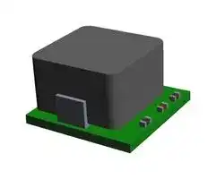
MUN12AD03-SM
DC-DC Converter, Non-Isolated, Micro Module, Adjustable, 4.5V to 16V, 3A
⚠️ Reference pricing provided. In case of supply shortages, we will connect you with our trusted procurement partners to ensure your project's continuity.
- Manufacturer: CYNTEC
- Product type: DC / DC Non Isolated Board Mount Converters - Adjustable Output
- SVHC: No SVHC (21-Jan-2025)
- Depth: 6mm
- Width: 6mm
- Height: 3.5mm
- Product Range: -
- Output Power Max: 15W
- Output Current Max: 3A
- Output Voltage Max: 5V
- Output Voltage Min: 600mV
- Input Voltage DC Max: 16V
- Input Voltage DC Min: 4.5V
- DC / DC Converter Type: Micro Module
- Power Supply Applications: Communications Equipment, Networking Equipment, Servers and Storage Equipments
- DC / DC Converter Output Type: Adjustable
| Delivery and price | |
|---|---|
| Units per pack | 500 |
| Price | 3.2 € |
| Current stock | 1000+ |
| Lead time | 30 days |
Datasheet

## **uPOL Module** ## **3A, High Efficiency uPOL Module** **MUN12AD03-SM** ## **FEATURES:** - High Density uPOL Module - 3A Output Current - Input Voltage Range from 4.5V to 16V - Output Voltage Range from 0.6V to 5.0V - 93% Peak Efficiency at 12VIN - Enable / PGOOD Function - Automatic Power Saving/PWM Mode - Protections (OCP: Non-latching, OTP) - Internal Soft Start - Compact Size: 6mm*6mm*3.5mm(Max) - Pb-free for RoHS compliant ## **GENERAL DESCRIPTION:** The uPOL module is non-isolated dc-dc converters that can deliver up to 3A of output current. The PWM switching regulator, high frequency power inductor are integrated in one hybrid package. It only needs input/output capacitors and one voltage dividing resistor. The module has automatic operation with PWM mode and power saving mode according to loading. Other features include remote enable function, internal soft-start, non-latching over current protection and power good. - MSL 2, 250°C Reflow ## **APPLICATIONS:** - Distributed Power Supply - Server, Workstation, and Storage The low profile and compact size package (6.0mm × 6.0mm x 3.5mm) is suitable for automated assembly by standard surface mount equipment. The uPOL module is Pb-free and RoHS compliance. - Networking and Datacom ## **TYPICAL APPLICATION CIRCUIT & PACKAGE SIZE:** **==> picture [458 x 287] intentionally omitted <==** **----- Start of picture text -----**<br> VBias<br>EN<br>R PG VPGOOD<br>EN PGOOD<br>VIN VOUT 3.5 mm<br>VIN Vout<br>uPOL Module (Max)<br>C IN SS FB C OUT<br>6.0mm<br>C SS GND R FB 6.0mm<br>co ®<br>TABLE 1: OUTPUT VOLTAGE SETTING<br>Vout 1.0V 1.2V 1.8V 2.5V 3.3V 5.0V<br>RFB (Ohm) 150k 100k 49.9k 31.6k 22.1k 13.7k<br>eeeenee<br>1 Rev. A1<br>**----- End of picture text -----**<br> ## **MUN12AD03-SM** ## **ORDER INFORMATION:** |**Part Number**|**Operating Temperature**<br>**Range (°C)**|**Package**<br>**(Pb-Free)**|**MSL**|**Note**| |---|---|---|---|---| |MUN12AD03-SM|MUN12AD03-SM<br>-40 ~ +125|QFN|Level 2|-| |**Order Code**|**Packing**|**Quantity**| |---|---|---| |MUN12AD03-SM|Tape and reel|1000| ## **PIN CONFIGURATION:** **==> picture [69 x 11] intentionally omitted <==** **----- Start of picture text -----**<br> TOP VIEW<br>**----- End of picture text -----**<br> 2 Rev. A1 **MUN12AD03-SM** ## **PIN DESCRIPTION:** ~~ee~~ |**Symbol**|**Pin No.**|**Description**| |---|---|---| |VIN|1, 19, 20|Power input pin. It needs to connect input rail and thermal exposed pad<br>of VIN_TPD(21) for heat transferring. Place the input ceramic type<br>capacitor as closely as possible to this pin. One capacitor of 22uF at least<br>for input capacitance.| |PHASE|2, 3, 4|Switch output. Connect to thermal exposed pad of PHASE_TPD(22) for<br>heat transferring.| |GND|5, 6, 7|Power ground pin for signal, input, and output return path. This pin<br>needs to connect one or more ground plane directly. Connect to thermal<br>exposed pad of GND_TPD(23, 25) for heat transferring.| |FB|9|Feedback input. Connect an external resistor divider from the FB to GND<br>to set the output voltage.| |VOUT|10, 11, 12,<br>13, 14|Power output pin. Connect to output and thermal exposed pad of<br>VOUT_TPD(24) for heat transferring. Place the output capacitors as<br>closely as possible to this pin. Two capacitors of 47uF at least for output<br>capacitance.| |SS|15|Soft start pin. It has internal current source for changing ramp up to set<br>soft start time. Leave SS pin floating for default 1ms soft-start time.| |N.C.|8,16|Not Connected.| |PGOOD|17|Power good signal pin. Open drain output when the output voltage is<br>above 90% of regulation point.| |EN|18|On/Off control pin for module.| |VIN_TPD|21|Power input pin. Connect input rail and using for heat transferring to heat<br>dissipation layer by Vias connection.| |PHASE_TPD|22|Phase node pin. Using for heat transferring to heat dissipation layer by<br>Vias connection.| |GND_TPD|23, 25|Power ground pin. It needs to connect one or more ground plane directly<br>and using for heat transferring to heat dissipation layer by Vias<br>connection.| |VOUT_TPD|24|Power output pin. Connect to output and using for heat transferring to<br>heat dissipation layer by Vias connection.| 3 Rev. A1 **MUN12AD03-SM** ## **ELECTRICAL SPECIFICATIONS:** ~~ee~~ CAUTION: Do not operate at or near absolute maximum rating listed for extended periods of time. This stress may adversely impact product reliability and result in failures not covered by warranty. |**Parameter**<br>~~a~~|**Description**<br>~~ee~~|**Min.**<br>~~ee~~|**Typ.**<br>~~ee~~|**Max.**<br>~~ee~~|**Unit**<br>~~ee~~| |---|---|---|---|---|---| |◼<br>Absolute Maximum Ratings<br>~~aee~~<br>~~ee~~|||||| |VIN to GND<br>~~ee~~<br>~~es~~<br>~~es~~|~~ee~~<br>~~es~~<br>~~ss~~|-<br>~~ee~~<br>~~es~~<br>~~ss~~|-<br>~~ee~~<br>~~es~~<br>~~ss~~|+18<br>~~ee~~<br>~~es~~<br>~~ss~~|V<br>~~ee~~<br>~~es~~<br>~~ss~~| |VOUT to GND<br>~~es~~<br>~~Rs~~|~~ss~~<br>~~ss~~|-<br>~~ss~~<br>~~ss~~|-<br>~~ss~~<br>~~ss~~|+6.5<br>~~ss~~<br>~~ss~~|V<br>~~ss~~<br>~~ss~~| |EN to GND<br>~~es~~<br>~~Rs~~<br>~~es~~|~~ss~~<br>~~ss~~<br>~~es~~|-<br>~~ss~~<br>~~ss~~<br>~~es~~<br>~~ss~~|-<br>~~ss~~<br>~~ss~~<br>~~es~~<br>~~ss~~|VIN+0.3<br>~~ss~~<br>~~ss~~<br>~~es~~|V<br>~~ss~~<br>~~ss~~<br>~~es~~| |Tc<br>~~Rs~~<br>~~es~~|Case Temperature of Inductor<br>~~ss~~<br>~~es~~|-<br>~~ss~~<br>~~es~~<br>~~ss~~|-<br>~~ss~~<br>~~es~~<br>~~ss~~|+110<br>~~ss~~<br>~~es~~|°C<br>~~ss~~<br>~~es~~| |Tj<br>~~es~~<br>~~ee~~|Junction Temperature<br>~~es~~<br>~~ee~~|-40<br>~~es~~<br>~~ss~~<br>~~ee~~|-<br>~~es~~<br>~~ss~~<br>~~ee~~|+150<br>~~es~~<br>~~ee~~|°C<br>~~es~~<br>~~ee~~| |Tstg<br>~~a~~|Storage Temperature<br>~~a~~|-40<br>~~a~~|-<br>~~a~~|+125<br>~~a~~|°C<br>~~a~~| |◼<br>Recommendation Operating Ratings<br>~~|~~|||||| |VIN<br>~~|~~<br>~~De~~|Input Supply Voltage<br>~~|~~<br>~~De~~|+4.5<br>~~|~~<br>~~De~~|-<br>~~|~~<br>~~De~~|+16<br>~~|~~<br>~~De~~|V<br>~~|~~<br>~~De~~| |VOUT<br>~~ee~~|Adjusted Output Voltage<br>~~ee~~|+0.6<br>~~ee~~|-<br>~~ee~~|+5.0<br>~~ee~~|V<br>~~ee~~| |PGOOD<br>~~GG~~<br>~~rs~~<br>~~rs~~|Power Good Voltage<br>~~GG~~<br>~~ss~~<br>|-<br>~~GG~~<br>~~ss~~<br>|-<br>~~GG~~<br>~~ss~~<br>~~es~~<br>|+16.0<br>~~GG~~<br>~~ss~~<br>|V<br>~~GG~~<br>~~ss~~<br>| |VENH<br>~~rs~~<br>~~rs~~<br>~~es~~|EN Rising Threshold<br>~~ss~~<br><br>|1.5<br>~~ss~~<br><br>|-<br>~~ss~~<br>~~es~~<br><br>~~es~~<br>|-<br>~~ss~~<br><br>|V<br>~~ss~~<br><br>| |VENL<br>~~rs~~<br>~~rs~~<br>~~es~~|EN Falling Threshold<br>~~ss~~<br>~~ss~~<br>|-<br>~~ss~~<br>~~ss~~<br><br>~~ss~~|-<br>~~ss~~<br>~~es~~<br>~~ss~~<br>~~es~~<br><br>~~ss~~|0.4<br>~~ss~~<br>~~ss~~<br>|V<br>~~ss~~<br>~~ss~~<br>| |Ta<br>~~rs~~<br>~~es~~|Operating Temperature Range (Note 2)<br><br>~~es~~|-40<br><br>~~es~~<br>~~ss~~|-<br>~~es~~<br><br>~~es~~<br>~~es~~<br>~~ss~~|+125<br><br>~~es~~|°C<br><br>~~es~~| |◼<br>Thermal Information<br>~~es~~<br>~~es~~<br>~~ss~~<br>~~ee~~|||||| |Rth(jchoke-a)|Thermal resistance from junction to<br>ambient(Note 1)|-|14|-|°C/W| NOTES: 1. Rth(jchoke-a) is measured with the component mounted on an effective thermal conductivity test board on 0 LFM condition. The test board size is 30mm× 30mm× 1.6mm with 4 layers. The test condition is complied with JEDEC EIJ/JESD 51 Standards. 2. For maximum operating temperature, thermal derating to be considered. 4 Rev. A1 Greyn fec **MUN12AD03-SM** ~~a~~ **ELECTRICAL SPECIFICATIONS: (Cont.)** Conditions: TA = 25 ºC, unless otherwise specified. Test Board Information: 30mm× 30mm× 1.6mm, 4 layers, 1oz. The output ripple and transient response are measured by short loop probing and limited to 20MHz bandwidth. Cin = 22uF/16V/1206*2, Cout = 47uF/6.3V/1206*2. |**Symbol**<br>~~a~~|**Parameter**<br>~~a~~<br>~~ee~~|**Conditions**<br>~~a~~<br>~~ee~~|**Min.**<br>~~a~~<br>~~ee~~|**Typ.**<br>~~a~~<br>~~ee~~|**Max.**<br>~~a~~|**Unit**<br>~~a~~| |---|---|---|---|---|---|---| |◼<br>Input Characteristics<br>~~ee ee~~<br>~~ee~~<br>~~ee~~||||||| |ISD(IN)<br>~~ee~~<br>~~es~~<br>~~Se~~|Input shutdown current<br>~~ee~~<br>~~es~~<br>~~Se~~|Vin =12V, EN = GND<br>~~ee~~<br>~~es~~<br>~~Se~~|-<br>~~ee~~<br>~~es~~<br>~~e~~~~**e**~~|5.5<br>~~ee~~<br>~~es~~<br>~~ee~~|-<br>~~ee~~<br>~~es~~|uA<br>~~ee~~<br>~~es~~| |IS(IN)<br>~~Se~~|Input supply current<br>~~Se~~|Vin = 12V, EN = VIN<br>~~es~~<br>~~Se~~|-<br>~~es~~<br>~~e~~~~**e**~~|-<br>~~es~~<br>~~ee~~|-<br>~~es~~|-<br>~~es~~| |||Iout = 0A, Vout = 5.0V<br>~~Se~~<br>~~—__-—~~|-<br>~~e~~~~**e**~~<br>~~—__-—~~<br>~~ee~~|0.13<br>~~ee~~<br>~~—__-—~~<br>~~ee~~|-<br>~~—__-—~~<br>~~ee~~|mA<br>~~—__-—~~| |||Iout = 5mA,Vout =5.0V<br>~~Se~~<br>~~ee~~<br>|-<br>~~e~~~~**e**~~<br>~~ee~~<br>~~ee~~<br>~~ee~~|2.5<br>~~ee~~<br>~~ee~~<br>~~ee~~<br>~~ee~~|-<br>~~ee~~<br>~~ee~~|mA<br>~~ee~~| |||Iout = 3A,Vout =5.0V<br>~~Se~~<br>~~e~~|-<br>~~e~~~~**e**~~<br>~~ee ~~<br>~~eee~~|1.39<br>~~ee~~<br> ~~ee~~<br>~~ee~~|-<br>~~ee~~|A| |◼<br>Output Characteristics<br>~~e~~~~**e** ee~~<br>~~Se~~<br>~~ee ee~~<br>~~ee~~||||||| |IOUT(DC)<br>~~a~~|Output continuous<br>current range<br>|~~ee~~|0<br><br>~~ee~~|-<br><br>~~ee~~|3<br>|A<br>| |VO(SET)<br>~~ee~~<br>~~a~~|Ouput Voltage Set Point<br>~~ee~~<br>|With 0.5% tolerance for<br>external resistor used to set<br>output voltage<br>~~ee~~<br>~~ee~~<br>|-2.5<br>~~ee~~<br>~~ee~~<br>~~ee~~<br>|-<br>~~ee~~<br>~~ee~~<br>~~ee~~<br>|+2.5<br>~~ee~~<br>~~ee~~<br>|% VO(SET)<br>~~ee~~<br>~~ee~~<br>| |ΔVOUT/ΔVIN<br>~~ee~~<br>~~a~~|Line regulation accuracy<br>~~ee~~<br>|Vin = 7.0V to 15V<br>Vout = 5.0V, Iout = 0A<br>Vout = 5.0V,Iout = 3A<br>~~ee~~<br>~~ee~~<br>|-<br>~~ee~~<br>~~ee~~<br>~~ee~~<br>|0.2<br>~~ee~~<br>~~ee~~<br>~~ee~~<br>|-<br>~~ee~~<br>~~ee~~<br>|% VO(SET)<br>~~ee~~<br>~~ee~~<br>| |ΔVOUT/ΔIOUT<br>~~ee~~<br>~~a~~|Load regulation accuracy<br>~~ee~~<br>~~ee~~|Iout = 0A to 3A<br>Vin = 12V,Vout = 5.0V<br>~~ee~~<br>~~ee~~|-2<br>~~ee~~<br>~~ee ~~<br>~~ee~~|-<br>~~ee~~<br> ~~ee~~<br>~~ee~~|+3<br>~~ee~~<br>~~ee~~<br>~~ee~~|% VO(SET)<br>~~ee~~<br>~~ee~~<br>~~ee~~| |VOUT(AC)<br>~~SSS~~|Output ripple voltage<br>~~SSS~~|Vin = 12V, Vout = 5.0V<br>EN = VIN,20MHz Bandwidth<br>~~SSS~~|-<br>~~SSS~~<br>~~ee~~|-<br>~~SSS~~<br>~~ee~~|-|-<br>~~—~~| |||IOUT = 5mA<br>~~SSS~~<br>~~ee~~|-<br>~~SSS~~<br>~~ee~~<br>~~ee~~<br>~~ee~~|25<br>~~SSS~~<br>~~ee~~<br>~~ee~~<br>~~ee~~|-<br>~~ee~~|mVp-p<br>~~—~~<br>~~ee~~| |||IOUT = 3A<br>~~SSS~~<br>~~ee~~<br>~~ee~~|-<br>~~SSS~~<br>~~ee~~<br>~~ee ~~<br>~~ee~~<br>~~ee~~|30<br>~~SSS~~<br>~~ee~~<br> ~~ee~~<br>~~ee~~<br>~~ee~~|-<br>~~ee~~<br>~~ee~~|mVp-p<br>~~—~~<br>~~ee~~<br>~~ee~~| |◼<br>Dynamic Characteristics<br>~~ee~~<br>~~ee~~<br>~~a~~<br>~~ee~~||||||| |ΔVOUT-DP<br>~~ee~~|Voltage change for<br>positive load step<br>~~ee~~|Iout = 1.5 A to 3A<br>Current slew rate = 0.15A/uS<br>Vin = 12V,Vout = 5V<br>~~ee~~|Current slew rate = 0.15A/uS<br>-<br>~~ee~~<br>~~ee~~|110<br>~~ee~~|-<br>~~ee~~|mVp-p<br>~~ee~~| |ΔVOUT-DN<br>~~ee~~|Voltage change for<br>negative load step<br>~~ee~~|Iout = 3A to 1.5A<br>Current slew rate = 0.15A/uS<br>Vin = 12V,Vout = 5V<br>~~ee~~|Current slew rate = 0.15A/uS<br>-<br>~~ee~~<br>~~ee~~|110<br>~~ee~~|-<br>~~ee~~|mVp-p<br>~~ee~~| |◼<br>Control Characteristics<br>~~|~~||||||| |OCP<br>~~a~~<br>~~Rs~~|Protection Output Current<br>~~a~~<br>~~ee~~<br>|~~a~~<br>~~ee~~<br>|3.8<br>~~a~~<br>~~ee~~<br>|-<br>~~a~~<br>~~ee~~<br>|5.2<br>~~a~~<br>~~ee~~<br>|A<br>~~a~~<br>~~ee~~<br>| |FOSC<br>~~Rs~~|Oscillator frequency<br>~~ee~~<br>|~~ee~~<br>|-<br>~~ee~~<br>|1<br>~~ee~~<br>|-<br>~~ee~~<br>|MHz<br>~~ee~~<br>| |VREF<br>~~Rsee~~|Referance voltage<br>~~ee~~<br>~~ee~~|~~ee~~<br>~~ee~~|-1.5<br>~~ee~~<br>~~ee~~|0.600<br>~~ee~~<br>~~ee~~|+1.5<br>~~ee~~<br>~~ee~~|V/%<br>~~ee~~<br>~~ee~~| |VPG<br>~~a~~<br>~~Rs~~|Power good threshold||88|90|92|% VREF| |VPGL<br>~~Rs~~|PGOOD output low|IPGOOD=4mA|0.04|0.15|0.3|V| |ToffMIN<br>~~Rs~~<br>~~a~~|Minimum Off time||140|170|220|nS| |TonMIN<br>~~a~~|Minimum On time||50|80|120|nS| 5 Rev. A1 **MUN12AD03-SM** ## **TYPICAL PERFORMANCE CHARACTERISTICS: (1.0VOUT)** Conditions: TA = 25 ºC, unless otherwise specified. Test Board Information: 30mm× 30mm× 1.6mm, 4 layers, 1oz. The output ripple and transient response are measured by short loop probing and limited to 20MHz bandwidth. Cin = 22uF/16V/1206*2, Cout = 47uF/6.3V/1206*2. The following figures are the typical characteristic curves at 1.0Vout. **==> picture [409 x 377] intentionally omitted <==** **----- Start of picture text -----**<br> FIG.1 Efficiency V.S. Load Current FIG.2 De-rating Curve at 12Vin<br>ekStop Tee eK Stop<br>VOUT VOUT<br>Gaeccseace Te<br>25.0kS/s oO/ : 1.2508/s oO/<br>0k points __1.60mV 0.000000 10k points ___7.80mV<br>@ Peak—Peak Value9,20mV Mean9.31m Min6.40m Max10.0m Std Dev883 @ Peak—Peak Value15.6mv Mean15.3m Min13.6m Max18.0m Std Dev1.07m<br>FIG.3 Output Ripple FIG.4 Output Ripple<br>(12Vin, Iout=0A) (12Vin, Iout=3A)<br>K Stop Se es Maen Tek Stop A cee eee<br>VOUT VOUT<br>PGOOD<br>IOUT<br>EN<br>T00ps TOONS): DT fs et<br>G215,0000ys 10k points ___400V ; : : ;<br>Value Mean Min Max Std Dev L s s : L s<br>@ Peak-Peak 72,0mV 74.0m 69.6m 7.6m 191m @ 1.00V % @ | 1.00ms 1,00MS/s [2 Wa<br>Oia 36.4mV 37.4m 35.6m 39.6m 1.20m 5.00 ¥ fy Uh v4.000000jis 10k points 2.00 ¥<br>@Ouxin ~35.6mV -36.6m -40.4m -33.2m 2.04m<br>FIG.5 TRANSIENT RESPONSE FIG.6 Turn-on<br>(12VIN, 50% to 100% LOAD STEP) (12Vin, Iout=3A)<br>**----- End of picture text -----**<br> 6 Rev. A1 **MUN12AD03-SM** ## **TYPICAL PERFORMANCE CHARACTERISTICS: (1.8VOUT)** Conditions: TA = 25 ºC, unless otherwise specified. Test Board Information: 30mm× 30mm× 1.6mm, 4 layers, 1oz. The output ripple and transient response are measured by short loop probing and limited to 20MHz bandwidth. Cin = 22uF/16V/1206*2, Cout = 47uF/6.3V/1206*2. The following figures are the typical characteristic curves at 1.8Vout. **==> picture [388 x 378] intentionally omitted <==** **----- Start of picture text -----**<br> FIG.7 Efficiency V.S. Load Current FIG.8 De-rating Curve at 12Vin<br> Tee eK Te Stop<br>VOUT VOUT<br>| | | 40.0ms | 25.0kS/s| |i wa | Geccaueceei : __[300ns 1.2508/s i wa<br>Value 0k points __5.40mV U>Y0.000000s 10k points __ 5.40mi<br>18.4mV Mean19.3m Min15.6m Max22.0m Std Dev170m @ Peak-Peak Value13.6mv Mean11.9m Min0.00 Max74.0m Std Dev9.44m<br>FIG.9 Output Ripple FIG.10 Output Ripple<br>(12Vin, Iout=0A) (12Vin, Iout=3A)<br>Se | esA Tek Stop A cee eee:<br>VOUT VOUT<br>PGOOD<br>IOUT<br>EN<br>0.0m 1s Oi G+100 y s-223,0000ps 10.0MS/s10k points oO!18.0mv Dpeswer<br>Value106m¥ Mean105m Min102m Max108m Std Dev1,72m @iiov 4 @ 1,00ms 1.00MS/s [2<br>53.0m¥ 52.8m 51.0m 55.0m 970p 5.00¥ 4.000000 10k points<br>-53.0m¥ -52.5m -55.0m -49.0m 1,50m<br>FIG.11 TRANSIENT RESPONSE FIG.12 Turn-on<br>(12VIN, 0% to 100% LOAD STEP) (12Vin, Iout=3A)<br>**----- End of picture text -----**<br> 7 Rev. A1 **MUN12AD03-SM** ## **TYPICAL PERFORMANCE CHARACTERISTICS: (3.3VOUT)** Conditions: TA = 25 ºC, unless otherwise specified. Test Board Information: 30mm× 30mm× 1.6mm, 4 layers, 1oz. The output ripple and transient response are measured by short loop probing and limited to 20MHz bandwidth. Cin = 22uF/16V/1206*2, Cout = 47uF/6.3V/1206*2. The following figures are the typical characteristic curves at 3.3Vout. **FIG.13 Efficiency V.S. Load Current FIG.14 De-rating Curve at 12Vin** ~~Tee~~ ekStop gg ~~see~~ **VOUT VOUT** 25.0kS/s oO! : 1.2568/s oO! 10k points __§.00mV UY 200,0000ps 10k points __5.00m Value ~~26.4mV~~ Mean ~~27.0m~~ Min ~~24.8m~~ Max ~~28.8m~~ Std Dev ~~1.09m @ Peak-Peak~~ Value ~~13.2mV~~ Mean ~~13.41m~~ Min ~~0.00~~ Max ~~16.0m~~ Std Dev ~~3.34m~~ **FIG.15 OUTPUT RIPPLE FIG.16 OUTPUT RIPPLE (12VIN, IOUT=0A) (12VIN, IOUT=3A)** ~~Se es An~~ Tek Stop ~~A eee:eee S|~~ **VOUT VOUT PGOOD IOUT EN** T00ys 10.0MS/s D7 D “ Value Mean G216,0000ysMin Max_0kpoints__-28.0mv_Std Dev J :s L **: :** L :s :s 166mV 169m 164m 176m 2.52m @i0v 48 @i 1,00ms 1.00MS/s [2 Wa 83.0m¥ 84.3 81.0m 87.0m 1.36m S.00V_ U+¥4.000000ys 10k points 2.00 ~~~83.0m¥ ~84.9m -91.0m ~81.0m 2.35m~~ **FIG.17 TRANSIENT RESPONSE FIG.18 Turn-on (12VIN, 50% to 100% LOAD STEP) (12Vin, Iout=3A)** 8 Rev. A1 **MUN12AD03-SM** ## **TYPICAL PERFORMANCE CHARACTERISTICS: (5.0VOUT)** Conditions: TA = 25 ºC, unless otherwise specified. Test Board Information: 30mm× 30mm× 1.6mm, 4 layers, 1oz. The output ripple and transient response are measured by short loop probing and limited to 20MHz bandwidth. Cin = 22uF/16V/1206*2, Cout = 47uF/6.3V/1206*2. The following figures are the typical characteristic curves at 5.0Vout. **FIG.19 Efficiency V.S. Load Current FIG.20 De-rating Curve at 12Vin** ekStop ~~Tee Ol i ee~~ **VOUT VOUT** | araee | NNN NWN WYN meets25.0kS/s oO! ee ee _1.2568/s 7oO; Value 0k points __3.20mV CDJGto.omy vy 200.0000)s 10k points 5.80mi @ Peak—Peak 38.4mV Mean39.8m Min36.8m Max42.4m Std Dev1.74m @ Pesk-Peak Value13.6mV Mean14.0m Min12.8m Max16.0m Std Dev630 **FIG.21 OUTPUT RIPPLE FIG.22 OUTPUT RIPPLE (12VIN, IOUT=0A) (12VIN, IOUT=3A)** k Stop ~~A ee esA~~ Tek Stop ~~A eee eee:~~ **VOUT VOUT PGOOD IOUT EN** BDA [D100 100ys 10.0MS/s 7 / t Value Mean i>y-242.Min 00005 Max10k points Std___32.0mDev ;s **:** ae :s :s @ Peak-Peak 240mV 242m 240m 248m 3.15m @sov 4 @ ov 1,00ms 1.00MS/s @/ Oma 122m 123m 122m 126m 151m 5.00¥ 4.000000 10k points 2.009 ~~@wMin ~118mV 120m ~122m 118m 2.14m~~ **FIG.23 TRANSIENT RESPONSE FIG.24 Turn-on (12VIN, 50% to 100% LOAD STEP) (12Vin, Iout=3A)** 9 Rev. A1 ## **MUN12AD03-SM** ## **APPLICATIONS INFORMATION:** ## **REFERENCE CIRCUIT FOR GENERAL APPLICATION:** The Figure 25 shows the MUN12AD03-SM application schematics for input voltage +12V with automatic power saving function operation. ## **EN** **==> picture [446 x 259] intentionally omitted <==** **----- Start of picture text -----**<br> PGOOD<br>R(PG)<br>Enable/Disable control<br>100k/0402<br>VBias<br>VIN<br>VIN SS<br>PHASE VOUT_TPD<br>Css<br>PHASE VOUT<br>DNP/0402<br>C(IN)22uF/16V/1206*2 R(SN)DNP/0805 PHASE VOUT<br>PHASE_TPD VOUT<br>GND VOUT<br>C(SN)<br>DNP/0805<br>GND<br>Jt Tl<br>R(FB)<br>13.7k/0402<br>GND C(OUT)47uF/10V/1206*2 VOUT<br>VIN_TPD VIN VIN EN PGOOD N.C.<br>GND GND GND_TPD GND_TPD N.C. FB VOUT<br>**----- End of picture text -----**<br> ## **FIG.25 TYPICAL APPLICATION FOR PWM OPERATION** 10 Rev. A1 **MUN12AD03-SM** ## ~~ee~~ **APPLICATIONS INFORMATION: (Cont.)** ## **SAFETY CONSIDERATIONS:** Certain applications and/or safety agencies may require fuses at the inputs of power conversion components. Fuses should also be used when there is the possibility of sustained input voltage reversal which is not current limited. For greatest safety, we recommend a fast blow fuse installed in the ungrounded input supply line. The installer must observe all relevant safety standards and regulations. For safety agency approvals, install the converter in compliance with the end-user safety standard. ## **INPUT FILTERING:** The module should be connected to as low AC impedance source supply and a highly inductive source or line inductance can affect the stability of the module. Input capacitors must be placed directly to the input pin of the module, to minimize input ripple voltage and ensure module stability. ## **OUTPUT FILTERING:** To reduce output ripple and improve the dynamic response to as step load change, the additional capacitors at the output must be used. Low ESR polymer and ceramic capacitors are recommended to improve the output ripple and dynamic response of the module. ## **PROGRAMMING OUTPUT VOLTAGE:** The module has an internal 0.6V ± 1.5% reference voltage. The output voltage can be programmed by the dividing resistance RFB which respects to FB pin and GND pin. The output voltage can be calculated as shown in Equation 1 and the resistance according to typical output voltage is shown in TABLE 1. **==> picture [307 x 30] intentionally omitted <==** ## **PROGRAMMING SOFT-START:** Leave SS pin float for default 1ms soft-start time. This mechanism provides output voltage soft rise and no inrush current charges the output capacitors. The soft start time can be calculated as shown in Equation 2 for reference. 11 Rev. A1 ## **MUN12AD03-SM** **==> picture [286 x 25] intentionally omitted <==** ## **APPLICATIONS INFORMATION: (Cont.)** ## **RECOMMENDATION LAYOUT GUIDE:** In order to achieve stable, low losses, less noise or spike, and good thermal performance some layout considerations are necessary. The recommendation layout is shown as Figure 26. 1. The ground connection between pin 23, pin25 and pin 5 to 7 should be a solid ground plane under the module. It can be connected one or more ground plane by using several Vias. 2. Place high frequency ceramic capacitors between pin 1, pin 19 to 21 (VIN), and pin 23, pin25, pin 5 to 7 (GND) for input side; and pin 24, pin 10 to 14 (VOUT), and pin 23, pin25, pin 5 to 7 (GND) for output side, as close to module as possible to minimize high frequency noise. 3. Keep the RFB connection trace to the module pin 9 (FB) short. 4. Use large copper area for power path (VIN, VOUT, and GND) to minimize the conduction loss and enhance heat transferring. Also, use multiple Vias to connect power planes in different layer. 5. Avoid any sensitive signal traces near the pin 24, and pin 2 to 4 (PHASE). **==> picture [293 x 204] intentionally omitted <==** **----- Start of picture text -----**<br> VIN ofjOOO;"1:fit .PTET: . :sEE ° GND<br>° Olgoo0:i::i:iii i i i 2 2]2<br>0000 o0°|Opt2700000ee ee: :oo:fr7| » alle<br>eccccce! Perrrrrrrrrrrr rr : | beneeeee<br>o| o Ey ; 0 OO;<br>F--=---5 Of O_O O O} Sogo<br>° os aan ‘nea<br>° :; H 0:0: t; fe) : i|<br>Cin o| o ; > BR 9 © | © 6<br>of : : 5 8 i? i oO to ) Og<br>| 5 oie EO 10 6 | o 4<br>of4 i> 0° oi0 : o fo | oO<br>5 eeeeeee! ee or aoe 5 fe)<br>0000 ° (f= mt ° ©<br>° 000: to: : }FFi ¢¢t ¢B 4} © o °<br>5<br>000000 0000<br>RFB<br>°°<br>GND °° Cout °° VOUT<br>R(SN)<br>PHASE<br>(SN)<br>C<br>Cin<br>**----- End of picture text -----**<br> **FIG.26 RECOMMENDATION LAYOUT (TOP LAYER)** 12 Rev. A1 ## **MUN12AD03-SM** ## **APPLICATIONS INFORMATION: (Cont.)** ## **Thermal Considerations:** All of thermal testing condition is complied with JEDEC EIJ/JESD 51 Standards. Therefore, the test board size is 30mm× 30mm× 1.6mm with 4 layers. The case temperature of module sensing point is shown as Figure 27. Then Rth(jchoke-a) is measured with the component mounted on an effective thermal conductivity test board on 0 LFM condition. The MUN12AD03-SM module is designed for using when the case temperature is below 110°C regardless the change of output current, input/output voltage or ambient temperature. **Figure 27 Case Temperature Sensing Point** 13 Rev. A1 ## **MUN12AD03-SM** ## **REFLOW PARAMETERS:** Lead-free soldering process is a standard of electronic products production. Solder alloys like Sn/Ag, Sn/Ag/Cu and Sn/Ag/Bi are used extensively to replace the traditional Sn/Pb alloy. Sn/Ag/Cu alloy (SAC) is recommended for this power module process. In the SAC alloy series, SAC305 is a very popular solder alloy containing 3% Ag and 0.5% Cu and easy to obtain. Figure 28 shows an example of the reflow profile diagram. Typically, the profile has three stages. During the initial stage from room temperature to 150°C, the ramp rate of temperature should not be more than 3°C/sec. The soak zone then occurs from 150°C to 200°C and should last for 60 to 120 seconds. Finally, keep at over 217°C for 60 seconds limit to melt the solder and make the peak temperature at the range from 240°C to 250°C. It is noted that the time of peak temperature should depend on the mass of the PCB board. The reflow profile is usually supported by the solder vendor and one should adopt it for optimization according to various solder type and various manufacturers’ formulae. **==> picture [307 x 60] intentionally omitted <==** **----- Start of picture text -----**<br> ℃<br>217°C | -----------------------------------<ffonnnnnnnoo-<br>**----- End of picture text -----**<br> **FIG.28 Recommendation Reflow Profile** 14 Rev. A1 ## **MUN12AD03-SM** ## **PACKAGE OUTLINE DRAWING:** 15 Rev. A1 ## **MUN12AD03-SM** ## **LAND PATTERN REFERENCE:** **==> picture [49 x 8] intentionally omitted <==** **----- Start of picture text -----**<br> Unit:mm<br>**----- End of picture text -----**<br> **==> picture [231 x 9] intentionally omitted <==** **----- Start of picture text -----**<br> TYPICAL RECOMMENDED LAND PATTERN<br>**----- End of picture text -----**<br> **==> picture [248 x 28] intentionally omitted <==** **----- Start of picture text -----**<br> RECOMMENDED STENCIL PATTERN<br>BASED ON 0.1mm THICKNESS STENCIL<br>**----- End of picture text -----**<br> 16 Rev. A1 ## **MUN12AD03-SM** ## **PACKING REFERENCE:** **==> picture [368 x 547] intentionally omitted <==** **----- Start of picture text -----**<br> ||||||| |---|---|---|---|---|---| |Unit: mm| |Package In Tape Loading Orientation| |Sprocket|Hole|—|Pin|1|Mark| |atm)| |td| |Tape Dimension| |!|a| |pulling direction| |A0|6.60 0.10|E1|1.75 0.10| |B0|6.60 0.10|K0|3.70 0.10| |F|7.50 0.10|P0|12.00 0.10| |W|16.00 0.30|P1|2.00 0.10| |D0|φ1.5 +0.1/-0.0|P2|4.00 0.10| |D1|φ1.5 Min.|t|0.35 0.05| **----- End of picture text -----**<br> 17 Rev. A1 ## **MUN12AD03-SM** ## **PACKING REFERENCE: (Cont.)** **==> picture [345 x 168] intentionally omitted <==** **----- Start of picture text -----**<br> Unit: mm<br>Reel Dimension<br>See Detail A<br>Detail A<br>**----- End of picture text -----**<br> ## **Peel Strength of Top Cover Tape** The peel speed shall be about 300mm/min. The peel force of top cover tape shall between 0.1N to 1.3N **==> picture [44 x 8] intentionally omitted <==** **----- Start of picture text -----**<br> 0.1~1.3N<br>**----- End of picture text -----**<br> 18 Rev. A1 ## **MUN12AD03-SM** ## **REVISION HISTORY:** ~~ee~~ |**Date**|**Revision**|**Changes**| |---|---|---| |2014.11.20|00|Release the preliminary specification.| |2014.12.18|01|Add packing and marking drawing.| |2015.02.12|02|Change PIN 1 position: PIN CONFIGURATION, PACKAGE<br>OUTLINE DRAWING, LAND PATTERN REFERENCE, PACKING<br>REFERENCE| |2015.02.26|03|1. Thermal Information:<br>⚫<br>Delete Note 2 test board oz| |2015.05.07|04|Change ISD(IN)and IQ(IN)current| |2015.06.10|05|Change Recommendation Vout Operating Ratings| |2015.06.24|06|Add REFLOW PARAMETERS| |2015.10.28|07|Change MSL level| |2015.11.13|08|Change recommendation reflow profile| |2016.06.28|09|Modify land pattern reference| |2016.09.08|10|Change MSL level: MSL 3→MSL 2| |2017.03.24|11|Add PGOOD sink current spec| |2024.12.16|A1|Redefine version| 19 Rev. A1
Updated at June 9, 2026
About Novapart
Novapart is a B2B electronic component broker specialising in stock shortages and cost reduction. We source hard-to-find parts and identify compliant alternatives across a catalogue of 410,000+ components from 500+ manufacturers.
Learn more →Stock Shortage Specialist
When a component is unavailable, discontinued or has an unacceptable lead time, we tap into our network of vetted European and Asian distributors to source what you need — without compromising on quality or traceability.
Request a quote →Compliant Alternatives
We identify pin-to-pin, electrically equivalent substitutes that meet the same certifications (RoHS, AEC-Q100, REACH) as your original specification — validated against datasheets, not just part numbers. Often at a lower cost.
BOM Analysis service →