
Image not available
Illustrative purposes only

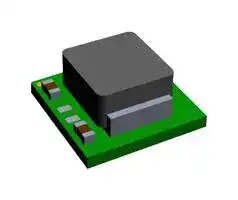
MUN12AD01-SH
Non Isolated POL DC/DC Converter, Micro Module, 5 W, 1 V, 5 V, 1 A
⚠️ Reference pricing provided. In case of supply shortages, we will connect you with our trusted procurement partners to ensure your project's continuity.
- Manufacturer: CYNTEC
- Product type: DC / DC Non Isolated Board Mount Converters - Adjustable Output
- SVHC: No SVHC (21-Jan-2025)
- Depth: 3.5mm
- Width: 3.5mm
- Height: 1.7mm
- Product Range: -
- Output Power Max: 5W
- Output Current Max: 1A
- Output Voltage Max: 5V
- Output Voltage Min: 1V
- Input Voltage DC Max: 17V
- Input Voltage DC Min: 4.5V
- DC / DC Converter Type: Micro Module
- Power Supply Applications: -
- DC / DC Converter Output Type: Adjustable
| Delivery and price | |
|---|---|
| Units per pack | 500 |
| Price | 3.02 € |
| Current stock | 500+ |
| Lead time | 30 days |
Datasheet

## **uPOL MODULE** ## **1000mA, High Efficiency uPOL Module** ## **MUN12AD01-SH** ## **FEATURES:** - High Density uPOL Module - 1000mA Output Current - 95% Peak Efficiency at 12VIN - Input Voltage Range from 4.5V to 17V - Output Voltage Range from 1.0V to 5.0V - Enable / PGOOD Function - Automatic Power Saving/PWM Mode - Protections (OCP: Non-latching, OTP) - Adjustable Soft Start Function - Compact Size: 3.5mm*3.5mm*1.7mm - Pb-free for RoHS compliant - MSL 2, 260℃ Reflow ## **APPLICATIONS:** - Point of Load Conversion - LDOs Replacement - Set Top Box / DSL Modem / AP Router - Industrial Personal Computer ## **GENERAL DESCRIPTION:** The uPOL module is non-isolated dc-dc converter that can deliver up to 1000mA of output current. The PWM switching regulator, high frequency power inductor are integrated in one hybrid package. It only needs input/output capacitors and one voltage dividing resistor to perform properly. The module has automatic operation with PWM mode and power saving mode according to loading, through constant on-time control, the module offers a simpler control loop and faster transient response. Other features include remote enable function, internal soft-start, non-latching over current protection, power good, input under voltage locked-out capability. The low profile and compact size package (3.5mm × 3.5mm x 1.7mm) is suitable for automated assembly by standard surface mount equipment. The uPOL module is Pb-free and RoHS compliance. **==> picture [466 x 290] intentionally omitted <==** **----- Start of picture text -----**<br> TYPICAL APPLICATION CIRCUIT & PACKAGE:<br>VBia s<br>EN<br>RPG VP GOOD<br>EN P GOOD<br>VIN VOUT<br>VIN Vout<br>uP OL Module<br>CFB<br>CIN SS FB COUT<br>CSS GND RFB<br>L FIGURE.1 TYPICAL APPLICATION CIRCUIT r FIGURE.2 HIGH DENSITY LOW PROFILE %<br>uPOL MODULE<br> *<br>1 Rev.A1<br>**----- End of picture text -----**<br> ## **MUN12AD01-SH** |**MUN12AD01-SH**<br>Greyntec|**MUN12AD01-SH**<br>Greyntec|**MUN12AD01-SH**<br>Greyntec|**MUN12AD01-SH**<br>Greyntec| |---|---|---|---| |**ORDER INFORMATION:**<br>~~Ld~~|||| |**Ambient Temp. Range**|**Package**||| |**Part Number**||**MSL**|**Note**| |**(°C)**|**(Pb-Free)**||| |MUN12AD01-SH<br>-40 ~ +85|DFN|Level 2|-| ||||| |**Order Code**|**Packing**||**Quantity**| |MUN12AD01-SH|Tape and reel||1000| **==> picture [461 x 14] intentionally omitted <==** **----- Start of picture text -----**<br> PIN CONFIGURATION: be<br>**----- End of picture text -----**<br> **==> picture [462 x 167] intentionally omitted <==** **----- Start of picture text -----**<br> SS (1) (8) VIN<br>LL<br>a<br>7 |} 7<br>FB (2) (7) EN<br>Lt | pL<br>(9) GND<br>ra lr<br>PGOOD (3) Lt | J Lo (6) NC<br>Ll<br>-7-7<br>VOUT (4) (5) GND<br>**----- End of picture text -----**<br> **TOP VIEW** 2 Rev.A1 ## **MUN12AD01-SH** ## **PIN DESCRIPTION:** |**Symbol**|**Pin No.**|**Description**| |---|---|---| |SS|1|Leave SS pin floating for default 1ms soft-start time. For longer than 1ms<br>soft-start time, connect a capacitor from SS to GND.<br>Tss(ms)=Css(nF)*0.6V/4uA| |FB|2|Feedback input. Connect an external resistor divider from the output to<br>GND to set the output voltage.| |PGOOD|3|Power Good indicator. The pin output is an open drain that can connect to<br>VIN byresistor.| |VOUT|4|Power output pin. Connect to output for the load.| |GND|5, 9|Power ground pin for signal, input, and output return path. This pin<br>needs to be connected to one or moregroundplane directly.| |NC|6|No connection| |EN|7|On/Off control pin for module.<br>EN = LOW, the module is off.<br>EN = HIGH, the module is on.<br>Do not float.| |VIN|8|Power input pin. It needs to be connected to input rail.| 3 Rev.A1 **MUN12AD01-SH** ## **ELECTRICAL SPECIFICATIONS:** CAUTION: Do not operate at or near absolute maximum rating listed for an extended period of time. This stress may adversely impact product reliability and result in failures outside of warranty. |**Parameter**<br>~~a~~|**Description**<br>|**Min.**<br>|**Typ.**<br>|**Max.**<br>|**Unit**<br>| |---|---|---|---|---|---| |◼<br>Absolute Maximum Ratings<br>~~ee~~|||||| |VIN to GND<br>~~ee~~<br>~~es~~|~~ee~~<br>~~ee~~|-<br>~~ee~~<br>~~ee~~|-<br>~~ee~~<br>~~ee~~|+19.0<br>~~ee~~<br>~~ee~~|V<br>~~ee~~<br>~~ee~~| |VOUT to GND<br>~~es~~<br>~~ee~~|~~ee~~|-<br>~~ee~~|-<br>~~ee~~|+6.5<br>~~ee~~|V<br>~~ee~~| |FB to GND<br>~~es~~<br>~~ee~~<br>~~es~~|~~ee~~|-<br>~~ee~~|-<br>~~ee~~|+4.0<br>~~ee~~|V<br>~~ee~~| |EN to GND<br>~~ee~~<br>~~es~~||-|-|VIN+0.3|V| |PGOOD to GND<br>~~es~~<br>~~a~~||-|-|+19.0|V| |Tc<br>~~a~~<br>~~a~~<br>~~es~~|Case Temperature of Inductor|-|-|+110|°C| |Tj<br>~~a~~<br>~~es~~<br>~~ee~~|Junction Temperature<br>~~ee~~|-40<br>~~ee~~|-<br>~~ee~~|+125<br>~~ee~~|°C<br>~~ee~~| |Tstg<br>~~es~~<br>~~ee~~|Storage Temperature<br>~~ee~~|-40<br>~~ee~~<br>~~ee~~|-<br>~~ee~~|+125<br>~~ee~~|°C<br>~~ee~~| |ESD Rating<br>~~ee~~|Human Body Model (HBM)<br>~~ee~~|-<br>~~ee~~<br>~~ee~~|-<br>~~ee~~|2k<br>~~ee~~|V<br>~~ee~~| ||Machine Model (MM)<br>~~es~~|-<br>~~ee~~<br>~~es~~<br>~~ee~~|-<br>~~es~~|200<br>~~es~~|V<br>~~es~~| ||Charge Device Model (CDM)<br>~~es~~|-<br>~~es~~<br>~~ee~~|-<br>~~es~~|500<br>~~es~~|V<br>~~es~~| |◼<br>Recommendation Operating Ratings<br>~~ee~~<br>~~a~~<br>~~ee~~|||||| |VIN<br>~~ee~~<br>~~ee~~|Input Supply Voltage|+4.5|-|+17.0|V| |VOUT<br>~~ee~~<br>~~ee~~<br>~~ee~~|Adjusted Output Voltage|+1.0|-|+5.0|V| |PGOOD<br>~~ee~~<br>~~ee~~<br>~~es~~|Power Good Voltage|-|-|+17.0|V| |Ta<br>~~ee~~<br>~~es~~|Ambient Temperature|-40|-|+85|°C| |◼<br>Thermal Information<br>~~es~~<br>~~a~~|||||| |Rth(jchoke-a)|Thermal resistance from junction to<br>ambient. (Note 1)|-|51|-|°C/W| NOTES: 1. Rth(jchoke-a) is measured with the component mounted on an effective thermal conductivity test board on 0 LFM condition. The test board size is 42mm× 42mm× 1.6mm with 4 layers, 1oz. The test condition is complied with JEDEC EIJ/JESD 51 Standards. 4 Rev.A1 **MUN12AD01-SH** ## **ELECTRICAL SPECIFICATIONS: (Cont.)** Conditions: TA = 25 ºC, unless otherwise specified. Test Board Information: 42mm× 42mm× 1.6mm, 4 layers, 1oz. The output ripple and transient response are measured by short loop probing and limited to 20MHz bandwidth. Cin = 22uF/25V/0805, Cout = 47uF/10V/1206. |~~a~~|~~ee~~|||||| |---|---|---|---|---|---|---| |**Symbol**<br>~~a~~<br>~~en~~|**Parameter**<br>~~ee~~<br>~~en~~|**Conditions**|**Min.**|**Typ.**|**Max.**|**Unit**| |◼<br>Input Characteristics<br>~~a~~<br>~~ee~~<br>~~en~~||||||| |ISD(IN)<br>~~en~~<br>~~a~~|Input shutdown<br>current<br>~~en~~|Vin =12V, EN = GND|-<br>~~es~~|5.5|-|uA| |IS(IN)<br>~~a~~<br>~~===~~|Input supply current<br>~~===~~|Vin =12V, EN = VIN<br>~~es~~<br>~~===~~|-<br>~~es~~<br>~~es~~<br>~~===~~|-<br>~~es~~<br>~~===~~|-<br>~~es~~<br>~~===~~|-<br>~~es~~<br>~~===~~| |||Iout = 0A,Vout = 3.3V<br>~~ee~~<br>~~===~~|-<br>~~es~~<br>~~ee~~<br>~~===~~|0.25<br>~~ee~~<br>~~===~~|-<br>~~ee~~<br>~~===~~|mA<br>~~ee~~<br>~~===~~| |||Iout = 1mA,Vout = 3.3V<br>~~ee~~<br>~~===~~|-<br>~~ee~~<br>~~===~~|0.6<br>~~ee~~<br>~~===~~|-<br>~~ee~~<br>~~===~~|mA<br>~~ee~~<br>~~===~~| |||Iout = 100mA, Vout = 3.3V<br>~~===~~|-<br>~~===~~|33<br>~~===~~|-<br>~~===~~|mA<br>~~===~~| |||Iout = 1000mA, Vout = 3.3V<br>~~===~~<br>~~ee~~|-<br>~~===~~<br>~~ee~~|320<br>~~===~~<br>~~ee~~|-<br>~~===~~<br>~~ee~~|mA<br>~~===~~<br>~~ee~~| |◼<br>Output Characteristics<br>~~===~~<br>~~ee~~<br>~~|~~||||||| |IOUT(DC)<br>~~ee~~|Output continuous<br>current range<br>~~ee~~|Vin=12V, Vout=3.3V<br>~~ee~~|0<br>~~ee~~|-<br>~~ee~~|1000<br>~~ee~~|mA<br>~~ee~~| |VO(SET)<br>~~ee~~|Ouput voltage set<br>point<br>~~ee~~|With 0.5% tolerance for external<br>resistor used to set output<br>voltage<br>~~ee~~|-3.0<br>~~ee~~|-<br>~~ee~~|+3.0<br>~~ee~~|% VO(SET)<br>~~ee~~| |ΔVOUT<br>/ΔVIN<br>~~ee~~|Line regulation<br>accuracy<br>~~ee ~~|Vin = 5V to 12V<br>Vout = 3.3V, Iout = 0A<br>Vout = 3.3V,Iout = 1000mA<br> ~~ee ~~|-<br> ~~ee~~|0.1<br>~~ee~~|0.2<br>~~ee~~|% VO(SET)<br>~~ee~~| |ΔVOUT<br>/ΔIOUT<br>~~a~~|Load regulation<br>accuracy|Iout = 0A to 1000mA<br>Vin = 12V,Vout = 3.3V|-<br>~~ee~~|0.5<br>~~ee~~|1.0<br>~~eee~~|% VO(SET)<br>~~eee~~| |VOUT(AC)|Output ripple voltage|Vin = 12V, Vout = 3.3V<br>EN = VIN<br>~~ee~~|-<br>~~ee~~<br>~~ee~~<br>~~es~~|-<br>~~ee~~<br>~~ee~~<br>~~ee~~|-<br>~~ee~~<br>~~eee~~<br>~~ee~~|-<br>~~ee~~<br>~~eee~~| |||Iout = 1mA<br>~~es~~|-<br>~~ee ~~<br>~~es~~<br>~~es~~<br>~~ee~~|14<br> ~~ee ~~<br>~~es~~<br>~~ee~~<br>~~ee~~|-<br> ~~eee~~<br>~~es~~<br>~~ee~~|mVp-p<br>~~eee~~<br>~~es~~| |||Iout = 1000mA<br>~~ee~~|-<br>~~es ~~<br>~~ee~~<br>~~ee~~|8<br> ~~ee ~~<br>~~ee~~<br>~~ee~~|-<br> ~~ee~~<br>~~ee~~|mVp-p<br>~~ee~~| |◼<br>Control Characteristics<br>~~ee ee~~<br>~~ee~~<br>~~es~~||||||| |VREF<br>~~es~~<br>~~a~~|Referance voltage<br>~~ee~~||0.591|0.600|0.609|V| |FOSC<br>~~es~~<br>~~a~~<br>~~a~~|Oscillator frequency<br>~~ee~~<br>~~es~~|PWM Operation|-|1.0|-|MHz| |VUVLO<br>~~a ~~<br>~~a~~<br>~~es~~|Input UVLO threshold<br> ~~ee~~<br>~~es~~<br>||-<br>|-<br>|4.5<br>|V<br>| |VPGL<br>~~a ~~<br>~~es~~|PGOOD output low<br> ~~es~~<br>|IPGOOD=4mA<br>|0.04<br>|0.15<br>|0.3<br>|V<br>| |VEN_TH<br>~~esee~~|Enable rising<br>threshold voltage<br>~~ee~~<br>~~ee~~|~~ee~~|1.5<br>~~ee~~|-<br>~~ee~~|-<br>~~ee~~|V<br>~~ee~~| ||Enable falling<br>threshold voltage<br>~~ee~~<br>~~ee~~|~~ee~~|-<br>~~ee~~|-<br>~~ee~~|0.4<br>~~ee~~|V<br>~~ee~~| |◼<br>Fault Protection<br>~~ee~~<br>~~ne~~<br>~~eees~~||||||| |TOTP<br>~~ee~~<br>~~a~~|Over temp protection<br>~~es~~<br>~~ee~~|~~es~~<br>~~ee~~|-<br>~~es~~<br>~~ee~~|150<br>~~es~~<br>~~ee~~|-<br>~~es~~<br>~~ee~~<br>~~ee~~|°C<br>~~es~~<br>~~ee~~<br>~~ee~~| |ILIMIT_TH<br>~~ee~~<br>~~a~~|Current limit<br>threshold<br>~~es~~<br>~~ee~~|Peak value of inductor current<br>~~es~~<br>~~ee~~|1.3<br>~~es~~<br>~~ee~~|-<br>~~es~~<br>~~ee~~|2.3<br>~~es~~<br>~~ee~~<br>~~ee~~|A<br>~~es~~<br>~~ee~~<br>~~ee~~| 5 Rev.A1 **MUN12AD01-SH** ## **TYPICAL PERFORMANCE CHARACTERISTICS: (1.0VOUT)** Conditions: TA = 25 ºC, unless otherwise specified. Test Board Information: 42mm× 42mm× 1.6mm, 4 layers, 1oz. The output ripple and transient response are measured by short loop probing and limited to 20MegHz bandwidth. Cin = 22uF/25V/0805, Cout = 47uF/10V/1206. The following figures are the typical characteristic curves at 1.0Vout. **==> picture [403 x 378] intentionally omitted <==** **----- Start of picture text -----**<br> FIG.3 EFFICIENCY V.S. LOAD CURRENT FIG.4 DE-RATING CURVE AT 12VIN<br>cee eee: | TekFrevu a ee | ees|<br>VOUT VOUT<br>25,0kS/s T ; 1,2568/s f<br>Lok points 7.20 (Doomey Si>v0.000000s__t0kpoints_—_ 4.609<br>Value10.0mv Mean10.9m Min4.30m Max12.0m Std Dev139m @ Peak—Peak Value5,20mV¥ Mean5.58m Min4.40m Max7.60m Std Dey668<br>FIG.5 OUTPUT RIPPLE FIG.6 OUTPUT RIPPLE<br>(12VIN, IOUT=0A) (12VIN, IOUT=1A)<br>Gees aes Ann Tek Stop Es Se oes<br>VOUT VOUT<br>PGOOD<br>IOUT<br>EN<br>TOs 10.0MS/s 7 sd meine Sevens<br>WD Sms Ur 240.0000 _tokpoits 810m<br>Value Mean Min Max Std Dev<br>= 23.6mV ——24.4m 2.4m 25.6m 1.03m @ tov & 1.00ms 1.00MS/s f<br>-10.0m¥—_-10.8m13.6mV 13.6m -12.4m12.0m -8.80m14.8m 859y980y 5.00V U>¥4.000000ps 10k points 2.00V<br>FIG.7 TRANSIENT RESPONSE FIG.8 TURN-ON<br>(12VIN, 50% to 100% LOAD STEP) (12VIN, IOUT=1A)<br>**----- End of picture text -----**<br> 6 Rev.A1 **MUN12AD01-SH** ## **TYPICAL PERFORMANCE CHARACTERISTICS: (1.8VOUT)** Conditions: TA = 25 ºC, unless otherwise specified. Test Board Information: 42mm× 42mm× 1.6mm, 4 layers, 1oz. The output ripple and transient response are measured by short loop probing and limited to 20MegHz bandwidth. Cin = 22uF/25V/0805, Cout = 47uF/10V/1206. The following figures are the typical characteristic curves at 1.8Vout. **==> picture [410 x 378] intentionally omitted <==** **----- Start of picture text -----**<br> FIG.9 EFFICIENCY V.S. LOAD CURRENT FIG.10 DE-RATING CURVE AT 12VIN<br>A Gennes eee Ae TekPrevu (eeA<br>VOUT VOUT<br>25.0kS/s [i wa ; 1,2568/s f<br>1k points__2.40mV G¥240,0000ys _1Okpoints___5.40V<br>Value14.0mV Mean14.6m Min13.6m Max16.0m Std Dev602p @ Peak-Peak Value5.60mv Mean6.20m Min4.80m Max10.4m Std939p Dev<br>FIG.11 OUTPUT RIPPLE FIG.12 OUTPUT RIPPLE<br>(12VIN, IOUT=0A) (12VIN, IOUT=1A)<br>ee a: Ai Tek Stop A eee:eee An<br>VOUT VOUT<br>IOUT Aa Leemnnenrnrananennne PGOOD<br>< aad<br>EN<br>a _ (f00ps 10.0MS/s 7 sd = :<br>U+¥240,0000is__10kpoints__810mA :<br>Value Mean Min Max Std Dev<br>18.2mV 178m 17.4m 18.2m 566) 5.00¥ G>¥4.000000ys 10k points 2.00<br>-14.6mV -14.6m -14.6m -14.6m 0,00<br>FIG.13 TRANSIENT RESPONSE FIG.14 TURN-ON<br>(12VIN, 50% to 100% LOAD STEP) (12VIN, IOUT=1A)<br>**----- End of picture text -----**<br> 7 Rev.A1 **MUN12AD01-SH** ## **TYPICAL PERFORMANCE CHARACTERISTICS: (3.3VOUT)** Conditions: TA = 25 ºC, unless otherwise specified. Test Board Information: 42mm× 42mm× 1.6mm, 4 layers, 1oz. The output ripple and transient response are measured by short loop probing and limited to 20MegHz bandwidth. Cin = 22uF/25V/0805, Cout = 47uF/10V/1206. The following figures are the typical characteristic curves at 3.3Vout. **==> picture [424 x 390] intentionally omitted <==** **----- Start of picture text -----**<br> FIG.15 EFFICIENCY V.S. LOAD CURRENT FIG.16 DE-RATING CURVE AT 12VIN<br>| 7 kee _ —s————rTTT—Sd<br>VOUT VOUT<br>— coe ceecnee<br>(@DSit0.0my ve 20.0ms¥240.0000ys 50.0kS/s0k points [i7.20miwa (@DSGt0.0my vy 800ns 240.0000ps 1,2568/s—10kpoints [35.40Wi<br>PD Peak—Peak 4 Om 3.9m 4 0m 4m Sm PD Peak—Peak 680m 680m 680m 680m 0,00<br>FIG.17 OUTPUT RIPPLE FIG.18 OUTPUT RIPPLE<br>(12VIN, IOUT=0A) (12VIN, IOUT=1A)<br>stop EE<br>VOUT<br>VOUT<br>tf a<br>IOUT PGOOD<br>EN<br>(@D 20.0 GD] S004 ¥240.0000us 10k points 810A Dip ithe . :<br>@ [Peak-Peak] 53.6mVValue 54.2mMean Min52.0m Max56.0m Std1.41m Dev<br>@ max 27,.6mV 28.8m 27,.6m 30.0m 714y 5<br>FIG.19 TRANSIENT RESPONSE FIG.20 TURN-ON<br>(12VIN, 50% to 100% LOAD STEP) (12VIN, IOUT=1A)<br>**----- End of picture text -----**<br> 8 Rev.A1 **MUN12AD01-SH** ## **TYPICAL PERFORMANCE CHARACTERISTICS: (5.0VOUT)** Conditions: TA = 25 ºC, unless otherwise specified. Test Board Information: 42mm× 42mm× 1.6mm, 4 layers, 1oz. The output ripple and transient response are measured by short loop probing and limited to 20MegHz bandwidth. Cin = 22uF/25V/0805, Cout = 47uF/10V/1206. The following figures are the typical characteristic curves at 5.0Vout. **==> picture [412 x 379] intentionally omitted <==** **----- Start of picture text -----**<br> FIG.21 EFFICIENCY V.S. LOAD CURRENT FIG.22 DE-RATING CURVE AT 12VIN<br>A eens eeeeeeeeeeeecces A Tek Prevu<br>VOUT VOUT<br>Sn eh, er, aml ft<br>| ; | | | ; face<br>SGve Value 10.0ms240.0000) 100kS/s10k points 1.60f (@D 10.00 vy JG240.0000ys800ns 1,2568/s_t0kpoints 5.40f<br>32.0mV 40.9mMean 29.6mMin Max46.4m 4,03mStd Dev @ Peak-Peak Value11.2mV Mean11.3m Min10.8m Max12.0m Std Dey393<br>FIG.23 OUTPUT RIPPLE FIG.24 OUTPUT RIPPLE<br>(12VIN, IOUT=0A) (12VIN, IOUT=1A)<br>Ee Gee es Ae Tek Stop A<br>VOUT VOUT<br>PGOOD<br>IOUT<br>: L i A<br>EN<br>Ve GBD S00 240.100ys 0000p 10 k.0MS/s points __—_810mAf<br>Value Mean Min Max Std Dev ,<br>42.0mV 42.1m 40.4m 43.6m 728) - -<br>=33.8mV =39.4m =41.2m =38.8m 80<br>FIG.25 TRANSIENT RESPONSE FIG.26 TURN-ON<br>(12VIN, 50% to 100% LOAD STEP) (12VIN, IOUT=1A)<br>**----- End of picture text -----**<br> 9 Rev.A1 **MUN12AD01-SH** ## **APPLICATIONS INFORMATION:** ## **REFERENCE CIRCUIT FOR GENERAL APPLICATION:** **==> picture [448 x 295] intentionally omitted <==** **----- Start of picture text -----**<br> Figure 27 shows the module application schematics for input voltage +12V and turn on by input<br>voltage directly through enable resistor (REN).<br>VBia s<br>EN RPG<br>100k/0402 VP GOOD<br>Enable/Disable control<br>EN P GOOD<br>VIN VOUT<br>VIN Vout<br>u P OL Module CFB<br>100 pF/10 V/0201<br>CIN SS FB COUT<br>22uF /25V/0805 CSS GND S e tting RFB 47 uF/10 V/1206<br>DNP/0402 Output Volta ge<br>+L<br>FIG.27 REFERENCE CIRCUIT FOR GENERAL APPLICATION<br>**----- End of picture text -----**<br> 10 Rev.A1 **MUN12AD01-SH** ## **APPLICATIONS INFORMATION: (Cont.)** ## **RECOMMENDATION LAYOUT GUIDE:** In order to achieve stable, low losses, less noise or spike, and good thermal performance some layout considerations are necessary. The recommendation layout is shown as Figure 28. 1. The ground connection between pin 5 and 9 should be a solid ground plane under the module. It can be connected one or more ground plane by using several Vias. 2. Place high frequency ceramic capacitors between pin 4 (VOUT), and pin 5, 9 (GND) for output side, as close to module as possible to minimize high frequency noise. 3. Keep the RFB and CFB connection trace to the module pin 2 (FB) short. 4. Use large copper area for power path (VIN, VOUT, and GND) to minimize the conduction loss and enhance heat transferring. Also, use multiple Vias to connect power planes in different layer. **FIG.28 RECOMMENDATION LAYOUT** 11 Rev.A1 **MUN12AD01-SH** ## **APPLICATIONS INFORMATION: (Cont.)** ## **SAFETY CONSIDERATIONS:** Certain applications and/or safety agencies may require fuses at the inputs of power conversion components. Fuses should also be used when there is the possibility of sustained input voltage reversal which is not current limited. For greatest safety, we recommend a fast blow fuse installed in the ungrounded input supply line. The installer must observe all relevant safety standards and regulations. For safety agency approvals, install the converter in compliance with the end-user safety standard. ## **INPUT FILTERING:** The module should be connected to a source supply of low AC impedance and high inductance in which line inductance can affect the module stability. An input capacitor must be placed as near as possible to the input pin of the module so to minimize input ripple voltage and ensure module stability. ## **OUTPUT FILTERING:** To reduce output ripple and improve the dynamic response as the step load changes, an additional capacitor at the output must be connected. Low ESR polymer and ceramic capacitors are recommended to improve the output ripple and dynamic response of the module. ## **PROGRAMMING OUTPUT VOLTAGE:** The module has an internal 0.6V ± 2% reference voltage. The output voltage can be programmed by the dividing resistor (RFB) which connects to both FB pin and GND pin. The output voltage can be calculated by Equation 1, resistor choice may be referred to TABLE 1. **==> picture [309 x 38] intentionally omitted <==** |VOUT (V)|RFB(k)| |---|---| |1.0|150(1%)| |1.2|100(1%)| |1.8|50(1%)| |2.5|31.6(1%)| |3.3|22.1(1%)| **TABLE 1 Resistor values for common output voltages** 12 Rev.A1 **MUN12AD01-SH** ## **APPLICATIONS INFORMATION: (Cont.)** ## **Thermal Considerations:** All of thermal testing condition is complied with JEDEC EIJ/JESD 51 Standards. Therefore, the test board size is 42mm× 42mm× 1.6mm with 4 layers 1oz. The case temperature of module sensing point is shown as Figure 29. Then Rth(jchoke-a) is measured with the component mounted on an effective thermal conductivity test board on 0 LFM condition. The MUN12AD01-SH power module is designed for using when the case temperature is below 110°C regardless the change of output current, input/output voltage or ambient temperature. **Sensing Point (Defined case temperature)** **Figure 29. Case Temperature Sensing Point** 13 Rev.A1 **MUN12AD01-SH** ## **REFLOW PARAMETERS:** Lead-free soldering process is a standard of electronic products production. Solder alloys like Sn/Ag, Sn/Ag/Cu and Sn/Ag/Bi are used extensively to replace the traditional Sn/Pb alloy. Sn/Ag/Cu alloy (SAC) is recommended for this power module process. In the SAC alloy series, SAC305 is a very popular solder alloy containing 3% Ag and 0.5% Cu and easy to obtain. Figure 30 shows an example of the reflow profile diagram. Typically, the profile has three stages. During the initial stage from room temperature to 150°C, the ramp rate of temperature should not be more than 3°C/sec. The soak zone then occurs from 150°C to 200°C and should last for 60 to 120 seconds. Finally, keep at over 217°C for 60~150 seconds to melt the solder and make the peak temperature at the range from 255°C to 260°C (Do not exceed 30 sec). It is noted that the time of peak temperature should depend on the mass of the PCB board. The reflow profile is usually supported by the solder vendor and one should adopt it for optimization according to various solder type and various manufacturers’ formulae. **FIG.30 Recommendation Reflow Profile** ## **(Not to scale)** ## ***Refer to the Classification Reflow Profile of J-STD-020.** 14 Rev.A1 **MUN12AD01-SH** > **PACKAGE OUTLINE DRAWING:** ~~Ld~~ ## Unit: mm 15 Rev.A1 **MUN12AD01-SH** ## **LAND PATTERN REFERENCE:** DC Unit: mm 1.60 a ; ——+—+ BaP LAP et 1.90 5 RECOMMENDED LAND PATTERN C0.25 1.60 0.75 1 7 8 FE ee aoei —_+— — —— in — —+ poh || | Be RECOMMENDED STENCIL PATTERN* *Based on 0.1~0.15mm thickness stencil (Reference only) *Recommended solder paste coverage 55~100% 16 Rev.A1 **MUN12AD01-SH** ## **PACKING REFERENCE:** **==> picture [353 x 264] intentionally omitted <==** **----- Start of picture text -----**<br> Unit: mm<br>Package In Tape Loading Orientation<br>PIN 4 Sprocket<br>Bn<br>3.50 8<br>g<br>Tape Dimension<br>**----- End of picture text -----**<br> 17 Rev.A1 **MUN12AD01-SH** ## **PACKING REFERENCE: (Cont.)** **==> picture [353 x 184] intentionally omitted <==** **----- Start of picture text -----**<br> Unit: mm<br>Reel Dimension<br>See Detail A ==<br>\<br>| _ | |<br>| -)<br>Detail A<br>Ge =<br>**----- End of picture text -----**<br> ## **Peel Strength of Top Cover Tape** The peel speed shall be about 300mm/min. The peel force of top cover tape shall be between 0.1N to 1.3N 18 Rev.A1 **MUN12AD01-SH** ## **REVISION HISTORY:** |~~es es~~|~~es~~|| |---|---|---| |**Date**<br>~~es es~~<br>~~ee~~|**Revision**<br>~~es~~<br>~~es~~|**Changes**| |2014.06.24<br>~~es es~~<br>~~ee~~<br>~~ee~~|00<br>~~es~~<br>~~es~~<br>~~es~~|Release the preliminary specification.| |2014.07.09<br>~~ee~~<br>~~ee~~<br>~~ee es~~|01<br>~~es~~<br>~~es~~<br>~~es~~|Update application and POD drawing.| |2014.09.17<br>~~ee~~<br>~~ee es~~<br>~~ee es~~|02<br>~~es~~<br>~~es~~<br>~~es~~|Update Electrical specifications and packing information.| |2014.11.24<br>~~ee es~~<br>~~ee es~~<br>~~ee es~~|03<br>~~es~~<br>~~es~~<br>~~es~~|Adjust Fig. sequence.| |2014.12.11<br>~~ee es~~<br>~~ee es~~<br>~~ee~~|04<br>~~es~~<br>~~es~~<br>~~es~~|Update land pattern reference.| |2014.12.31<br>~~ee es~~<br>~~ee~~<br>~~es~~|05<br>~~es~~<br>~~es~~|Update uPOL module to LDS module.| |2015.02.26<br>~~ee~~<br>~~es~~|06<br>~~es~~|Update POD and PIN 1 drawing.| |2015.06.05<br>~~es~~<br>~~ee~~|07<br>~~es~~|Update recommendation layout and schematic<br>Change pin 6 define to N.C.| |2015.06.24<br>~~ee~~<br>~~ee es~~|08<br>~~es~~<br>~~es~~|Add REFLOW PARAMETERS| |2015.09.01<br>~~ee~~<br>~~ee es~~<br>~~ee~~|09<br>~~es~~<br>~~es~~<br>~~es~~|Add constant on-time control in general description.| |2015.11.17<br>~~ee es~~<br>~~ee~~<br>~~ee~~|10<br>~~es~~<br>~~es~~<br>~~es~~|Change recommendation reflow profile| |2016.01.25<br>~~ee ~~<br>~~ee~~<br>~~ee~~|11<br> ~~es~~<br>~~es~~<br>~~es~~|Modify outline drawing.| |2016.06.28<br>~~ee ~~<br>~~ee~~<br>~~ee~~|12<br> ~~es~~<br>~~es~~<br>~~es~~|Modify land pattern reference| |2017.07.03<br>~~ee ~~<br>~~ee~~|13<br> ~~es~~<br>~~es~~|Add PGOOD sink current spec| |2022.12.20<br>~~ee ~~<br>~~ee~~|14<br> ~~es~~|1. Page 13, add test board information”1oz”.<br>2. Page 14, update reflow parameters and FIG.30.<br>3. Page 16, change the thickness description of stencil. Add note<br>and unit.| |2024.12.16<br>~~ee~~|A1|Synchronized with document management number| 19 Rev.A1
Updated at June 9, 2026
About Novapart
Novapart is a B2B electronic component broker specialising in stock shortages and cost reduction. We source hard-to-find parts and identify compliant alternatives across a catalogue of 410,000+ components from 500+ manufacturers.
Learn more →Stock Shortage Specialist
When a component is unavailable, discontinued or has an unacceptable lead time, we tap into our network of vetted European and Asian distributors to source what you need — without compromising on quality or traceability.
Request a quote →Compliant Alternatives
We identify pin-to-pin, electrically equivalent substitutes that meet the same certifications (RoHS, AEC-Q100, REACH) as your original specification — validated against datasheets, not just part numbers. Often at a lower cost.
BOM Analysis service →