
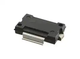


MRFE6VS25GNR1
RF FET Transistor, 133 VDC, 1.8 MHz, 2000 MHz, TO-270
- Manufacturer: NXP
- Product type: RF FETs
- Drain Source Voltage Vds:133VDC; Continuous Drain Current Id:-; Power Dissipation Pd:-; Operating Frequency Min:1.8MHz; Operating Frequency Max:2000MHz; RF Transistor Case:TO-270; No. of P
- MSL: MSL 3 - 168 hours
- SVHC: No SVHC (27-Jun-2024)
- No. of Pins: 2Pins
- Channel Type: N Channel
- Product Range: -
- Power Dissipation: -
- Transistor Mounting: Flange
- Transistor Case Style: TO-270
- Operating Frequency Max: 2000MHz
- Operating Frequency Min: 1.8MHz
- Drain Source Voltage Vds: 133VDC
- Operating Temperature Max: 225°C
- Continuous Drain Current Id: -
| Delivery and price | |
|---|---|
| Units per pack | 500 |
| Price | 24.18 € |
| Current stock | 10+ |
| Lead time | 30 days |
**Freescale Semiconductor** Technical Data
Document Number: MRFE6VS25N Rev. 1, 12/2012
## **RF Power LDMOS Transistors**
## High Ruggedness N--Channel Enhancement--Mode Lateral MOSFETs
RF power transistors designed for both narrowband and broadband ISM, broadcast and aerospace applications operating at frequencies from 1.8 to 2000 MHz. These devices are fabricated using Freescale’s enhanced ruggedness platform and are suitable for use in applications where high VSWRs are encountered.
## **Typical Performance:** VDD = 50 Volts
|**Frequency**<br>**(MHz)**|**Signal Type**|**Pout**<br>**(W)**|**Gps**<br>**(dB)**|**D**<br>**(%)**|**IMD (1)**<br>**(dBc)**|
|---|---|---|---|---|---|
|1.8 to 30 **(2,6)**|Two--Tone<br>(10 kHz spacing)|25 PEP|25|51|--30|
|30--512 **(3,6)**|Two--Tone<br>(200 kHz spacing)|25 PEP|17.1|30.1|--32|
|512 **(4)**|Pulse (100sec,<br>20% Duty Cycle)|25 Peak|25.4|74.5|—|
|512 **(4)**|CW|25|25.5|74.7|—|
|1030 **(5)**|CW|25|22.5|60|—|
## **Load Mismatch/Ruggedness**
|**Frequency**<br>**(MHz)**|**Signal Type**|**VSWR**|**Pin**<br>**(W)**|**Test**<br>**Voltage**|**Result**|
|---|---|---|---|---|---|
|30 **(2)**|CW|>65:1<br>at all Phase<br>Angles|0.23<br>(3 dB<br>Overdrive)|50|No Device<br>Degradation|
|512 **(3)**|CW||1.6<br>(3 dB<br>Overdrive)|||
|512 **(4)**|Pulse<br>(100sec, 20%<br>Duty Cycle)||0.14 Peak<br>(3 dB<br>Overdrive)|||
|512 **(4)**|CW||0.14<br>(3 dB<br>Overdrive|||
|1030 **(5)**|CW||0.34<br>(3 dB<br>Overdrive|||
1. Distortion products are referenced to one of two tones. See p. 13, 20.
**MRFE6VS25NR1 MRFE6VS25GNR1** — **1.8--2000 MHz, 25 W, 50 V WIDEBAND RF POWER LDMOS TRANSISTORS**
**==> picture [70 x 110] intentionally omitted <==**
**----- Start of picture text -----**<br>
TO--270--2<br>PLASTIC<br>MRFE6VS25NR1<br>TO--270--2 GULL<br>PLASTIC<br>MRFE6VS25GNR1<br>**----- End of picture text -----**<br>
**==> picture [156 x 109] intentionally omitted <==**
**----- Start of picture text -----**<br>
Gate 1 2 Drain<br>(Top View)<br>Note: The backside of the package is the<br>source terminal for the transistor.<br>Figure 1. Pin Connections<br>**----- End of picture text -----**<br>
2. Measured in 1.8--30 MHz broadband reference circuit.
3. Measured in 30--512 MHz broadband reference circuit.
4. Measured in 512 MHz narrowband test circuit.
5. Measured in 1030 MHz narrowband test circuit.
6. The values shown are the minimum measured performance numbers across the indicated frequency range.
## **Features**
- Wide Operating Frequency Range
- Extreme Ruggedness
- Unmatched, Capable of Very Broadband Operation
- Integrated Stability Enhancements
- Low Thermal Resistance
- Extended ESD Protection Circuit
- In Tape and Reel. R1 Suffix = 500 Units, 24 mm Tape Width, 13--inch Reel.
**MRFE6VS25NR1 MRFE6VS25GNR1** ~~*treescale~~
Freescale Semiconductor, Inc., 2012. All rights reserved.
RF Device Data Freescale Semiconductor, Inc.
1
**Table 1. Maximum Ratings**
|**Rating**<br>**Symbol**<br>**Value**<br>**Unit**<br>Drain--Source Voltage<br>VDSS<br>--0.5, +133<br>Vdc<br>Gate--Source Voltage<br>VGS<br>--6.0, +10<br>Vdc<br>Storage Temperature Range<br>Tstg<br>--65 to +150<br>C<br>Case Operating Temperature<br>TC<br>--40 to +150<br>C<br>Operating Junction Temperature **(1,2)**<br>TJ<br>--40 to +225<br>C<br>~~=~~|
|---|
|**Table 2. Thermal Characteristics**|
|**Characteristic**<br>**Symbol**<br>**Value (2,3)**<br>**Unit**<br>Thermal Resistance, Junction to Case<br>CW: Case Temperature 80C, 25 W CW, 50 Vdc, IDQ= 10 mA, 512 MHz<br>RJC<br>1.2<br>C/W<br>Thermal Impedance, Junction to Case<br>Pulse: Case Temperature 77C, 25 W Peak, 100sec Pulse Width,<br>20% Duty Cycle, 50 Vdc, IDQ= 10 mA, 512 MHz<br>ZJC<br>0.29<br>C/W<br>~~eee~~|
|**Table 3. ESD Protection Characteristics**|
|**Test Methodology**<br>**Class**<br>Human Body Model (per JESD22--A114)<br>2, passes 2500 V<br>Machine Model (per EIA/JESD22--A115)<br>B, passes 250 V<br>Charge Device Model (per JESD22--C101)<br>IV, passes 2000 V<br>**Table 4. Moisture Sensitivity Level**<br>**Test Methodology**<br>**Rating**<br>**Package Peak Temperature**<br>**Unit**<br>Per JESD22--A113, IPC/JEDEC J--STD--020<br>3<br>260<br>C<br>~~a~~|
|**Table 5. Electrical Characteristics** (TA= 25C unless otherwise noted)|
|**Characteristic**<br>**Symbol**<br>**Min**<br>**Typ**<br>**Max**<br>**Unit**|
|**Off Characteristics**|
|Gate--Source Leakage Current<br>(VGS= 5 Vdc, VDS= 0 Vdc)<br>IGSS<br>—<br>—<br>400<br>nAdc<br>Drain--Source Breakdown Voltage<br>(VGS= 0 Vdc, ID= 50 mA)<br>V(BR)DSS<br>133<br>142<br>—<br>Vdc<br>Zero Gate Voltage Drain Leakage Current<br>(VDS= 50 Vdc, VGS= 0 Vdc)<br>IDSS<br>—<br>—<br>2<br>Adc<br>Zero Gate Voltage Drain Leakage Current<br>(VDS= 100 Vdc, VGS= 0 Vdc)<br>IDSS<br>—<br>—<br>7<br>Adc<br>**On Characteristics**<br>Gate Threshold Voltage<br>(VDS= 10 Vdc, ID= 85Adc)<br>VGS(th)<br>1.5<br>2.0<br>2.5<br>Vdc<br>Gate Quiescent Voltage<br>(VDD= 50 Vdc, ID= 10 mAdc, Measured in Functional Test)<br>VGS(Q)<br>2.0<br>2.4<br>3.0<br>Vdc<br>Drain--Source On--Voltage<br>(VGS= 10 Vdc, ID= 210 mAdc)<br>VDS(on)<br>—<br>0.28<br>—<br>Vdc<br>**Dynamic Characteristics**<br>Reverse Transfer Capacitance<br>(VDS= 50 Vdc30 mV(rms)ac @ 1 MHz, VGS= 0 Vdc)<br>Crss<br>—<br>0.26<br>—<br>pF<br>Output Capacitance<br>(VDS= 50 Vdc30 mV(rms)ac @ 1 MHz, VGS= 0 Vdc)<br>Coss<br>—<br>14.2<br>—<br>pF<br>Input Capacitance<br>(VDS= 50 Vdc, VGS= 0 Vdc30 mV(rms)ac @ 1 MHz)<br>Ciss<br>—<br>39.2<br>—<br>pF<br>1. Continuous use at maximum temperature will affect MTTF.<br>2. MTTF calculator available athttp://www.freescale.com/rf<br>.Select Software & Tools/Development Tools/Calculators to access MTTF<br>calculators by product.<br>3. Refer to AN1955,_Thermal Measurement Methodology of RF Power Amplifiers._Go tohttp://www.freescale.com/rf<br>.Select<br>~~SSSEEEE~~<br>~~—— ee~~<br>~~— ee~~|
|Documentation/Application Notes -- AN1955.|
(continued)
**MRFE6VS25NR1 MRFE6VS25GNR1**
RF Device Data Freescale Semiconductor, Inc.
2
## **Table 5. Electrical Characteristics** (TA = 25C unless otherwise noted) **(continued)**
|**Characteristic**|||**Symbol**||**Min**|**Typ**||**Max**|**Unit**|
|---|---|---|---|---|---|---|---|---|---|
|**Functional Tests (1)** (In Freescale Test Fixture, 50 ohm system) V||(In Freescale Test Fixture, 50 ohm system) VDD= 50 Vdc, I|= 50 Vdc, IDQ= 10 mA, P|= 10 mA, Pout= 25 W Peak (5 W Avg.), f = 512 MHz,||||||
|100sec Pulse Width, 20% Duty Cycle||||||||||
|Power Gain<br>Gps<br>24.0<br>25.4<br>27.0<br>dB<br>Drain Efficiency<br>D<br>70.0<br>74.5<br>—<br>%<br>Input Return Loss<br>IRL<br>—<br>--16<br>--10<br>dB<br>**Load Mismatch/Ruggedness**(In Freescale Test Fixture, 50 ohm system) IDQ= 10 mA<br>~~———~~<br>~~ee~~||||||||||
|**Frequency**<br>**Signal**|||**Pin**|||||||
|**(MHz)**<br>**Type**||**VSWR**|**(W)**||**Test Voltage, VDD**|||**Result**||
|512<br>Pulse||>65:1|0.14 Peak||50|||No Device Degradation||
|(100sec, 20% Duty Cycle)||at all Phase Angles|(3 dB Overdrive)|||||||
|CW|||0.14|||||||
||||(3 dB Overdrive)|||||||
1. Measurements made with device in straight lead configuration before any lead forming operation is applied. Lead forming is used for gull wing (GN) parts.
**MRFE6VS25NR1 MRFE6VS25GNR1**
RF Device Data Freescale Semiconductor, Inc.
3
## **TYPICAL CHARACTERISTICS**
**==> picture [235 x 176] intentionally omitted <==**
**----- Start of picture text -----**<br>
100<br>Ciss<br>S ee—— ee S | Coss<br>10 2 SS<br>SE [ ——————] [———e]<br>1 POD TID<br>PN ] Crss<br>SS SSS<br>Measured with 30 mV(rms)ac @ 1 MHz<br>VGS = 0 Vdc<br>0.1 PF |<br>0 10 20 30 40 50 60<br>VDS, DRAIN--SOURCE VOLTAGE (VOLTS)<br>C, CAPACITANCE (pF)<br>**----- End of picture text -----**<br>
**Figure 2. Capacitance versus Drain--Source Voltage**
**==> picture [243 x 175] intentionally omitted <==**
**----- Start of picture text -----**<br>
1.06<br>IDQ = 10 mA VDD = 50 Vdc<br>1.04 PN<br>1.02 Nee<br>SiSS<br>1<br>100 mA<br>0.98 Po) te<br>Ssw 150 mA<br>0.96 Pp} oP dEUS<br>50 mA<br>0.94 ee<br>--40 --20 0 20 40 60 80 100<br>TC, CASE TEMPERATURE (C)<br>GS(Q)<br>NORMALIZED V<br>**----- End of picture text -----**<br>
**Figure 3. Normalized VGS and Quiescent Current versus Case Temperature**
|**IDQ (mA)**|**Slope (mV/****C)**|
|---|---|
|10|--2.160|
|50|--1.790|
|100|--1.760|
|150|--1.680|
**==> picture [239 x 202] intentionally omitted <==**
**----- Start of picture text -----**<br>
10 [8]<br>ID = 0.6 Amps VDD = 50 Vdc<br>fsNe<br>10 [7]<br>S\SNSSS eee<br>pS<br>10 [6] 0.7 Amps<br>PoRSS<br>0.9 Amps<br>po REE<br>10 [5]<br>Ser<br>a<br>10 [4] Pt ttt ttt L_ LT | | tt ef<br>90 110 130 150 170 190 210 230 250<br>TJ, JUNCTION TEMPERATURE (C)<br>Note: MTTF value represents the total cumulative operating time<br>under indicated test conditions.<br>MTTF (HOURS)<br>**----- End of picture text -----**<br>
**Figure 4. MTTF versus Junction Temperature -- CW**
**MRFE6VS25NR1 MRFE6VS25GNR1**
RF Device Data Freescale Semiconductor, Inc.
4
**512 MHz NARROWBAND PRODUCTION TEST FIXTURE**
**==> picture [460 x 179] intentionally omitted <==**
**----- Start of picture text -----**<br>
C1<br>D°, | loo Doooooeee,° £ D of. gasFf qoooo o oeccc000©°<br>B2<br>5) C13 [C14]<br>° o) Le a s; Ld B1 °ae > @ e° oS °°<br>3 [ ° ° = °<br>O 0D0T0 0000000 ° ° — 000000 0000<br>® C2 C3 O R° C4 | leb 0° L3 °° C15 ®<br>oo00\l0000000000000 C5* °° L1 q+ [e)°[ooo eKene) ooo00d° Ale L2 LE°b C12 oc00000000000000<br>— = a<br>©00000000000LETS C6 O000000\0KeeCPSCA2 o C8 8566 y o000HY ooo000”gs(J=S° 3eso|°° |fdeocooc00df00000io)6 C10* C11 J<br>® C7 C9* 0 ° ° ° ®<br>° °<br>~~ ® Q Q ° 8<br>>wof reescale~‘semiconductor a MRFE6VS25N Oo00000 ) °<br>Rev. 1<br>CUT OUT AREA<br>**----- End of picture text -----**<br>
*C5, C9 and C10 are mounted vertically.
**Figure 5. MRFE6VS25NR1 Narrowband Test Circuit Component Layout — 512 MHz**
**Table 6. MRFE6VS25NR1 Narrowband Test Circuit Component Designations and Values — 512 MHz**
|**Part**|**Description**|**Part Number**|**Manufacturer**|
|---|---|---|---|
|B1, B2<br>Long Ferrite Beads|Long Ferrite Beads<br>2743021447|2743021447|Fair-Rite|
|C1<br>22|22F, 35 V Tantalum Capacitor<br>T491X226K035AT|T491X226K035AT|Kemet|
|C2, C13<br>0.1|0.1F Chip Capacitors<br>CDR33BX104AKWY|CDR33BX104AKWY|AVX|
|C3, C14<br>0.01|0.01F Chip Capacitors<br>C0805C103K5RAC|C0805C103K5RAC|Kemet|
|C4, C11, C12<br>180 pF Chip Capacitors|180 pF Chip Capacitors<br>ATC100B181JT300XT|ATC100B181JT300XT|ATC|
|C5<br>18 pF Chip Capacitor|18 pF Chip Capacitor<br>ATC100B180JT500XT|ATC100B180JT500XT|ATC|
|C6<br>2.7 pF Chip Capacitor|2.7 pF Chip Capacitor<br>ATC100B2R7BT500XT|ATC100B2R7BT500XT|ATC|
|C7<br>15 pF Chip Capacitor|15 pF Chip Capacitor<br>ATC100B150JT500XT|ATC100B150JT500XT|ATC|
|C8<br>36 pF Chip Capacitor|36 pF Chip Capacitor<br>ATC100B360JT500XT|ATC100B360JT500XT|ATC|
|C9<br>4.3 pF Chip Capacitor|4.3 pF Chip Capacitor<br>ATC100B4R3CT500XT|ATC100B4R3CT500XT|ATC|
|C10<br>13 pF Chip Capacitor|13 pF Chip Capacitor<br>ATC100B130JT500XT|ATC100B130JT500XT|ATC|
|C15<br>470|470F, 63 V Electrolytic Capacitor<br>MCGPR63V477M13X26-RH|MCGPR63V477M13X26-RH|Multicomp|
|L1<br>33 nH Inductor|33 nH Inductor<br>1812SMS-33NJLC|1812SMS-33NJLC|Coilcraft|
|L2<br>12.5 nH Inductor|12.5 nH Inductor<br>A04TJLC|A04TJLC|Coilcraft|
|L3<br>82 nH Inductor|82 nH Inductor<br>1812SMS-82NJLC|1812SMS-82NJLC|Coilcraft|
|PCB<br>0.030|0.030,r= 2.55<br>AD255A|AD255A|Arlon|
**MRFE6VS25NR1 MRFE6VS25GNR1**
RF Device Data Freescale Semiconductor, Inc.
5
**==> picture [476 x 235] intentionally omitted <==**
**----- Start of picture text -----**<br>
L3 B2<br>VSUPPLY<br>B1 +<br>VBIAS C12 C13 C14 C15<br>+<br>C1 C2 C3 C4<br>L2<br>L1 RF<br>OUTPUT<br>Z11 Z12 Z13 Z14 Z15 Z16 Z17 Z18 Z19<br>RF<br>INPUT Z1 Z2 Z3 Z4 Z5 Z6 Z7 Z8 Z9 Z10 C11<br>C9 C10<br>C5<br>DUT<br>C6 C7 C8<br>ae eee<br>Figure 6. MRFE6VS25NR1 Narrowband Test Circuit Schematic — 512 MHz<br>Table 7. MRFE6VS25NR1 Narrowband Test Circuit Microstrips — 512 MHz<br>**----- End of picture text -----**<br>
|**Microstrip**|**Description**||**Microstrip**||**Description**|
|---|---|---|---|---|---|
|Z1|0.2350.082Microstrip||Z11||0.4750.270Microstrip|
|Z2|0.0420.082Microstrip||Z12||0.0910.082Microstrip|
|Z3|0.6820.082Microstrip||Z13||0.1700.082Microstrip|
|Z4*|0.2000.060Microstrip||Z14*||0.6700.082Microstrip|
|Z5|0.3240.060Microstrip||Z15||0.2800.082Microstrip|
|Z6*|0.2000.060Microstrip||Z16*||0.4130.082Microstrip|
|Z7|0.0670.082Microstrip||Z17*||0.2590.082Microstrip|
|Z8|0.1420.082Microstrip||Z18||0.7610.082Microstrip|
|Z9|0.4810.082Microstrip||Z19||0.3410.082Microstrip|
|Z10|0.1900.270Microstrip||* Line length includes microstrip bends|* Line length includes microstrip bends|* Line length includes microstrip bends|
* Line length includes microstrip bends
**MRFE6VS25NR1 MRFE6VS25GNR1**
RF Device Data Freescale Semiconductor, Inc.
6
## **TYPICAL CHARACTERISTICS — 512 MHz**
**==> picture [500 x 457] intentionally omitted <==**
**----- Start of picture text -----**<br>
35 50<br>VDD = 50 Vdc VDD = 50 Vdc<br>30 Pin = 0.07 W 45 IDQ = 10 mA<br>f = 512 MHz f = 512 MHz<br>25 a 40 EEE<br>20 35<br>15 30<br>10 25<br>5 20<br>0 por 15 yi| | |<br>0 1 2 3 4 0 5 10 15 20 25<br>VGS, GATE--SOURCE VOLTAGE (VOLTS) Pin, INPUT POWER (dBm)<br>Figure 7. CW Output Power versus Gate--Source<br>Voltage at a Constant Input Power f P1dB P3dB<br>(MHz) (W) (W)<br>512 27.8 31.4<br>Figure 8. CW Output Power versus Input Power<br>27 90<br>VDD = 50 Vdc --30 _ C<br>26 IDQ = 10 mA 80<br>f = 512 MHz<br>25 ye 25 _ C 70<br>24 | ee Gps 60<br>PU | er ZW<br>23 85 _ C 50<br>TC = --30 _ C<br>22 pl ef MN 40<br>21 i 25 _ C 85 _ C | yl D MN 30<br>20 Mo | 20<br>fA AA<br>19 Oar ee 10<br>0.3 1 10 50<br>Pout, OUTPUT POWER (WATTS)<br>, OUTPUT POWER (WATTS) , OUTPUT POWER (dBm)<br>out out<br>P P<br>, POWER GAIN (dB)<br>ps DRAIN EFFICIENCY (%)<br>G D,<br><br>**----- End of picture text -----**<br>
**Figure 9. Power Gain and Drain Efficiency versus CW Output Power**
**MRFE6VS25NR1 MRFE6VS25GNR1**
RF Device Data Freescale Semiconductor, Inc.
7
## **512 MHz NARROWBAND PRODUCTION TEST FIXTURE**
**==> picture [272 x 185] intentionally omitted <==**
**----- Start of picture text -----**<br>
VDD = 50 Vdc, IDQ = 10 mA, Pout = 25 W Peak<br>f Zsource Zload<br>MHz <br>oo 512 1.56 + j11.6 9.5 + j18.3<br>Zsource = Test circuit impedance as measured from<br>gate to ground.<br>Zload = Test circuit impedance as measured from<br>drain to ground.<br>Input Device Output<br>Matching Under Matching<br>Network Test Network<br>50 50 <br>Pl<br>Zsource Zload<br>**----- End of picture text -----**<br>
**Figure 10. Narrowband Series Equivalent Source and Load Impedance — 512 MHz**
**MRFE6VS25NR1 MRFE6VS25GNR1**
RF Device Data Freescale Semiconductor, Inc.
8
**1.8--30 MHz BROADBAND REFERENCE CIRCUIT**
**Table 8. 1.8--30 MHz Broadband Performance** (In Freescale Reference Circuit, 50 ohm system)
VDD = 50 Volts, IDQ = 100 mA
|**Signal Type**<br>**Pout**<br>**(W)**<br>**f**<br>**(MHz)**<br>**Gps**<br>**(dB)**<br>**D**<br>**(%)**<br>**IMD**<br>**(dBc)**<br>Two-Tone<br>(10 kHz spacing)<br>25 PEP<br>1.8<br>25.7<br>51.5<br>--30.7<br>10<br>25.8<br>50.7<br>--34.8<br>30<br>24.8<br>50.7<br>--33.0<br>~~=~~|
|---|
|**Table 9. Load Mismatch/Ruggedness** (In Freescale Reference Circuit)|
|**Frequency**<br>**(MHz)**<br>**Signal Type**<br>**VSWR**<br>**Pin**<br>**(W)**<br>**Test Voltage, VDD**<br>**Result**<br>30<br>CW<br>>65:1<br>at all Phase<br>Angles<br>0.23<br>(3 dB Overdrive)<br>50<br>No Device<br>Degradation<br>~~ee~~|
**MRFE6VS25NR1 MRFE6VS25GNR1**
RF Device Data Freescale Semiconductor, Inc.
9
## **1.8--30 MHz BROADBAND REFERENCE CIRCUIT**
**==> picture [447 x 269] intentionally omitted <==**
**----- Start of picture text -----**<br>
C2 C8<br>C3 C4 C5 C6 C7<br>- i.. . R1 Oe ea FF +<br>E1, L1<br>C10<br>C9<br>= WY<br>3 _ SS ne<br>C1*<br>| = a: 4) |<br>E2, L2 C11*<br>— : —<br>Q1<br>i yp [2<br>MRFE6VS25L/N<br>Rev. 0<br>CUT OUT AREA<br>**----- End of picture text -----**<br>
*C1 and C11 are mounted vertically.
**Figure 11. MRFE6VS25NR1 Broadband Reference Circuit Component Layout — 1.8--30 MHz**
|**Part**<br>~~OT~~<br>~~a~~|**Description**<br>~~OT~~<br>~~nD~~|**Part Number**<br>~~OT~~|**Manufacturer**<br>~~OT~~|
|---|---|---|---|
|C1, C5, C6, C9, C11<br>~~a~~<br>~~a~~|20K pF Chip Capacitors<br>~~nD~~<br>~~nD tt~~|ATC200B203KT50XT<br>~~tt~~|ATC|
|C2<br>~~a~~<br>~~a~~<br>~~a~~|10F, 35 V Tantalum Capacitor<br>~~nD~~<br>~~nD tt~~<br>~~IS~~|T491D106K035AT<br>~~tt~~<br>~~I~~|Kemet|
|C3<br>~~a~~<br>~~a~~<br>~~ee~~|0.1F Chip Capacitor<br>~~nD tt~~<br>~~IS~~<br>~~ns~~|CDR33BX104AKWY<br>~~tt~~<br>~~I~~<br>~~ns~~|AVX<br>~~ns~~|
|C4<br>~~a~~<br>~~ee~~|2.2F Chip Capacitor<br>~~IS ~~<br>~~ns~~|C3225X7R1H225KT<br> ~~I~~<br>~~ns~~|TDK<br>~~ns~~|
|C7<br>~~ee~~<br>~~a~~<br>~~ee~~|0.1F Chip Capacitor<br>~~ns~~<br>~~nD~~|GRM319R72A104KA01D<br>~~ns~~|Murata<br>~~ns~~|
|C8<br>~~a~~<br>~~ee~~|2.2F Chip Capacitor<br>~~nD~~|G2225X7R225KT3AB|ATC|
|C10<br>~~ee~~|220F, 100 V Electolytic Capacitor<br>~~nD~~|MCGPR100V227M16X26-RH|Multicomp|
|E1<br>~~ee~~<br>~~Wn~~|#43 Ferrite Toroid<br>~~nD~~<br>~~Wn~~|5943001101<br>~~Wn~~|Fair--Rite<br>~~Wn~~|
|E2<br>~~OO~~|#61 Ferrite Toroid<br>~~OO~~|5961001101<br>~~OO~~|Fair--Rite<br>~~OO~~|
|L1<br>~~OO~~<br>~~a~~<br>~~es~~|4 Turns, 22 AWG, Toroid Transformer with Ferrite E1<br>~~OO~~<br>~~nnn~~|8077 Copper Magnetic Wire<br>~~OO~~|Belden<br>~~OO~~|
|L2<br>~~a~~<br>~~es~~<br>~~es~~|26 Turns, 22 AWG, Toroid Transformer with Ferrite E2<br>~~nnn~~<br>~~nn~~|8077 Copper Magnetic Wire|Belden|
|Q1<br>~~es~~<br>~~es~~<br>~~es~~|RF Power LDMOS Transistor<br>~~nnn~~<br>~~nn~~<br>~~nn~~|MRFE6VS25NR1|Freescale|
|R1<br>~~es~~<br>~~es~~|1 k, 3 W Axial Leaded Resistor<br>~~nn~~<br>~~nn~~|CPF31K0000FKE14<br>~~ee~~|Vishay<br>~~ee~~|
|PCB<br>~~es~~<br>~~a ee~~|0.030,r= 4.8<br>~~nn~~<br>~~ee~~|S1000<br>~~ee~~<br>~~ee~~|Shenzhen Multilayer<br>PCB Technology<br>~~ee~~<br>~~ee~~|
**MRFE6VS25NR1 MRFE6VS25GNR1**
RF Device Data Freescale Semiconductor, Inc.
10
**==> picture [458 x 238] intentionally omitted <==**
**----- Start of picture text -----**<br>
E1, L1 Z4 R1<br>VBIAS<br>+<br>C2 C3 C4 C5 Z8 VSUPPLY<br>Z3 +<br>C6 C7 C8 C10<br>C9<br>E2, L2<br>RF<br>Z7<br>OUTPUT<br>RF Z6 Z9 Z10<br>INPUT<br>Z1 Z2 Z5<br>C11<br>C1<br>DUT<br>wg Ee<br>Figure 12. MRFE6VS25NR1 Broadband Reference Circuit Schematic — 1.8--30 MHz<br>Table 11. MRFE6VS25NR1 Broadband Reference Test Circuit Microstrips — 1.8--30 MHz<br>**----- End of picture text -----**<br>
**Microstrip Description Microstrip Description** Z1, Z10 0.141 0.047 Microstrip Z4, Z8 0.422 0.241 Microstrip Z2, Z9 0.625 0.047 Microstrip Z5, Z6 0.469 0.263 Microstrip — Z3 0.119 0.219 ~~—_—~~ Microstrip _ ~~—~~ Z7 0.119 0.063 Microstrip
**MRFE6VS25NR1 MRFE6VS25GNR1**
RF Device Data Freescale Semiconductor, Inc.
11
**==> picture [212 x 21] intentionally omitted <==**
**----- Start of picture text -----**<br>
TYPICAL CHARACTERISTICS — 1.8--30 MHz<br>BROADBAND REFERENCE CIRCUIT<br>**----- End of picture text -----**<br>
**==> picture [500 x 645] intentionally omitted <==**
**----- Start of picture text -----**<br>
28 75<br>VDD = 50 Vdc, Pin = 0.1 W<br>27 I DQ = 25 mA 72<br>26 —+—- , 69<br>PAA | |<br>D<br>25 TONNE 66<br>Gps<br>24 63<br>(SS<br>23 ee ee ee ee ee 28<br>22 Ff et Pout 26<br>21 ae eee 24<br>20 a ee ee eeee 22<br>0 5 10 15 20 25 30<br>f, FREQUENCY (MHz)<br>Figure 13. Power Gain, CW Output Power and Drain<br>Efficiency versus Frequency at a Constant Input Power<br>35 46<br>f = 10 MHz<br>30 TL. A a<br>44<br>f = 10 MHz<br>25<br>1.8 MHz<br>42<br>20<br>TC A V2 an<br>30 MHz<br>15 1.8 MHz<br>40<br>10 4 PT Aannne<br>5 | | KY 30 MHz VDD = 50 Vdc i 38 PYffo VIDQDD = 25 mA= 50 Vdc<br>Pin = 0.1 W<br>0 poeae 36 ef / it tl<br>0 0.5 1 1.5 2 2.5 3 3.5 12 14 16 18 20 22 24 26 28<br>VGS, GATE--SOURCE VOLTAGE (VOLTS) Pin, INPUT POWER (dBm)<br>Figure 14. CW Output Power versus Gate--Source f P1dB P3dB<br>Voltage at a Constant Input Power (MHz) (W) (W)<br>1.8 23 28<br>10 25 30<br>30 25 30<br>Figure 15. CW Output Power versus Input Power<br>26 90<br>1.8 MHz<br>25 80<br>24 |eeTo 10 MHz Gps | | 1.8 MHz 70<br>30 MHz 10 MHz<br>23 60<br>——_ ES<br>30 MHz<br>22 | | os Sa| INNA at 50<br>D<br>21 SEY 40<br>20 CA\ 30<br>19 V DD = 50 Vdc 20<br>IDQ = 25 mA<br>18 ——EEETE 10<br>5 10 15 20 25 30 35<br>Pout, OUTPUT POWER (WATTS)<br>, DRAIN<br>D<br><br>EFFICIENCY (%)<br>, POWER GAIN (dB)<br>ps<br>G<br>, OUTPUT<br>out<br>P<br>POWER (WATTS)<br>, OUTPUT POWER (WATTS) , OUTPUT POWER (dBm)<br>Pout Pout<br>, POWER GAIN (dB)<br>ps DRAIN EFFICIENCY (%)<br>G D,<br><br>**----- End of picture text -----**<br>
**Figure 16. Power Gain and Drain Efficiency versus CW Output Power**
**MRFE6VS25NR1 MRFE6VS25GNR1**
RF Device Data Freescale Semiconductor, Inc.
12
## **TYPICAL CHARACTERISTICS — 1.8--30 MHz BROADBAND REFERENCE CIRCUIT — TWO--TONE[(1)]**
**==> picture [498 x 407] intentionally omitted <==**
**----- Start of picture text -----**<br>
--20 --25<br>VDD = 50 Vdc, IDQ = 100 mA VDD = 50 Vdc, IDQ = 100 mA<br>--30 f1 = 1.795 MHzTwo--Tone Measurements, f2 = 1.805 MHz --30 f1 = 9.995 MHz, f2 = 10.005 MHz Two--Tone Measurements<br>--35<br>3rd Order<br>--40 TU --40 P 3rd Order EG<br>--50 | LATEn e aAY --45 eeaTe eh<br>--50 5th Order<br>--60 OR 7th Order Y<br>V P --55<br>5th Order 7th Order<br>--70 C U TZ --60 eR<br>2 10 TT 30 ) eH 2 10 30<br>Pout, OUTPUT POWER (WATTS) PEP Pout, OUTPUT POWER (WATTS) PEP<br>Figure 17. Intermodulation Distortion Figure 18. Intermodulation Distortion<br>Products versus Output Power — 1.8 MHz Products versus Output Power — 10 MHz<br>--25<br>VDD = 50 Vdc, IDQ = 100 mA<br>--30 f1 = 29.995 MHz, f2 = 30.005 MHz<br>Two--Tone Measurements<br>--35 e ce y<br>--40 3rd Order<br>--45 EST<br>SICA<br>--50 5th Order<br>--55 C“oreTTT7<br>--60 S 7th Order et<br>2 10 30<br>Pout, OUTPUT POWER (WATTS) PEP<br>IMD, INTERMODULATION DISTORTION (dBc) IMD, INTERMODULATION DISTORTION (dBc)<br>IMD, INTERMODULATION DISTORTION (dBc)<br>**----- End of picture text -----**<br>
**Figure 19. Intermodulation Distortion Products versus Output Power — 30 MHz**
1. The distortion products are referenced to one of the two tones and the peak envelope power (PEP) is 6 dB above the power in a single tone.
**MRFE6VS25NR1 MRFE6VS25GNR1**
RF Device Data Freescale Semiconductor, Inc.
13
**1.8--30 MHz BROADBAND REFERENCE CIRCUIT**
**==> picture [385 x 540] intentionally omitted <==**
**----- Start of picture text -----**<br>
MtTELL | BLY ORLIS<br>a<br>STS, LY xf PERL PORER<br>Zo = 50 <br>ad ix?<br>=<br>ts/ | AYb ly ee ees eaanee<br>ere) CF Fsssensaseseseass KOPF LER<br>Fa | =<br>gf /& ry em PREERL SSSE<br>#fe/"] FA me e e f = 1.8 MHz SSE<br>ats | eee pe nce SSE<br>g tee mercer E RP OES<br>ereFonaan rt e Zsource rE ERe<br>0/8 cif ie eeen ae ICHaat] E R LEEPT a<br>a BH BH He sumueebeeesesias LC] f = 30 MHz é)faL]Ch f = 1.8 MHz IonanE [PAs] IL<br>Zload ee<br>f = 30 MHz<br>2° Seettrersetiiitit eeeeat(RiaceeeeAP AR EA<br>ol? sen antintc tesseteeettia<br>s\t Scnen s weemaate<br>\ a a massceue ee"<br>el\<br>a\ \ eee es AK oe smenentets<br>5‘\ = SA SSS Ox SSSR = SKK<br>ee<br>WOee SHREERE<br>\A O e SESE SSO eH<br>DALEKS c S SSSR OD SSS OTEaman<br>ANAR oeERSEe<br>VDD = 50 Vdc, IDQ = 25 mA, Pout = 25 W CW<br>f Zsource Zload<br>MHz <br>1.8 44.4 + j12.8 50.8 - j0.70<br>5 47.2 + j4.40 50.0 - j0.70<br>10 46.4 + j1.50 49.7 - j0.90<br>15 46.0 + j0.70 49.4 - j1.60<br>20 45.7 - j0.40 48.8 - j2.90<br>25 45.1 - j1.60 47.9 - j4.30<br>30 44.6 - j2.90 47.0 - j5.70<br>=<br>Zsource = Test circuit impedance as measured from<br>gate to ground.<br>Zload = Test circuit impedance as measured from<br>drain to ground.<br>Input Device Output<br>Matching Under Matching<br>Network Test Network<br>50 50 <br>Zsource Zload<br>**----- End of picture text -----**<br>
**Figure 20. Broadband Series Equivalent Source and Load Impedance — 1.8--30 MHz**
**MRFE6VS25NR1 MRFE6VS25GNR1**
RF Device Data Freescale Semiconductor, Inc.
14
**30--512 MHz BROADBAND REFERENCE CIRCUIT**
**Table 12. 30--512 MHz Broadband Performance** (In Freescale Reference Circuit, 50 ohm system)
VDD = 50 Volts, IDQ = 100 mA
|**Signal Type**<br>**Pout**<br>**(W)**<br>**f**<br>**(MHz)**<br>**Gps**<br>**(dB)**<br>**D**<br>**(%)**<br>**IMD**<br>**(dBc)**<br>Two-Tone<br>(200 kHz spacing)<br>25 PEP<br>30<br>17.1<br>34.8<br>--32.4<br>100<br>18.1<br>37.7<br>--33.3<br>512<br>17.3<br>30.1<br>--38.5<br>~~=~~|
|---|
|**Table 13. Load Mismatch/Ruggedness** (In Freescale Reference Circuit)|
|**Frequency**<br>**(MHz)**<br>**Signal Type**<br>**VSWR**<br>**Pin**<br>**(W)**<br>**Test Voltage, VDD**<br>**Result**<br>512<br>CW<br>>65:1<br>at all Phase<br>Angles<br>1.6<br>(3 dB Overdrive)<br>50<br>No Device<br>Degradation<br>~~ee~~|
**MRFE6VS25NR1 MRFE6VS25GNR1**
RF Device Data Freescale Semiconductor, Inc.
15
## **30--512 MHz BROADBAND REFERENCE CIRCUIT**
**==> picture [379 x 260] intentionally omitted <==**
**----- Start of picture text -----**<br>
D1 C5 C6 C10<br>1 C9 C11<br>NWLS% g o Jog ooocoooccooo0ol) E2, L2 |<br>C8<br>° R1 | | a R3 | ||<br>SO Fl AN - T2<br>C7<br>oO 6 imi WA Ot<br>Oo ORORORONONORONOMORORONON®) Lf LEE d<br>oO5 O|;o| Peat,E> [2° REE‘ d E3<br>O 6| PS L1 d<br>O0000000-© GO C2 O 00O000oO6 —lE| J R2 [ ononone)oo0d g<br>= Q1 C4 xx Iy<br>C1 C3<br>oy | re 7<br>e s mal<br>9000900000 G9 FaoL{ | 00 co om [|Ww<br>O oRonene) C0000<br>Oo E1 E4<br>Oo<br>fe) eo<br>5 T1 Nay<br>i) T3<br>O MRFE6VS25L/N<br>Oo “e Rev. 0<br>**----- End of picture text -----**<br>
Note: See Figure 21a for a more detailed view of the semi--flex cables with shields and #61 multi--aperture cores.
**Figure 21. MRFE6VS25NR1 Broadband Reference Circuit Component Layout — 30--512 MHz**
**Table 14. MRFE6VS25NR1 Broadband Reference Circuit Component Designations and Values — 30--512 MHz**
|**Part**|**Description**|**Part Number**|**Manufacturer**|
|---|---|---|---|
|C1, C3, C6, C7, C8<br>1,000 pF Chip Capacitors|1,000 pF Chip Capacitors|ATC100B102JT50XT|ATC|
|C2<br>2.7 pF Chip Capacitor|2.7 pF Chip Capacitor|ATC100B2R7BT500XT|ATC|
|C4<br>15 nF Chip Capacitor|15 nF Chip Capacitor|C3225CH2A153JT|TDK|
|C5, C9<br>10 nF Chip Capacitors|10 nF Chip Capacitors|GRM3195C1E103JA01|Murata|
|C10<br>1F Chip Capacitor|F Chip Capacitor|C3225JB2A105KT|TDK|
|C11<br>220F, 100 V Electrolytic Capacitor|F, 100 V Electrolytic Capacitor|MCGPR100V227M16X26-RH|Multicomp|
|D1<br>8.2 V, 1 W Zener Diode|8.2 V, 1 W Zener Diode|1N4738A|Fairchild Semiconductor|
|E1, E3, E4<br>#61 Multi-aperture Cores|#61 Multi-aperture Cores|2861001502|Fair-Rite|
|E2<br>Ferrite Core Bead|Ferrite Core Bead|21-201-J|Ferronics|
|L1<br>47 nH Inductor|47 nH Inductor|1812SMS-47NJLC|Coilcraft|
|L2<br>4 Turns, 20 AWG, Toroid Transformer with<br>Ferrite E2|4 Turns, 20 AWG, Toroid Transformer with<br>Ferrite E2|8076 Copper Magnetic Wire|Belden|
|Q1<br>RF Power LDMOS Transistor|RF Power LDMOS Transistor|MRFE6VS25NR1|Freescale|
|R1<br>5.6 k, 1/4 W Chip Resistor|, 1/4 W Chip Resistor|CRCW12065K60FKEA|Vishay|
|R2<br>15, 1/4 W Chip Resistor|, 1/4 W Chip Resistor|CRCW120615R0FKEA|Vishay|
|R3<br>5 kPotentiometer CMS Cermet Multi--turn|Potentiometer CMS Cermet Multi--turn|3224W-1-502E|Bourns|
|T1<br>25Semi-flex Cable, 0.945|Semi-flex Cable, 0.945Shield Length|D260-4118-0000|Microdot|
|T2, T3<br>25Semi-flex Cables, 1.340|Semi-flex Cables, 1.340Shield Length|D260-4118-0000|Microdot|
|PCB<br>0.030|,r = 3.5|TC350|Arlon|
**MRFE6VS25NR1 MRFE6VS25GNR1**
RF Device Data Freescale Semiconductor, Inc.
16
**==> picture [472 x 315] intentionally omitted <==**
**----- Start of picture text -----**<br>
Center conductor<br>T2<br>connection to PCB<br>E3<br>C2<br>Shield connection<br>C3 to PCB<br>C4<br>E1<br>T2<br>E3<br>E4<br>T1 S Z12 S<br>E1 T3<br>T3<br>T1 S S<br>E4<br>T3<br>NOT TO SCALE S S<br>S = Shield H N. ge l<br>Figure 21a. Detailed View of Semi--flex Cables with Shields and #61 Multi--aperture Cores<br>**----- End of picture text -----**<br>
**==> picture [489 x 144] intentionally omitted <==**
**----- Start of picture text -----**<br>
VSUPPLY<br>R1 +<br>C8 C9 C10 C11<br>L1<br>L2, E2<br>D1 R3<br>C5 C6 T2<br>C7 Z8 E3<br>Z9<br>Z12 RF<br>R2 OUTPUT<br>RF Z10 Z11 T3 Z14 Z15 Z16<br>INPUT<br>Z1 Z2 Z3 Z4 T1 Z6 Z7 C4 E4<br>E1 Z13<br>C1 C3<br>DUT<br>C2 Z5<br>**----- End of picture text -----**<br>
**Figure 22. MRFE6VS25NR1 Broadband Reference Circuit Schematic — 30--512 MHz**
**Table 15. MRFE6VS25NR1 Broadband Reference Circuit Microstrips — 30--512 MHz**
|**Microstrip**|**Description**||**Microstrip**|**Description**|
|---|---|---|---|---|
|Z1|0.1800.080Microstrip||Z9|0.0800.310Microstrip|
|Z2|0.0800.190Microstrip||Z10|0.2600.260Microstrip|
|Z3|0.2300.190Microstrip||Z11|0.1400.190Microstrip|
|Z4|0.1500.190Microstrip||Z12|0.1700.080Microstrip|
|Z5|0.1800.190Microstrip||Z13|0.2100.060Microstrip|
|Z6|0.2200.190Microstrip||Z14|0.4200.190Microstrip|
|Z7|0.2300.260Microstrip||Z15|0.0700.140Microstrip|
|Z8|0.1400.150Microstrip||Z16|0.1900.080Microstrip|
**MRFE6VS25NR1 MRFE6VS25GNR1**
RF Device Data Freescale Semiconductor, Inc.
17
## **TYPICAL CHARACTERISTICS — 30--512 MHz BROADBAND REFERENCE CIRCUIT**
**==> picture [270 x 174] intentionally omitted <==**
**----- Start of picture text -----**<br>
20 100<br>VDD = 50 Vdc, Pin = 0.8 W<br>18 I DQ = 25 mA 90<br>16 Ree Gps 80<br>14 P|ee | | | oT 70<br>12 ee 60<br>10 ee 50<br>D<br>8 | | | | |feeh Lt| t 40<br>6 pe == 30<br>4 ee Pout 20<br>2 Oe ee ee 10<br>0 | | | | | | ft | tf ft ff 0<br>0 50 100 150 200 250 300 350 400 450 500 550<br>f, FREQUENCY (MHz)<br>, POWER GAIN (dB)<br>ps<br>G , OUTPUT POWER (WATTS) , DRAIN EFFICIENCY (%)D<br>out <br>P<br>**----- End of picture text -----**<br>
**Figure 23. Power Gain, CW Output Power and Drain Efficiency versus Frequency at a Constant Input Power**
**==> picture [494 x 175] intentionally omitted <==**
**----- Start of picture text -----**<br>
45 40<br>40 V P DDin = 0.65 W = 50 Vdc f = 100 MHz 30 MHz 35 VPDDin = 0.325 W= 50 Vdc<br>35 leieaeae 30 peee<br>30 512 MHz f = 512 MHz<br>34 AA 25 nn<br>25 A sa<br>20 e ee<br>20 An Ae<br>15<br>15 TT [TOW] TT ofYY 100 MHz<br>10<br>10 n/a P| | Og<br>30 MHz<br>5 5<br>4 a ae<br>0 ATE 0 er<br>0 0.5 1 1.5 2 2.5 3 3.5 4 4.5 0 0.5 1 1.5 2 2.5 3 3.5 4<br>VGS, GATE--SOURCE VOLTAGE (VOLTS) VGS, GATE--SOURCE VOLTAGE (VOLTS)<br>, OUTPUT POWER (WATTS) , OUTPUT POWER (WATTS)<br>out out<br>P P<br>**----- End of picture text -----**<br>
**Figure 24. CW Output Power versus Gate--Source Voltage at a Constant Input Power — 0.65 W**
**Figure 25. CW Output Power versus Gate--Source Voltage at a Constant Input Power — 0.325 W**
**MRFE6VS25NR1 MRFE6VS25GNR1**
RF Device Data Freescale Semiconductor, Inc.
18
## **TYPICAL CHARACTERISTICS — 30--512 MHz BROADBAND REFERENCE CIRCUIT**
**==> picture [231 x 247] intentionally omitted <==**
**----- Start of picture text -----**<br>
48<br>46 V DD = 50 Vdc<br>IDQ = 25 mA<br>44 os<br>| | ee<br>42<br>40<br>| | | wR |<br>f = 100 MHz 30 MHz<br>38 7aee<br>36 liga<br>| | | i<br>512 MHz<br>34<br>32<br>0//An eee<br>30<br>47; | tT | | |<br>16 18 20 22 24 26 28 30 32<br>Pin, INPUT POWER (dBm)<br>f P1dB P3dB<br>(MHz) (W) (W)<br>30 34.4 52.5<br>100 37.2 47.8<br>512 30.1 34.3<br>, OUTPUT POWER (WATTS)<br>out<br>P<br>**----- End of picture text -----**<br>
**Figure 26. CW Output Power versus Input Power**
**==> picture [254 x 175] intentionally omitted <==**
**----- Start of picture text -----**<br>
19 70<br>VDD = 50 Vdc<br>18 I DQ = 25 mA Te -ATT 60<br>17 Gps 50<br>ap tl<br>f = 100 MHz<br>16 40<br>AL K<br>30 MHz<br>15 30<br>ew aN<br>512 MHz 30 MHz<br>14 20<br>ea 100 MHz n<br>512 MHz<br>13 10<br>= D atl<br>12 TT 0<br>1 10 60<br>Pout, OUTPUT POWER (WATTS)<br>, POWER GAIN (dB)<br>ps DRAIN EFFICIENCY (%)<br>G D,<br><br>**----- End of picture text -----**<br>
**Figure 27. Power Gain and Drain Efficiency versus CW Output Power**
**MRFE6VS25NR1 MRFE6VS25GNR1**
RF Device Data Freescale Semiconductor, Inc.
19
## **TYPICAL CHARACTERISTICS — 30--512 MHz BROADBAND REFERENCE CIRCUIT — TWO--TONE[(1)]**
**==> picture [498 x 201] intentionally omitted <==**
**----- Start of picture text -----**<br>
--20 --20<br>--25 VDD = 50 Vdc, IDQ = 100 mA --25 VDD = 50 Vdc, IDQ = 100 mA<br>f1 = 29.9 MHz, f2 = 30.1 MHz, Two--Tone Measurements f1 = 99.9 MHz, f2 = 100.1 MHz, Two--Tone Measurements<br>--30 --30<br>ee ee<br>--35 --35<br>ee ee ee e P|<br>--40 3rd Order --40 3rd Order<br>--50--45 e a eeae e 4 --50--45 eneNO || [titi]] e Ceran|<br>--55 a eee --55 re ee eee<br>eli | TT<br>5th Order<br>--60 a --60 5th Order ee<br>--65 --65<br>eo | TT aee e e e et eUS<br>7th Order 7th Order<br>--70 ae eee --70 a eeeee<br>--75 --75<br>me ee ee eee<br>1 10 40 1 10 40<br>Pout, OUTPUT POWER (WATTS) PEP Pout, OUTPUT POWER (WATTS) PEP<br>Figure 28. Intermodulation Distortion Figure 29. Intermodulation Distortion<br>Products versus Output Power — 30 MHz Products versus Output Power — 100 MHz<br>IMD, INTERMODULATION DISTORTION (dBc) IMD, INTERMODULATION DISTORTION (dBc)<br>**----- End of picture text -----**<br>
**==> picture [237 x 175] intentionally omitted <==**
**----- Start of picture text -----**<br>
--20<br>--25 VDD = 50 Vdc, IDQ = 100 mA<br>f1 = 511.9 MHz, f2 = 512.1 MHz, Two--Tone Measurements<br>--30 Pete<br>--35<br>NN 3rd Order ee ee ee<br>--40 eee ee e<br>--45 re e e e<br>--50<br>PT | ee<br>--55 5th Order<br>--60 S T |<br>--65<br>pa | | | ei iit eeA<br>7th Order<br>--70 ie eee<br>--75<br>eseee<br>1 10 40<br>Pout, OUTPUT POWER (WATTS) PEP<br>IMD, INTERMODULATION DISTORTION (dBc)<br>**----- End of picture text -----**<br>
**Figure 30. Intermodulation Distortion Products versus Output Power — 512 MHz**
1. The distortion products are referenced to one of the two tones and the peak envelope power (PEP) is 6 dB above the power in a single tone.
**MRFE6VS25NR1 MRFE6VS25GNR1**
RF Device Data Freescale Semiconductor, Inc.
20
## **30--512 MHz BROADBAND REFERENCE CIRCUIT**
**==> picture [405 x 544] intentionally omitted <==**
**----- Start of picture text -----**<br>
Shef of [eyYE LEE RR LYS CXS Ot HHT<br>WT ORR CS SSD Zo = 50 EES<br>A fb EPL RIEL.COSTS OE a<br>Sh, PAERRR SS ee<br>ls DELLE RRR BR ROO NE<br>7S FTI TIE ERLE BIK LLY RRL<br>ffs DO SELL<br>ele PEELE TIT ORO oo SSS EL<br>f = 512 MHz<br>f = 30 MHz<br>A] fAPE OE ERED TL RR Re SS<br>| ee Be I LEDS<br>‘ef |. a Acslseteeiii OPERGi guaee setaThy viss/ my amamLETTnana wmIIR mecc a oOeee:OSS<br>Abe sscerscsstsctis Zsource je:/eae PEGENEEE Zload AT PTA LPT A POS<br>def | FATE RTH TT INAH f = 512 MHz PT Ty IAAT PE PRR<br>Motel5gfe GeceiiiieaeeSegue ae soseprsriMeee(22!/ MmmaetaleesPearscael Tee aseTat tel ersPA baPeeSEALER EEaea<br>f = 30 MHz<br>VDD = 50 Vdc, IDQ = 25 mA, Pout = 25 W CW<br>f Zsource Zload<br>MHz <br>30 7.60 - j0.40 18.3 + j9.40<br>64 9.30 + j1.40 21.9 + j4.00<br>88 10.3 + j1.40 22.2 + j1.90<br>98 10.6 + j1.20 22.2 + j1.40<br>100 10.7 + j1.20 22.3 + j1.30<br>108 10.9 + j0.90 22.5 + j0.50<br>144 10.7 - j0.40 21.2 - j1.50<br>170 9.70 - j0.60 19.8 - j1.80<br>230 8.10 + j0.30 17.4 - j0.80<br>352 7.20 + j4.30 17.0 + j2.80<br>450 7.40 + j5.00 21.3 + j4.60<br>512 8.10 + j7.60 25.2 + j5.90<br>Zsource = Test circuit impedance as measured from<br>gate to ground.<br>Zload = Test circuit impedance as measured from<br>drain to ground.<br>Input Device Output<br>Matching Under Matching<br>Network Test Network<br>50 50 <br>Zsource Zload<br>**----- End of picture text -----**<br>
**Figure 31. Broadband Series Equivalent Source and Load Impedance — 30--512 MHz**
**MRFE6VS25NR1 MRFE6VS25GNR1**
RF Device Data Freescale Semiconductor, Inc.
21
## **1030 MHz NARROWBAND REFERENCE CIRCUIT**
**Table 16. 1030 MHz Narrowband Performance** (In Freescale Reference Circuit, 50 ohm system) VDD = 50 Volts, IDQ = 25 mA
|**Signal Type**<br>**Pout**<br>**(W)**<br>**f**<br>**(MHz)**<br>**Gps**<br>**(dB)**<br>**D**<br>**(%)**<br>CW<br>25<br>1030<br>22.5<br>60.0<br>~~ee~~|
|---|
|**Table 17. Load Mismatch/Ruggedness** (In Freescale Reference Circuit)|
|**Frequency**<br>**(MHz)**<br>**Signal Type**<br>**VSWR**<br>**Pin**<br>**(W)**<br>**Test Voltage, VDD**<br>**Result**<br>1030<br>CW<br>>65:1<br>at all Phase<br>Angles<br>0.34<br>(3 dB Overdrive)<br>50<br>No Device<br>Degradation<br>~~a~~|
**MRFE6VS25NR1 MRFE6VS25GNR1**
RF Device Data Freescale Semiconductor, Inc.
22
## **1030 MHz NARROWBAND REFERENCE TEST FIXTURE**
**==> picture [495 x 619] intentionally omitted <==**
**----- Start of picture text -----**<br>
|||||||||||
|---|---|---|---|---|---|---|---|---|---|
|22|9g|C4|©|20000000005,|©|®|00000000000|e|300|
|C5|(c-|_—|2|°8|
|C7|I|I9|8|MRFE6VS25N|39|
|C8|a|q|=|B1|C6|fe)R|Rev. 0|:3|
|@|1)|}|C14|
|[|B|os|C9|‘|a|I||||@|
|;{|
|2@|e|f|C10|a.|
|OOOO00GG000G600000|=3]/8|C11|OH|
|8|°|9|ESIOESSH005000000|
|ie)|fe)|°|ie)|C12|C13|
|ie)|fe)|fe)|°|
|}3|3|°0000°fo)°3}|
|°08}ro)0000000fo)|°}00000000fo)|al|}lg|
|000000000009|©|
|(0000000000000|m|i|L1|©000|a00|||0000|0000000000000|
|C20|
|C15|
|C1|Q1|L2|
|C2|C17|
|||y|p|=a|
|C3|
|0000000000000|-|co|ARES|pe009|foossos|
|C18|C19|
|®|OOCCCOCT|T|DOOOS|FA|C4|C16|lex|e|rererertorore)|
|ee|e)|0000000050|OO00000GG0|°|(+)|e|
|*es|f|reescale|opeceeoose8|°00000000|°|
|ewmiconductor|3|io)|
|8|0000000000000000000000}|
|©00000000000000000000|OO|000|0000|00|
|fe)°|©|°Q|°8|@|)|
|§|8|6|°|
|a|800°|7g°|8|°|0000|@|
|5|fo)|}|
|5|
|3|[}]|
|33|
|8}|8|
|6|[3]|
|000000 2|en|@|@|000000000000|®|000000|
|Figure 32. MRFE6VS25NR1 Narrowband Reference Circuit Component Layout — 1030 MHz|
|Table 18. MRFE6VS25NR1 Narrowband Reference Circuit Component Designations and Values — 1030 MHzponent Designations and Values — 1030 MHzonent Designations and Values — 1030 MHzgnations and Values — 1030 MHznations and Values — 1030 MHz|
|Part|Description|Part Number|Manufacturer|
|B1|Short Ferrite Bead|2743019447|Fair-Rite|
|C1, C3|22 pF Chip Capacitors|ATC100B220JT500XT|ATC|
|C2|6.2 pF Chip Capacitor|ATC100B6R2BT500XT|ATC|
|C4|10 F Chip Capacitor|GRM55DR61H106KA88L|Murata|
|C5|0.01 F Chip Capacitor|GRM319R72A103KA01D|Murata|
|C6|43 pF Chip Capacitor|ATC100B430JT500XT|ATC|
|C7|0.1 F Chip Capacitor|GRM32MR71H104JA01L|Murata|
|C8|1.0 F Chip Capacitor|GRM31MR71H105KA88L|Murata|
|C9|0.1 F Chip Capacitor|C1206C104K1RAC-TU|Kemet|
|C10|20K pF Chip Capacitor|ATC200B203KT50XT|ATC|
|C11|470 pF Chip Capacitor|ATC100B471JT200XT|ATC|
|C12, C13|22 F Chip Capacitors|C5750KF1H226ZT|TDK|
|C14|470 pF, 63 V Electrolytic Capacitor|MCGPR63V477M13X26-RH|Multicomp|
|C15, C17|4.3 pF Chip Capacitors|ATC100B4R3CT500XT|ATC|
|C16, C19|0.6-4.5 pF Tuning Capacitors|27271SL|Johanson Components|
|C18|2.2 pF Chip Capacitor|ATC100B2R2JT500XT|ATC|
|C20|20 pF Chip Capacitor|ATC100B200JT500XT|ATC|
|L1|43 nH, 10 Turn Inductor|B10TJLC|Coilcraft|
|L2|2.5 nH, 1 Turn Inductor|A01TKLC|Coilcraft|
|Q1|RF Power LDMOS Transistor|MRFE6VS25NR1|Freescale|
|PCB|0.030, r|= 3.5|TL350|Arlon|
**----- End of picture text -----**<br>
**Table 18. MRFE6VS25NR1 Narrowband Reference Circuit Component Designations and Values — 1030 MHzponent Designations and Values — 1030 MHzonent Designations and Values — 1030 MHzgnations and Values — 1030 MHznations and Values — 1030 MHz**
**MRFE6VS25NR1 MRFE6VS25GNR1**
RF Device Data Freescale Semiconductor, Inc.
23
**==> picture [497 x 141] intentionally omitted <==**
**----- Start of picture text -----**<br>
VSUPPLY<br>B1 Z10 Z9 +<br>VBIAS C11 C10 C9 C12 C13 C14<br>ITIII d I!<br>C4 C5 C7 C8 C6<br>L1<br>III?l f FF ee Fe<br>Z8<br>RF<br>OUTPUT<br>Z11 Z12 Z13 L2 Z14 Z15 Z16<br>RF<br>INPUT Z1 Z2 Z3 Z4 Z5 Z6 Z7 C20<br>C16 C17 C15 C18 C19<br>C1 IIII I I<br>DUT<br>C2 C3<br>**----- End of picture text -----**<br>
**Figure 33. MRFE6VS25NR1 Narrowband Reference Circuit Schematic — 1030 MHz**
**Table 19. MRFE6VS25NR1 Narrowband Reverence Test Circuit Microstrips — 1030 MHz**
|**Microstrip**|**Description**||**Microstrip**||**Description**|
|---|---|---|---|---|---|
|Z1|0.2000.080Microstrip||Z9||0.3500.378Microstrip|
|Z2|0.5690.120Microstrip||Z10||0.1510.108Microstrip|
|Z3|0.3390.320Microstrip||Z11||0.6990.620Microstrip|
|Z4|0.2720.320Microstrip||Z13||0.2430.320Microstrip|
|Z5, Z12|0.1600.3200.620Taper||Z14||0.3500.320Microstrip|
|Z6|0.5220.620Microstrip||Z15||0.4500.107Microstrip|
|Z7|0.2180.620Microstrip||Z16||0.2000.107Microstrip|
|Z8*|0.0941.121Microstrip||* Line length includes microstrip bends|* Line length includes microstrip bends|* Line length includes microstrip bends|
* Line length includes microstrip bends
**MRFE6VS25NR1 MRFE6VS25GNR1**
RF Device Data Freescale Semiconductor, Inc.
24
## **TYPICAL CHARACTERISTICS — 1030 MHz NARROWBAND REFERENCE CIRCUIT**
**==> picture [501 x 223] intentionally omitted <==**
**----- Start of picture text -----**<br>
30 46<br>VDD = 50 Vdc VDD = 50 Vdc<br>25 f = 1030 MHz Pin = 0.14 W | ett 44 f = 1030 MHzIDQ = 25 mA _<br>20<br>PY 42 be<br>15 a<br>40<br>10<br>pti tA Tt ><br>38<br>5<br>TTA<br>0 36<br>0 efi 0.5 1 1.5 TTii 2 2.5 TT)il 3 3.5 4 6 CchLA 16 450 18 dE 20 22 24 26<br>VGS, GATE--SOURCE VOLTAGE (VOLTS) Pin, INPUT POWER (dBm)<br>Figure 34. CW Output Power versus Gate--Source<br>Voltage at a Constant Input Power f P1dB P3dB<br>(MHz) (W) (W)<br>1030 29 31<br>, OUTPUT POWER (WATTS) , OUTPUT POWER (dBm)<br>Pout Pout<br>**----- End of picture text -----**<br>
**Figure 35. CW Output Power versus Input Power**
**==> picture [259 x 202] intentionally omitted <==**
**----- Start of picture text -----**<br>
23 65<br>22.5 V DD = 50 Vdc 60<br>IDQ = 25 mA<br>22 f = 1030 MHz AN 55<br>21.5 ATs | \ 50<br>21 pz 45<br>Gps<br>20.5 40<br>pf YiA | |ty|<br>20 pif 35<br>| | hl<br>19.5 ee 30<br>D<br>19 25<br>pf | | t tt<br>0 5 10 15 20 25 30 35<br>Pout, OUTPUT POWER (WATTS)<br>Figure 36. Power Gain and Drain Efficiency<br>versus CW Output Power<br>, POWER GAIN (dB)<br>ps DRAIN EFFICIENCY (%)<br>G D,<br><br>**----- End of picture text -----**<br>
**MRFE6VS25NR1 MRFE6VS25GNR1**
RF Device Data Freescale Semiconductor, Inc.
25
## **1030 MHz NARROWBAND REFERENCE CIRCUIT**
**==> picture [272 x 185] intentionally omitted <==**
**----- Start of picture text -----**<br>
VDD = 50 Vdc, IDQ = 25 mA, Pout = 25 W CW<br>f Zsource Zload<br>MHz <br>oo 1030 0.74 + j4.53 3.08 + j7.78<br>Zsource = Test circuit impedance as measured from<br>gate to ground.<br>Zload = Test circuit impedance as measured from<br>drain to ground.<br>Input Device Output<br>Matching Under Matching<br>Network Test Network<br>50 50 <br>Pl<br>Zsource Zload<br>**----- End of picture text -----**<br>
**Figure 37. Narrowband Series Equivalent Source and Load Impedance — 1030 MHz**
**MRFE6VS25NR1 MRFE6VS25GNR1**
RF Device Data Freescale Semiconductor, Inc.
26
## **PACKAGE DIMENSIONS**
**MRFE6VS25NR1 MRFE6VS25GNR1**
RF Device Data Freescale Semiconductor, Inc.
27
**MRFE6VS25NR1 MRFE6VS25GNR1**
RF Device Data Freescale Semiconductor, Inc.
28
**MRFE6VS25NR1 MRFE6VS25GNR1**
RF Device Data Freescale Semiconductor, Inc.
29
**MRFE6VS25NR1 MRFE6VS25GNR1**
RF Device Data Freescale Semiconductor, Inc.
30
**MRFE6VS25NR1 MRFE6VS25GNR1**
RF Device Data Freescale Semiconductor, Inc.
31
**MRFE6VS25NR1 MRFE6VS25GNR1**
RF Device Data Freescale Semiconductor, Inc.
32
## **PRODUCT DOCUMENTATION, SOFTWARE AND TOOLS**
Refer to the following documents, software and tools to aid your design process.
## **Application Notes**
- AN1907: Solder Reflow Attach Method for High Power RF Devices in Over--Molded Plastic Packages
- AN1955: Thermal Measurement Methodology of RF Power Amplifiers
- AN3263: Bolt Down Mounting Method for High Power RF Transistors and RFICs in Over--Molded Plastic Packages
- AN3789: Clamping of High Power RF Transistors and RFICs in Over--Molded Plastic Packages
## **Engineering Bulletins**
- EB212: Using Data Sheet Impedances for RF LDMOS Devices
- EB38: Measuring the Intermodulation Distortion of Linear Amplifiers
## **Software**
- Electromigration MTTF Calculator
- RF High Power Model
- .s2p File
## **Development Tools**
- Printed Circuit Boards
For Software and Tools, do a Part Number search at http://www.freescale.com, and select the “Part Number” link. Go to the Software & Tools tab on the part’s Product Summary page to download the respective tool.
## **REVISION HISTORY**
The following table summarizes revisions to this document.
|**Revision**|**Date**|**Description**|
|---|---|---|
|0|June 2012|<br>Initial Release of Data Sheet|
|1|Dec. 2012|<br>Added part number MRFE6VS25GNR1, p. 1<br><br>Added 1265A--03 (TO--270--2 Gull) package isometric, p. 1, and Mechanical Outline, p. 30--32<br><br>Load Mismatch/Ruggedness tables: changed output power to input power to clarify the conditions used<br>during test, p. 1, 3, 9, 22<br><br>Figs. 17, 18 and 19, Intermodulation Distortion Products versus Output Power (1.8, 10, 30 MHz): corrected<br>x--axis data to show Watts (PEP) measurement, p. 13<br><br>Added 30--512 MHz Broadband Reference Circuit as follows:<br>-- Typical Performance table, p. 1<br>-- Table 12, Broadband Performance, p. 15<br>-- Table 13, Load Mismatch/Ruggedness, p. 15<br>-- Fig. 21, Broadband Reference Circuit Component Layout, p. 16<br>-- Table 14, Broadband Reference Circuit Component Designations and Values, p. 16<br>-- Fig. 21a, Detailed View of Semi--flex Cables with Shields and #61 Multi--aperture Cores, p. 17<br>-- Fig. 22, Broadband Reference Circuit Schematic, p. 17<br>-- Table 15, Broadband Reference Circuit Microstrips, p. 17<br>-- Fig. 23, Power Gain, CW Output Power and Drain Efficiency versus Frequency at a Constant Input<br>Power, p. 18<br>-- Fig. 24, CW Output Power versus Gate--Source Voltage at a Constant Input Power, Pin= 0.65 W, p. 18<br>-- Fig. 25, CW Output Power versus Gate--Source Voltage at a Constant Input Power, Pin= 0.325 W, p. 18<br>-- Fig. 26, CW Output Power versus Input Power, p. 19<br>-- Fig. 27, Power Gain and Drain Efficiency versus CW Output Power, p. 19<br>-- Fig. 28, Intermodulation Distortion Products versus Output Power -- 30 MHz, p. 20<br>-- Fig. 29, Intermodulation Distortion Products versus Output Power -- 100 MHz, p. 20<br>-- Fig. 30, Intermodulation Distortion Products versus Output Power -- 512 MHz, p. 20<br>-- Fig. 31, Broadband Series Equivalent Source and Load Impedance, p. 21|
**MRFE6VS25NR1 MRFE6VS25GNR1**
RF Device Data Freescale Semiconductor, Inc.
33
## _**How to Reach Us:**_
**Home Page:** freescale.com
**Web Support:** freescale.com/support
Information in this document is provided solely to enable system and software implementers to use Freescale products. There are no express or implied copyright licenses granted hereunder to design or fabricate any integrated circuits based on the information in this document.
Freescale reserves the right to make changes without further notice to any products herein. Freescale makes no warranty, representation, or guarantee regarding the suitability of its products for any particular purpose, nor does Freescale assume any liability arising out of the application or use of any product or circuit, and specifically disclaims any and all liability, including without limitation consequential or incidental damages. “Typical” parameters that may be provided in Freescale data sheets and/or specifications can and do vary in different applications, and actual performance may vary over time. All operating parameters, including “typicals,” must be validated for each customer application by customer’s technical experts. Freescale does not convey any license under its patent rights nor the rights of others. Freescale sells products pursuant to standard terms and conditions of sale, which can be found at the following address: freescale.com/SalesTermsandConditions.
Freescale, the Freescale logo, AltiVec, C--5, CodeTest, CodeWarrior, ColdFire, C--Ware, Energy Efficient Solutions logo, Kinetis, mobileGT, PowerQUICC, Processor Expert, QorIQ, Qorivva, StarCore, Symphony, and VortiQa are trademarks of Freescale Semiconductor, Inc., Reg. U.S. Pat. & Tm. Off. Airfast, BeeKit, BeeStack, ColdFire+, CoreNet, Flexis, MagniV, MXC, Platform in a Package, QorIQ Qonverge, QUICC Engine, Ready Play, SafeAssure, SMARTMOS, TurboLink, Vybrid, and Xtrinsic are trademarks of Freescale Semiconductor, Inc. All other product or service names are the property of their respective owners. E 2012 Freescale Semiconductor, Inc.
**MRFE6VS25NR1 MRFE6VS25GNR1**
RF Device Data Freescale Semiconductor, Inc.
Document Number: MRFE6VS25N 34Rev. 1, 12/2012
Updated at April 10, 2026
NXP Semiconductors is a global leader in secure connectivity solutions, driving innovation across the automotive, industrial, IoT, mobile, and communications infrastructure markets. By developing advanced, purpose-built technologies, NXP enables devices to sense, think, connect, and act intelligently, delivering rigorously tested components that make the connected world safer and more efficient. Within the semiconductor space, NXP is highly regarded for its extensive range of high-performance integrated circuits and discrete devices. The brand's portfolio excels in drivers and interfaces, featuring a comprehensive selection of I/O expanders designed to streamline complex system architectures. For demanding high-frequency and wireless applications, NXP provides industry-leading RF FETs and RF/PIN diodes engineered to deliver exceptional signal integrity, efficiency, and reliability. The NXP product lineup further extends to essential discrete components, including versatile bipolar transistors, JFETs, and small signal diodes optimized for precision switching and amplification. Additionally, the portfolio supports advanced automation and smart applications with precision IC sensors, such as MEMS accelerometers, alongside specialized power management solutions like AC/DC LED driver ICs and single MOSFETs for cutting-edge electronics design.
About Novapart
Novapart is a B2B electronic component broker specialising in stock shortages and cost reduction. We source hard-to-find parts and identify compliant alternatives across a catalogue of 410,000+ components from 500+ manufacturers.
Learn more →Stock Shortage Specialist
When a component is unavailable, discontinued or has an unacceptable lead time, we tap into our network of vetted European and Asian distributors to source what you need — without compromising on quality or traceability.
Request a quote →Compliant Alternatives
We identify pin-to-pin, electrically equivalent substitutes that meet the same certifications (RoHS, AEC-Q100, REACH) as your original specification — validated against datasheets, not just part numbers. Often at a lower cost.
BOM Analysis service →