
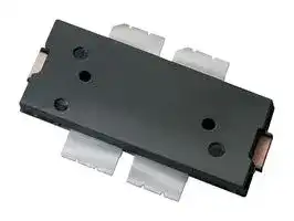


MRFE6VP5300NR1
RF FET Transistor, 140 V, 909 W, 1.8 MHz, 600 MHz, TO-270WB
- Manufacturer: NXP
- Product type: RF FETs
- Drain Source Voltage Vds:140V; Continuous Drain Current Id:-; Power Dissipation Pd:909W; Operating Frequency Min:1.8MHz; Operating Frequency Max:600MHz; RF Transistor Case:TO-270WB; No.
- MSL: MSL 3 - 168 hours
- SVHC: No SVHC (27-Jun-2018)
- No. of Pins: 4Pins
- Channel Type: N Channel
- Product Range: -
- Power Dissipation: 909W
- Transistor Mounting: Flange
- Transistor Case Style: TO-270WB
- Operating Frequency Max: 600MHz
- Operating Frequency Min: 1.8MHz
- Drain Source Voltage Vds: 140V
- Operating Temperature Max: 225°C
- Continuous Drain Current Id: -
| Delivery and price | |
|---|---|
| Units per pack | 1 |
| Price | 48.65 € |
| Current stock | 10+ |
| Lead time | 30 days |
**Freescale Semiconductor** Technical Data
Document Number: MRFE6VP5300N Rev. 1, 6/2014
## **RF Power LDMOS Transistors** High Ruggedness N--Channel Enhancement--Mode Lateral MOSFETs
These high ruggedness devices are designed for use in high VSWR industrial (including laser and plasma exciters), broadcast (analog and digital), aerospace and radio/land mobile applications. They are unmatched input and output designs allowing wide frequency range utilization, between 1.8 and 600 MHz.
## **MRFE6VP5300NR1 MRFE6VP5300GNR1**
**1.8–600 MHz, 300 W CW, 50 V WIDEBAND RF POWER LDMOS TRANSISTORS**
**Typical Performance:** VDD = 50 Vdc
|**Typical Performance:**VDD = 50 VdcDD = 50 Vdc= 50 Vdc|**Typical Performance:**VDD = 50 VdcDD = 50 Vdc= 50 Vdc|**Typical Performance:**VDD = 50 VdcDD = 50 Vdc= 50 Vdc|**Typical Performance:**VDD = 50 VdcDD = 50 Vdc= 50 Vdc|**Typical Performance:**VDD = 50 VdcDD = 50 Vdc= 50 Vdc|||
|---|---|---|---|---|---|---|
|**Frequency**<br>**(MHz)**<br>**Signal Type**<br>**Pout**<br>**(W)**<br>**Gps**<br>**(dB)**<br>87.5--108 **(1,3)**<br>CW<br>361<br>23.8<br>230 **(2)**<br>CW<br>300<br>25.0<br>230 **(2)**<br>Pulse (100sec, 20%<br>Duty Cycle)<br>300 Peak<br>27.0<br>**Load Mismatch/Ruggedness**<br>~~————~~||||||**D**<br>**(%)**<br>80.1<br>70.0<br>71.0|
|**Frequency**||**Pin**||**Test**|||
|**(MHz)**<br>**Signal Type**<br>**VSWR**||**(W)**||**Voltage**||**Result**|
|98 **(1)**<br>CW<br>> 65:1||3||50||No Device|
|at all Phase||(3 dB|||Degradation||
|Angles||Overdrive)|||||
|230 **(2)**<br>Pulse||1.16 Peak|||||
|(100sec, 20%<br>Duty Cycle)||(3 dB<br>Overdrive)|||||
1. Measured in 87.5–108 MHz broadband reference circuit.
2. Measured in 230 MHz narrowband test circuit.
3. The values shown are the minimum measured performance numbers across the indicated frequency range.
## **Features**
- Wide Operating Frequency Range
- Extreme Ruggedness
- Unmatched Input and Output Allowing Wide Frequency Range Utilization
- Integrated Stability Enhancements
- Low Thermal Resistance
**==> picture [146 x 112] intentionally omitted <==**
**----- Start of picture text -----**<br>
TO--270WB--4<br>PLASTIC<br>MRFE6VP5300NR1<br>TO--270WBG--4<br>PLASTIC<br>MRFE6VP5300GNR1<br>**----- End of picture text -----**<br>
**==> picture [156 x 117] intentionally omitted <==**
**----- Start of picture text -----**<br>
Gate A 3 2 Drain A<br>‘ia :<br>Gate B 4 1 Drain B<br>| ne |<br>{ eat<br>(Top View)<br>Note: Exposed backside of the package is<br>the source terminal for the transistors.<br>**----- End of picture text -----**<br>
**Figure 1. Pin Connections**
- Integrated ESD Protection Circuitry
- In Tape and Reel. R1 Suffix = 500 Units, 44 mm Tape Width, 13--inch Reel.
**MRFE6VP5300NR1 MRFE6VP5300GNR1** ~~=freescale~~
Freescale Semiconductor, Inc., 2014. All rights reserved.
RF Device Data Freescale Semiconductor, Inc.
1
**Table 1. Maximum Ratings**
**Rating Symbol Value Unit** Drain--Source Voltage VDSS –0.5, +133 Vdc Gate--Source Voltage VGS –6.0, +10 Vdc Storage Temperature Range Tstg –65 to +150 C Case Operating Temperature Range TC –40 to +150 C Operating Junction Temperature Range **[(1,2)]** TJ –40 to +225 C Total Device Dissipation @ TC = 25C PD 909 W Derate above 25C 4.55 W/C ~~eee~~ **Table 2. Thermal Characteristics Characteristic Symbol Value[(2,3)] Unit** Thermal Resistance, Junction to Case RJC 0.22 C/W CW: Case Temperature 81C, 305 W CW, 50 Vdc, IDQ(A+B) = 100 mA, 230 MHz Thermal Impedance, Junction to Case ZJC 0.034 C/W Pulse: Case Temperature 59C, 300 W Peak, 100 sec Pulse Width, ~~——==e~~ 20% Duty Cycle, 50 Vdc, IDQ(A+B) = 100 mA, 230 MHz **Table 3. ESD Protection Characteristics Test Methodology Class** Human Body Model (per JESD22--A114) 2, passes 2500 V Machine Model (per EIA/JESD22--A115) A, passes 150 V Charge Device Model (per JESD22--C101) IV, passes 2000 V **Table 4. Moisture Sensitivity Level Test Methodology Rating Package Peak Temperature Unit** Per JESD22--A113, IPC/JEDEC J--STD--020 3 260 C ~~a~~ **Table 5. Electrical Characteristics** (TA = 25C unless otherwise noted) **Characteristic Symbol Min Typ Max Unit Off Characteristics[(4)]** Gate--Source Leakage Current IGSS — — 1 Adc (VGS = 5 Vdc, VDS = 0 Vdc) Drain--Source Breakdown Voltage V(BR)DSS 133 140 — Vdc (VGS = 0 Vdc, ID = 50 mA) Zero Gate Voltage Drain Leakage Current IDSS — — 5 Adc (VDS = 50 Vdc, VGS = 0 Vdc) Zero Gate Voltage Drain Leakage Current IDSS — — 10 Adc (VDS = 100 Vdc, VGS = 0 Vdc) ~~EE~~ **On Characteristics** Gate Threshold Voltage VGS(th) 1.8 2.3 2.8 Vdc (VDS = 10 Vdc, ID = 960 Adc) Gate Quiescent Voltage VGS(Q) 2.2 2.7 3.2 Vdc (VDD = 50 Vdc, ID = 100 mAdc, Measured in Functional Test) Drain--Source On--Voltage VDS(on) — 0.26 — Vdc (VGS = 10 Vdc, ID = 2 Adc) ~~SS~~ 1. Continuous use at maximum temperature will affect MTTF. 2. MTTF calculator available at http://www.freescale.com/rf. Select Software & Tools/Development Tools/Calculators to access MTTF calculators by product.
3. Refer to AN1955, _Thermal Measurement Methodology of RF Power Amplifiers._ Go to http://www.freescale.com/rf. Select Documentation/Application Notes -- AN1955.
4. Each side of device measured separately.
(continued)
**MRFE6VP5300NR1 MRFE6VP5300GNR1**
RF Device Data Freescale Semiconductor, Inc.
2
**Table 5. Electrical Characteristics** (TA = 25C unless otherwise noted) **(continued)**
|**Table 5. Electrical Characteristics** (TA = 25C unless otherwise noted)A = 25C unless otherwise noted)= 25C unless otherwise noted)C unless otherwise noted)C unless otherwise noted)**(continued)**|||
|---|---|---|
|**Characteristic**<br>**Symbol**<br>**Min**<br>**Typ**|**Max**|**Unit**|
|**Dynamic Characteristics (1)**|||
|Reverse Transfer Capacitance<br>Crss<br>—<br>1.4|—|pF|
|(VDS= 50 Vdc30 mV(rms)ac @ 1 MHz, VGS= 0 Vdc)|||
|Output Capacitance<br>Coss<br>—<br>63|—|pF|
|(VDS= 50 Vdc30 mV(rms)ac @ 1 MHz, VGS= 0 Vdc)|||
|Input Capacitance<br>Ciss<br>—<br>168|—|pF|
|(VDS= 50 Vdc, VGS= 0 Vdc30 mV(rms)ac @ 1 MHz)|||
|**Functional Tests (2)** (In Freescale Test Fixture, 50 ohm system) VDD= 50 Vdc, IDQ(A+B)= 100 mA, Pout= 300 W Peak (60 W Avg.),|= 300 W Peak (60 W Avg.),||
|f = 230 MHz, 100sec Pulse Width, 20% Duty Cycle|||
|Power Gain<br>Gps<br>26.0<br>27.0<br>28.5<br>dB<br>Drain Efficiency<br>D<br>69.0<br>71.0<br>—<br>%<br>Input Return Loss<br>IRL<br>—<br>–20<br>–9<br>dB<br>**Table 6. Load Mismatch/Ruggedness** (In Freescale Test Fixture, 50 ohm system) IDQ(A+B)= 100 mA<br>**Frequency**<br>**(MHz)**<br>**Signal Type**<br>**VSWR**<br>**Pin**<br>**(W)**<br>**Test Voltage, VDD**<br>**Result**<br>230<br>Pulse<br>(100sec, 20% Duty Cycle)<br>> 65:1 at all<br>Phase Angles<br>1.16 Peak<br>(3 dB Overdrive)<br>50<br>No Device Degradation<br>1. Each side of device measured separately.<br>2. Measurements made with device in straight lead configuration before any lead forming operation is applied. Lead forming is used for gull wing<br>(GN) parts.<br>~~ee~~|||
**MRFE6VP5300NR1 MRFE6VP5300GNR1**
RF Device Data Freescale Semiconductor, Inc.
3
## **TYPICAL CHARACTERISTICS**
**==> picture [498 x 249] intentionally omitted <==**
**----- Start of picture text -----**<br>
500 1.06<br>Measured with 30 mV(rms)ac @ 1 MHz 1.05 500 mA VDD = 50 Vdc<br>Oe V GS = 0 Vdc C iss 1.04 Oe I DQ(A+B) = 100 mA<br>100 SSA 1.03 aAN<br>1.02 1500 mA<br>Coss 1.01<br>2500 mA<br>———— 1 Ne<br>0.99<br>10 A ee ee ee ee ee<br>0.98<br>SSSS=—=a 0.97 FoNX s<br>nn, ann es 0.96 eseS<br>se Crss 0.95 ss<br>1 Cd —Tr ee 0.94 ns<br>0 10 20 30 40 50 --50 --25 0 25 50 75 100<br>VDS, DRAIN--SOURCE VOLTAGE (VOLTS) TC, CASE TEMPERATURE (C)<br>Note: Each side of device measured separately. IDQ (mA) Slope (mV/ C)<br>Figure 2. Capacitance versus Drain--Source Voltage 100 –2.651<br>500 –2.158<br>1500 –1.977<br>2500 –1.787<br>GS(Q)<br>NORMALIZED V<br>C, CAPACITANCE (pF)<br>**----- End of picture text -----**<br>
**==> picture [187 x 21] intentionally omitted <==**
**----- Start of picture text -----**<br>
Figure 3. Normalized VGS versus Quiescent<br>Current and Case Temperature<br>**----- End of picture text -----**<br>
**==> picture [239 x 232] intentionally omitted <==**
**----- Start of picture text -----**<br>
10 [8]<br>SS ID = 6.38 Amps = VDD = 50 Vdc<br>10 [7]<br>———<br>10 [6] 8.04 Amps<br>Hilt)UL SS<br>9.61 Amps<br>Sa e e<br>10 [5]<br>ptf | tt} tf<br>Se<br>10 [4] Pi tT t>_ TT tet tT tT Et dT tT ff<br>90 110 130 150 170 190 210 230 250<br>TJ, JUNCTION TEMPERATURE (C)<br>Note: MTTF value represents the total cumulative operating time<br>under indicated test conditions.<br>MTTF calculator available at http:/www.freescale.com/rf. Select<br>Software & Tools/Development Tools/Calculators to access MTTF<br>calculators by product.<br>MTTF (HOURS)<br>**----- End of picture text -----**<br>
**Figure 4. MTTF versus Junction Temperature -- CW**
**MRFE6VP5300NR1 MRFE6VP5300GNR1**
RF Device Data Freescale Semiconductor, Inc.
4
## **230 MHz NARROWBAND PRODUCTION TEST FIXTURE**
**==> picture [444 x 294] intentionally omitted <==**
**----- Start of picture text -----**<br>
C3 C5<br>00000000000° 4) eceeesioocccocc00== 4) 2200000000 (f) 0000000000000000(4)— 0000 Jo go (4)<br>° o ° 8 I yy |e 4 MRFE6VP5300N —e e C27 I C29<br>° o ° i | B1 C7 Rev. 2 C21 C23<br>° 8° co L vA Va<br>° oo004 0000000000<br>O° anoo rer mnomemememememememenemememenenemonemenenenomenenemenonenene)<br>: C1 @ er D49840 6 “<br>8 of ee Lh No C19 q| || C25<br>°° L1 000/f °° oooooo| [ETEP jo7<br>°° COAX1 C11 °° °000000 L4 Sb |°° COAX3<br>°° ° 0000oO ° ° oo000008 fe)8° ©<br>8 °°<br>°°° ®®z°e000000000000000<br>°oo00000 —iy} C9 l] I} C14 ooo0jo00 C17<br>C13<br>—, 9 LIT = 5 C16 = bo ot<br>L3<br>000000° jw® C10 l] | C15 i n n 0000/00 C18<br>° e<br>°3 ° O v%4 8 0000 0000000000000000O°8°<br>°°<br>°° 3}° 000000 °8<br>°° COAX2 L2 C12 O°°}° 000000° L5 _EP fe)}jo COAX4<br>8 ood 8 000000] Fi FEY lo C26<br>8°° C2 oo6 fS|/ 5000 py’44 ° Je C20 °Qdl | 0 00000000000000000000000000000—<br>° ° 000g ° foco00000000 9?<br>°St ° °° B2 — .)? C8 __ C22 C24 Ta<br>°°°000000000 ° © (F) 000000l0000000000 C4 LET C6 Je (F) ® cccceccccccc0000(#) P — Tooo} C28 °%i C30 $o(4)<br>CUT OUT AREA<br>**----- End of picture text -----**<br>
**Figure 5. MRFE6VP5300NR1 Narrowband Test Circuit Component Layout — 230 MHz**
**MRFE6VP5300NR1 MRFE6VP5300GNR1**
RF Device Data Freescale Semiconductor, Inc.
5
## **230 MHz NARROWBAND PRODUCTION TEST FIXTURE**
**Table 7. MRFE6VP5300NR1 Narrowband Test Circuit Component Designations and Values — 230 MHz**
|**Part**<br>~~eG~~<br>~~ee~~|**Description**<br>~~eG~~<br>~~G~~|**Part Number**<br>~~eG~~|**Manufacturer**<br>~~eG~~|
|---|---|---|---|
|B1, B2<br>~~eG~~<br>~~ee~~|Small Ferrite Beads, Surface Mount<br>~~eG~~<br>~~G~~|2743019447<br>~~eG~~|Fair-Rite<br>~~eG~~|
|C1, C2<br>~~ee~~<br>~~GG~~|22F, 35 V Tantulum Capacitors<br>~~G~~<br>~~GG~~|T491X226K035AT<br>~~GG~~|Kemet<br>~~GG~~|
|C3, C4<br>~~GC~~|0.1F Chip Capacitors<br>~~GC~~|CDR33BX104AKWS<br>~~GC~~|AVX<br>~~GC~~|
|C5, C6<br>~~GG~~|220 nF Chip Capacitors<br>~~GG~~|C1812C224K5RACTU<br>~~GG~~|Kemet<br>~~GG~~|
|C7, C8<br>~~GC~~|2.2F Chip Capacitors<br>~~GC~~|C1825C225J5RACTU<br>~~GC~~|Kemet<br>~~GC~~|
|C9, C10, C11, C12<br>~~GO~~|1000 pF Chip Capacitors<br>~~GO~~|ATC100B102JT50XT<br>~~GO~~|ATC<br>~~GO~~|
|C13<br>~~GG~~|75 pF Chip Capacitor<br>~~GG~~|ATC100B750JT500XT<br>~~GG~~|ATC<br>~~GG~~|
|C14, C15<br>~~GC~~|680 pF Chip Capacitors<br>~~GC~~|ATC100B681JT200XT<br>~~GC~~|ATC<br>~~GC~~|
|C16<br>~~GC~~<br>~~CC~~|82 pF Chip Capacitor<br>~~GC~~<br>~~CC~~|ATC100B820JT500XT<br>~~GC~~<br>~~CC~~|ATC<br>~~GC~~<br>~~CC~~|
|C17<br>~~CC~~<br>~~Ge~~|8.2 pF Chip Capacitor<br>~~CC~~<br>~~Ge~~|ATC100B8R2CT500XT<br>~~CC~~<br>~~Ge~~|ATC<br>~~CC~~<br>~~Ge~~|
|C18<br>~~Ge~~<br>~~GO~~|11 pF Chip Capacitor<br>~~Ge~~<br>~~GO~~|ATC100B110JT500XT<br>~~Ge~~<br>~~GO~~|ATC<br>~~Ge~~<br>~~GO~~|
|C19, C20<br>~~GG~~|240 pF Chip Capacitors<br>~~GG~~|ATC100B241JT200XT<br>~~GG~~|ATC<br>~~GG~~|
|C21, C22<br>~~GG~~<br>~~Ce~~|0.10F Chip Capacitors<br>~~GG~~<br>~~Ce~~|C1812F104K1RACTU<br>~~GG~~<br>~~Ce~~|Kemet<br>~~GG~~<br>~~Ce~~|
|C23, C24<br>~~Ce~~<br>~~GG~~|0.1F Chip Capacitors<br>~~Ce~~<br>~~GG~~|CDR33BX104AKWS<br>~~Ce~~<br>~~GG~~|AVX<br>~~Ce~~<br>~~GG~~|
|C25, C26<br>~~GG~~<br>~~GG~~|2.2F Chip Capacitors<br>~~GG~~<br>~~GG~~|2225X7R225KJT3AB<br>~~GG~~<br>~~GG~~|ATC<br>~~GG~~<br>~~GG~~|
|C27, C28, C29, C30<br>~~GC~~|470F, 63 V Electrolytic Capacitors<br>~~GC~~|MCGPR63V477M13X26-RH<br>~~GC~~|Multicomp<br>~~GC~~|
|Coax1, 2, 3, 4<br>~~GG~~|25Semi Rigid Coax, 2.4<br>~~GG~~|UT-141C-25<br>~~GG~~|Micro-Coax<br>~~GG~~|
|L1, L2<br>~~GC~~|12 nH Inductors, 3 Turns<br>~~GC~~|GA3094-ALC<br>~~GC~~|Coilcraft<br>~~GC~~|
|L3<br>~~GO~~|22 nH Inductor<br>~~GO~~|1812SMS-22NJLC<br>~~GO~~|Coilcraft<br>~~GO~~|
|L4, L5<br>~~GO~~|17.5 nH Inductors, 4 Turns<br>~~GO~~|GA3095-ALC<br>~~GO~~|Coilcraft<br>~~GO~~|
|PCB<br>~~GC~~|Arlon AD255A 0.030,r= 2.55<br>~~GC~~|D49840<br>~~GC~~|MTL<br>~~GC~~|
**MRFE6VP5300NR1 MRFE6VP5300GNR1**
RF Device Data Freescale Semiconductor, Inc.
6
**==> picture [507 x 598] intentionally omitted <==**
**----- Start of picture text -----**<br>
ll<br>aol<br>aT<br>C i C H<br>H I C H<br>aT aT<br>4! E4l<br>F4! r rT FH<br>eal eal<br>| i<br>| --__] | -—-__]<br>i I i<br>" q q < =<br>|_| | -*_]<br>4 h! | | t l<br>L tt 4<br>L H L H<br>i) i)<br>E 4k E 4l<br>|!<br>RF<br>OUTPUT<br>Z30<br>C18<br>Z29<br>Z28 C17 Microstrip Microstrip Microstrip Microstrip Microstrip<br>0.230 0.230 0.082 0.082 0.082<br>DD DD Description<br>V+ C29 COAX3 COAX4 V+ C30 0.057 0.199 0.155 0.110 0.100<br>+ C27 + C28<br>C25 Z26 C16 Z27 C26<br>Microstrip Z24, Z25 Z26, Z27 Z28 Z29 Z30 * Line length include microstrip bends<br>C23 C24<br>Z24 Z25<br>C21 C14 C15 C22<br>Z22 C13 Z23 Microstrip Microstrip Microstrip Microstrip Microstrip Microstrip<br>C19 C20<br>0.746 0.522 0.150 0.150 0.230 0.230<br>L4 Z18 Z16 Z20 Z21 Z17 Z19 L5 Description <br>Z14 Z15 0.361 0.289 0.347 0.329 0.060 1.040<br>DUT<br>Microstrip Z12, Z13 Z14, Z15 Z16, Z17 Z18, Z19 Z20, Z21 Z22, Z23<br>Z12 L3 Z13<br>L1 C11 Z10 Z11 C12 L2<br>Microstrip Microstrip Microstrip Microstrip Microstrip Microstrip<br>C7 Z8 Z6 Z4 Z5 Z7 Z9 C8 0.082 0.120 0.120 0.058 0.068 0.746<br>C5 C9 C10 C6 Figure 6. MRFE6VP5300NR1 Narrowband Test Circuit Schematic — 230 MHz Description<br> <br>Z2 Z3<br>C3 C4<br>0.366 0.169 0.432 0.655 0.252 0.078<br>B1 B2<br>+ C1 + C2<br>COAX1 COAX2<br>Microstrip Z1 Z2, Z3 Z4, Z5 Z6*, Z7* Z8, Z9 Z10, Z11<br>Table 8. MRFE6VP5300NR1 Narrowband Test Circuit Microstrips — 230 MHz<br>GG GG<br>V Z1 V<br>RF<br>INPUT<br>**----- End of picture text -----**<br>
**MRFE6VP5300NR1 MRFE6VP5300GNR1**
RF Device Data Freescale Semiconductor, Inc.
7
**TYPICAL CHARACTERISTICS — 230 MHz**
**==> picture [242 x 172] intentionally omitted <==**
**----- Start of picture text -----**<br>
350<br>VDD = 50 Vdc, f = 230 MHz<br>300 Pulse Width = 100 sec, 20% Duty Cycle<br>250 CAE<br>Pin = 0.64 W<br>200<br>eeZe Pin = 0.32 W<br>150 P| aA<br>100<br>pf | [7 sf<br>50 | | y ist |<br>0 |ip| |7L |YY et| ct<br>0 0.5 1 1.5 2 2.5 3 3.5<br>VGS, GATE--SOURCE VOLTAGE (VOLTS)<br>, OUTPUT POWER (WATTS) PEAK<br>out<br>P<br>**----- End of picture text -----**<br>
**Figure 7. Output Power versus Gate--Source Voltage at a Constant Input Power**
**==> picture [510 x 423] intentionally omitted <==**
**----- Start of picture text -----**<br>
60 31 90<br>58 V Pulse Width = 100 DD = 50 Vdc, IDQ(A+B) sec, 20% Duty Cycle = 100 mA, f = 230 MHz Ty 30 V Pulse Width = 100 DD = 50 Vdc, IDQ(A+B) sec, 20% Duty Cycle = 100 mA, f = 230 MHz 80<br>56<br>29 D 70<br>54 IDQ(A+B) = 900 mA<br>52 Terrace} 28 lig 60<br>600 mA<br>50 es 27 ee A 50<br>48 pot | wt | ft 26 TM 300 mA ATHY 40<br>46<br>pf 25 | ON. 30<br>44 a A tt 100 mA a 900 mA Gps<br>42 i a 24 Atl 600 mA 20<br>100 mA 300 mA<br>40 ALI 23 | AT | Hitt 10<br>16 18 20 22 24 26 28 30 32 10 100 500<br>Pin, INPUT POWER (dBm) Pout, OUTPUT POWER (WATTS) PEAK<br>f P1dB P3dB Figure 9. Power Gain and Drain Efficiency<br>(MHz) (W) (W) versus Output Power and Quiescent Current<br>230 313 370<br>Figure 8. Output Power versus Input Power<br>30 90 29<br>VDD = 50 Vdc, IDQ(A+B) = 100 mA, f = 230 MHz --40 _ C<br>29 Pulse Width = 100 sec, 20% Duty Cycle LN 80 28 ee<br>27<br>28 25 _ C 70<br>26<br>27 TC = --40 _ C pe 60 ee<br>25<br>26 OGZO 50 24 ESSAFROIN ONE XD 50 V<br>_ 45 V<br>25 25 _ C 72 D ANING 85 C 40 23 PF. 4ARRG 40 V TY<br>atl) ee FAA A<br>24 85 _ C 30 22 35 V<br>Gps 21<br>23 Ze |W 20 20 AOE VDD = 30 V I DQ(A+B) = 100 mA, f = 230 MHz<br>Pulse Width = 100 sec, 20% Duty Cycle<br>22 TTISLT Tt | tt 10 19 eeFTfT<br>10 100 500 0 50 100 150 200 250 300 350 400<br>Pout, OUTPUT POWER (WATTS) PEAK Pout, OUTPUT POWER (WATTS) PEAK<br>, POWER GAIN (dB)<br>ps DRAIN EFFICIENCY (%)<br>G D,<br>, OUTPUT POWER (dBm) PEAK <br>out<br>P<br>, POWER GAIN (dB) , POWER GAIN (dB)<br>Gps DRAIN EFFICIENCY (%)D, Gps<br><br>**----- End of picture text -----**<br>
**Figure 10. Power Gain and Drain Efficiency versus CW Output Power**
**Figure 11. Power Gain versus Output Power and Drain--Source Voltage**
**MRFE6VP5300NR1 MRFE6VP5300GNR1**
RF Device Data Freescale Semiconductor, Inc.
8
## **230 MHz NARROWBAND PRODUCTION TEST FIXTURE**
**==> picture [308 x 182] intentionally omitted <==**
**----- Start of picture text -----**<br>
VDD = 50 Vdc, IDQ(A+B) = 100 mA, Pout = 300 W Peak<br>f Zsource Zload<br>MHz <br>230 1.50 – j10.70 8.30 + j6.90<br>| Zsource = Test circuit impedance as measured from __} _|<br>gate to gate, balanced configuration.<br>Zload = Test circuit impedance as measured from<br>drain to drain, balanced configuration.<br>Input Device Output<br>Matching + Under -- Matching<br>50 Network Test Network 50 <br>Li -- t t + l<br>h t<br>Zsource Zload<br>**----- End of picture text -----**<br>
**Figure 12. Narrowband Series Equivalent Source and Load Impedance — 230 MHz**
**MRFE6VP5300NR1 MRFE6VP5300GNR1**
RF Device Data Freescale Semiconductor, Inc.
9
## **87.5–108 MHz BROADBAND REFERENCE CIRCUIT**
**Table 9. 87.5–108 MHz Broadband Performance** (In Freescale Reference Circuit, 50 ohm system) VDD = 50 Vdc, IDQ(A+B) = 100 mA, Pin = 1.5 W, CW
|**Frequency**<br>**(MHz)**<br>**Gps**<br>**(dB)**<br>**D**<br>**(%)**<br>**Pout**<br>**(W)**<br>87.5<br>24.4<br>80.1<br>415<br>98<br>24.3<br>81.8<br>404<br>108<br>23.8<br>80.5<br>361<br>~~——_———~~|
|---|
|**Table 10. Load Mismatch/Ruggedness** (In Freescale Reference Circuit, 50 ohm system) IDQ(A+B)= 100 mA|
|**Frequency**<br>**(MHz)**<br>**Signal Type**<br>**VSWR**<br>**Pin**<br>**(W)**<br>**Test Voltage, VDD**<br>**Result**<br>98<br>CW<br>> 65:1<br>at all Phase Angles<br>3<br>(3 dB Overdrive)<br>50<br>No Device<br>Degradation<br>~~—————~~|
**MRFE6VP5300NR1 MRFE6VP5300GNR1**
RF Device Data Freescale Semiconductor, Inc.
10
## **87.5–108 MHz BROADBAND REFERENCE CIRCUIT**
**==> picture [443 x 283] intentionally omitted <==**
**----- Start of picture text -----**<br>
R5* R6* R4* ) C1* eyf COAX1 — Qoooco000007 a —<br>a ‘@ ) HO MQAE+S a es R11* X OPO C14 PO C15 P f C16 Vo<br>C3* A O R3* O C00 0 /0000 ea l 7 R10* YT oe + °<br>C13<br>D59349 ) R8 (+ R7* LErin g Y oo U1* oosos n s iy C12 v 88<br>| Ae pte... © I H °<br>C2*<br>O [Ald ©o©o000 nels O<br>O R1* ptaetin o0004 C11 5 a<br>R2*<br>U2*<br>cc) C4 grees / | [| C6 6<br>00000000000" -— _ : cS) F<br>ya an R9 _ HL C8 a<br>a p: T1 fax | Q1 D) Ll e i He ( \o00<br>(ee) C5 C17 L1 nye C9 nin<br>0900000000 Ss =o a | I a C7 eal 4k [| ] 00000<br>i ) °©d00000 = ® o88 o<br>; 3o000000000000 0000) SS 50 HD<br>COAX3<br>2 f reescale’ © O e = 38<br>semiconductor O exomonononeneonononenene)<br>MRFE6VP5300N<br>© © Rev. 1 © ) io ) ©<br>(_ (_ COAX2<br>Note: Component number C10 is not used.<br>* Bias Regulator and Temperature Compensation. Refer to AN1643, RF LDMOS Power Modules for GSM Base Station<br>Application: Optimum Biasing Circuit . Go to http://www.freescale.com/rf. Select Documentation/Application Notes – AN1643.<br>**----- End of picture text -----**<br>
**Figure 13. MRFE6VP5300NR1 Broadband Reference Circuit Component Layout — 87.5–108 MHz**
**MRFE6VP5300NR1 MRFE6VP5300GNR1**
RF Device Data Freescale Semiconductor, Inc.
11
## **87.5–108 MHz BROADBAND REFERENCE CIRCUIT**
**Table 11. MRFE6VP5300NR1 Broadband Reference Circuit Component Designations and Values — 87.5–108 MHz**
|**Part**<br>~~eG~~|**Description**<br>~~eG~~|**Part Number**<br>~~eG~~|**Manufacturer**<br>~~eG~~|
|---|---|---|---|
|C1, C2<br>~~eG~~<br>~~eG~~|1F Chip Capacitors<br>~~eG~~<br>~~eG~~|GRM31CR72A105KA01L<br>~~eG~~<br>~~GO~~|Murata<br>~~eG~~<br>~~GO~~|
|C3<br>~~eG~~<br>~~GG~~|10 nF Chip Capacitor<br>~~eG~~<br>~~GG~~|ATC200B103KT50XT<br>~~GO~~<br>~~GG~~|ATC<br>~~GO~~<br>~~GG~~|
|C4<br>~~GG~~<br>~~GG~~|150 pF Chip Capacitor<br>~~GG~~<br>~~GG~~|ATC100B151JT300XT<br>~~GG~~<br>~~GG~~|ATC<br>~~GG~~<br>~~GG~~|
|C5<br>~~GG~~|20 pF Chip Capacitor<br>~~GG~~|ATC100B200JT500XT<br>~~GG~~|ATC<br>~~GG~~|
|C6, C8, C9<br>~~GG~~|1000 pF Chip Capacitors<br>~~GG~~|ATC200B102KT50XT<br>~~GG~~<br>~~Ge~~|ATC<br>~~GG~~|
|C7<br>~~eG~~|560 pF Chip Capacitor<br>~~eG~~|ATC100B561KT50XT<br>~~eG~~<br>~~Ge~~|ATC<br>~~eG~~|
|C11<br>~~pf~~|10 nF Chip Capacitor<br>~~pf~~|GCJ216R72A103KA01D<br>~~Ge~~<br>~~pf~~<br>~~GO~~|Murata<br>~~pf~~|
|C12<br>~~eG~~|47 nF Chip Capacitor<br>~~eG~~|GCJ21BR72A473KA01L<br>~~eG~~<br>~~GO~~|Murata<br>~~eG~~|
|C13<br>~~eG~~|470 nF Chip Capacitor<br>~~eG~~|GRM31MR72A474KA01L<br>~~GO~~<br>~~eG~~|Murata<br>~~eG~~|
|C14, C15<br>~~eG~~<br>~~ee~~|10F Chip Capacitors<br>~~eG~~<br>~~GG~~|C5750X7S2A106M230KB<br>~~eG~~<br>~~GG~~|TDK<br>~~eG~~<br>~~GG~~|
|C16<br>~~ee~~|470F, 63 V Electrolytic Capacitor<br>~~GG~~|MCGPR63V477M13X26<br>~~GG~~|Multicomp<br>~~GG~~|
|C17<br>~~ee~~<br>~~eG~~<br>~~Ge~~|20 pF Chip Capacitor<br>~~GG~~<br>~~eG~~<br>~~Ge~~|ATC100B200JT500XT<br>~~GG~~<br>~~eG~~<br>~~GO~~|ATC<br>~~GG~~<br>~~eG~~<br>~~GO~~|
|Coax1, 2<br>~~Ge~~|35Flex Cable, 4.72<br>~~Ge~~|HSF-141<br>~~GO~~|Hongsen Cable<br>~~GO~~|
|Coax3<br>~~Ge~~<br>~~GG~~<br>~~a~~|50Flex Cable, 6.3<br>~~Ge~~<br>~~GG~~<br>~~ee~~|SM141<br>~~GO~~<br>~~GG~~|Huber Suhner<br>~~GO~~<br>~~GG~~|
|L1<br>~~GG~~<br>~~a~~|5 Turns, #16 AWG ID = 0.315/8 mm Inductor,<br>Hand Wound<br>~~GG~~<br>~~ee~~|Copper Wire<br>~~GG~~|~~GG~~|
|Q1<br>~~a~~<br>~~GG~~|RF Power LDMOS Transistor<br>~~ee~~<br>~~GG~~|MRFE6VP5300NR1<br>~~GG~~|Freescale<br>~~GG~~|
|R1<br>~~Ge~~|2.2 k, 1/8 W Chip Resistor<br>~~Ge~~|CRCW08052K20FKEA<br>~~Ge~~|Vishay<br>~~Ge~~|
|R2<br>~~GG~~|390, 1/8 W Chip Resistor<br>~~GG~~|CRCW0805390RFKEA<br>~~GG~~|Vishay<br>~~GG~~|
|R3<br>~~GG~~|10, 1/8 W Chip Resistor<br>~~GG~~|CRCW080510R0FKEA<br>~~GG~~<br>~~Ge~~|Vishay<br>~~GG~~|
|R4<br>~~eG~~|1.0 k, 1/8 W Chip Resistor<br>~~eG~~|CRCW08051K00FKEA<br>~~eG~~<br>~~Ge~~<br>~~GO~~|Vishay<br>~~eG~~|
|R5<br>~~eG~~|2.7 k, 1/8 W Chip Resistor<br>~~eG~~|CRCW08052K70FKEA<br>~~Ge~~<br>~~eG~~<br>~~GO~~|Vishay<br>~~eG~~|
|R6<br>~~eG~~|200, 1/8 W Chip Resistor<br>~~eG~~|CRCW0805200RFKEA<br>~~GO~~<br>~~eG~~|Vishay<br>~~eG~~|
|R7<br>~~eG~~<br>~~ee~~|5.0 kMulti-turn Cermet Trimmer Potentiometer<br>~~eG~~<br>~~GG~~|3224W-1-502E<br>~~eG~~<br>~~GG~~|Bourns<br>~~eG~~<br>~~GG~~|
|R8<br>~~eG~~<br>~~ee~~<br>~~ee~~|10, 1/4 W Chip Resistor<br>~~eG~~<br>~~GG~~<br>~~GG~~|CRCW120610R0FKEA<br>~~eG~~<br>~~GG~~<br>~~GG~~|Vishay<br>~~eG~~<br>~~GG~~<br>~~GG~~|
|R9<br>~~ee~~<br>~~ee~~|240, 1/4 W Chip Resistor<br>~~GG~~<br>~~GG~~|CRCW1206240RFKEA<br>~~GG~~<br>~~GG~~|Vishay<br>~~GG~~<br>~~GG~~|
|R10<br>~~ee~~<br>~~eG~~|4.7 k, 1/2 W Chip Resistor<br>~~GG~~<br>~~eG~~|CRCW12104K70FKEA<br>~~GG~~<br>~~GO~~|Vishay<br>~~GG~~<br>~~GO~~|
|R11<br>~~eG~~<br>~~eG~~<br>~~a~~|5.1 k, 1/2 W Chip Resistor<br>~~eG~~<br>~~eG~~<br>~~ee~~|CRCW12105K10FKEA<br>~~GO~~<br>~~GO~~|Vishay<br>~~GO~~<br>~~GO~~|
|T1<br>~~eG~~<br>~~a~~|61 Material Binocular Core Ferrite (9:1) with<br>24 AWG 1 Turn Primary, 24 AWG 3 Turns<br>Secondary, Hand Wound<br>~~eG~~<br>~~ee~~|2861000202<br>~~GO~~<br>~~GO~~|Fair-Rite<br>~~GO~~|
|U1<br>~~a~~<br>~~Ge~~|Voltage Regulator 5 V, Micro8<br>~~ee~~<br>~~Ge~~|LP2951ACDMR2G<br>~~Ge~~<br>~~GO~~|ON Semiconductor<br>~~Ge~~|
|U2<br>~~Ge~~<br>~~GG~~|NPN Bipolar Transistor<br>~~Ge~~<br>~~GG~~|BC847ALT1G<br>~~Ge~~<br>~~GO~~<br>~~GG~~|ON Semiconductor<br>~~Ge~~<br>~~GG~~|
|PCB<br>~~GF~~|Rogers RO4350B, 0.030,r= 3.66<br>~~GF~~|D59349<br>~~GF~~|MTL<br>~~GF~~|
Note: Component number C10 is not used.
**MRFE6VP5300NR1 MRFE6VP5300GNR1**
RF Device Data Freescale Semiconductor, Inc.
12
**==> picture [369 x 645] intentionally omitted <==**
**----- Start of picture text -----**<br>
bs<br>obs<br>ey<br>—_<br>ar<br>-<br>RF<br>OUTPUT<br>DD<br>V Z20<br>+ C16<br>C15<br>COAX3<br>C14<br>C13<br>Z18 Z19<br>C12<br>C8 C9<br>C11<br>Microstrip Microstrip Microstrip Microstrip Microstrip Microstrip<br>Z16 Z17 <br>Z15 0.240 0.210 0.140 0.100 0.300 0.170<br>L1 C7 Description<br> <br>C6 0.400 0.170 0.680 0.200 0.230 0.190<br>Z13 Z14<br>COAX1 COAX2 Microstrip Z11, Z12 Z13, Z14 Z15 Z16*, Z17* Z18, Z19 Z20 * Line length includes microstrip bends<br>Z11 Z12<br>C17<br>Z9 Z10 Microstrip Microstrip Microstrip Microstrip Microstrip Microstrip Microstrip<br> <br>0.150 0.080 0.080 0.170 0.240 0.630 0.630<br>DUT Description<br> <br>Z7 Z8<br>R9 0.430 0.320 0.680 0.310 0.195 0.380 0.380<br>Bias Regulator and<br>Temperature Compensation C5<br>R8 Z3 Z4 Z5 Z6 Table 12. MRFE6VP5300NR1 Broadband Reference Circuit Microstrips — 87.5–108 MHz Microstrip Z1 Z2* Z3* Z4 Z5, Z6 Z7, Z8 Z9, Z10<br>Figure 14. MRFE6VP5300NR1 Broadband Reference Circuit Schematic — 87.5–108 MHz<br>T1<br>Z2<br>C4<br>Z1<br>RF<br>INPUT Note: Component number C10 is not used.<br>**----- End of picture text -----**<br>
**MRFE6VP5300NR1 MRFE6VP5300GNR1**
RF Device Data Freescale Semiconductor, Inc.
13
## **TYPICAL CHARACTERISTICS — 87.5–108 MHz BROADBAND REFERENCE CIRCUIT**
**==> picture [284 x 174] intentionally omitted <==**
**----- Start of picture text -----**<br>
26 90<br>VDD = 50 Vdc, Pin = 1.5 W, IDQ(A+B) = 100 mA<br>25.5 PoTT 80<br>D<br>24.525 RoanePi Tt | ttt tt ty 7060<br>23.524 pjPT Ttpt |eettt Pett 50450<br>Gps<br>23 PTT tT ety ey 400<br>22.5 PPT 350<br>Pout<br>22 Fi tT it ttteRtt py 300<br>86 88 90 92 94 96 98 100 102 104 106 108 110<br>f, FREQUENCY (MHz)<br>, DRAIN<br>D<br><br>EFFICIENCY (%)<br>, POWER GAIN (dB)<br>ps<br>G<br>, OUTPUT<br>out<br>P<br>POWER (WATTS)<br>**----- End of picture text -----**<br>
**Figure 15. Power Gain, Drain Efficiency and CW Output Power versus Frequency at a Constant Input Power**
**==> picture [501 x 173] intentionally omitted <==**
**----- Start of picture text -----**<br>
350 450<br>VDD = 50 Vdc VDD = 50 Vdc<br>300 Pin = 0.5 W | | | | y 400 P in = 1.0 W | | |fla<br>350<br>250<br>ee f = 98 MHz 300 f = 98 MHz<br>108 MHz<br>200 108 MHz<br>250<br>150 |er| | | | Y 200 eeSo yw GEa<br>150<br>100 P| | | A | | | tay | |<br>87.5 MHz 100<br>50 2 ee 87.5 MHz<br>50<br>0 | | [Lr] | | 0 Pe TTF OULU<br>0 0.5 1 1.5 2 2.5 3 3.5 0 0.5 1 1.5 2 2.5 3 3.5<br>VGS, GATE--SOURCE VOLTAGE (VOLTS) VGS, GATE--SOURCE VOLTAGE (VOLTS)<br>, OUTPUT POWER (WATTS) , OUTPUT POWER (WATTS)<br>out out<br>P P<br>**----- End of picture text -----**<br>
**Figure 16. CW Output Power versus Gate--Source Voltage at a Constant Input Power**
**Figure 17. CW Output Power versus Gate--Source Voltage at a Constant Input Power**
**MRFE6VP5300NR1 MRFE6VP5300GNR1**
RF Device Data Freescale Semiconductor, Inc.
14
## **TYPICAL CHARACTERISTICS — 87.5–108 MHz BROADBAND REFERENCE CIRCUIT**
**==> picture [235 x 249] intentionally omitted <==**
**----- Start of picture text -----**<br>
60<br>58 V DD = 50 Vdc<br>lDQ(A+B) = 100 mA<br>56 SScSS==<br>— | |<br>54 eer<br>52<br>f = 98 MHz<br>50 108 MHz<br>48 | lA _| |<br>87.5 MHz<br>4644 vw,ee[| |eee| eeeff<br>20 22 24 26 28 30 32 34<br>Pin, INPUT POWER (dBm)<br>f P1dB P3dB<br>(MHz) (W) (W)<br>87.5 346 429<br>98 293 379<br>108 240 355<br>, OUTPUT POWER (dBm)<br>out<br>P<br>**----- End of picture text -----**<br>
**Figure 18. CW Output Power versus Input Power**
**==> picture [254 x 175] intentionally omitted <==**
**----- Start of picture text -----**<br>
30 90<br>VDD = 50 Vdc D<br>28 lDQ(A+B) = 100 mA 80<br>f = 98 MHz<br>26 pe 70<br>|_|<br>24 108 MHz 60<br>87.5 MHz<br>22 aPitt ne 50<br>iibz [TW]<br>108 MHz Gps<br>20 40<br>ne? ae<br>98 MHz<br>18 87.5 MHz 30<br>16 pePte 20<br>30 50 100 200 300 500<br>Pout, OUTPUT POWER (WATTS)<br>, POWER GAIN (dB)<br>ps DRAIN EFFICIENCY (%)<br>G D,<br><br>**----- End of picture text -----**<br>
**Figure 19. Power Gain and Drain Efficiency versus CW Output Power**
**MRFE6VP5300NR1 MRFE6VP5300GNR1**
RF Device Data Freescale Semiconductor, Inc.
15
**==> picture [429 x 586] intentionally omitted <==**
**----- Start of picture text -----**<br>
87.5–108 MHz BROADBAND REFERENCE CIRCUIT<br>or oS ywa 2 2 . 2 4 [3 = af > ox<br>PK . Y 14 MEP cy Ze<br>LE OT LAYS<br>fY v Ors osQS Oo Zo = 25 <br>6 cS cS A a |<br>Eh o LebgSOK OSXn TSRD ES S<br>Zsource LE a, ZS<br>PY PLEREREEEE KK LDS LEH hy<br>ERE SO SW EH Tees<br>(3/'e//, LIS REEL f = 87.5 MHz KOS SSSA TAO<br>SH OL REREREE OO. A SKN f = 108 MHz O r TT<br>| KIS KLEE LSS SAAT PE<br>g FAL laSPEPEOLR BRL IKCK SOTa<br>eisShe IPE PIERSKOKIASS SSOSSSIEH see<br>&T bo) RRR POLE OSS CT<br>lol fe! & EERE f = 87.5 MHz ELT LORRI COSC TE<br>f/f BEELER ROR ZERIT SN LSE<br>| steel Zload SD f = 108 MHz ORSON<br>* Ggsisstsdussriras an eeu semen asae: PRL REE S<br>fe] km sarasdiriesiiit/ Mmguwecaeeiiss: ae Pe EE Re<br>PCAsousfsnepzsiizics: Maman eeeacasces CREE TERETE APE Rey<br>efeareeiiteiruri eueeapescttt]/ mg aeaneee Deaeee ee seee EB)<br>S oaH-FHHHtHH resistance4 COMPONENT! Zo SH/? L]eerewerem:| © &H Steee<br>al BECHER rec) on Conpiciance comment) BRenettemBeetnnit Get<br>VASic SSS<br>5 Supececcaautesesl eee aeeees<br> fo Wie Menmuecemereee |<br>oo ca ener<br>20) Co eee ewe asasiis<br>VDD = 50 Vdc, IDQ(A+B) = 100 mA, Pout = 300 W CW<br>f Zsource Zload<br>MHz <br>87.5 10.3 + j14.4 13.7 + j8.15<br>92 11.5 + j15.8 14.2 + j8.09<br>96 12.6 + j17.0 14.7 + j8.04<br>100 13.9 + j18.2 15.2 + j7.99<br>104 15.5 + j19.6 15.7 + j7.94<br>108 17.2 + j20.9 16.2 + j7.89<br>Zsource = Test circuit impedance as measured from<br>gate to gate, balanced configuration.<br>Zload = Test circuit impedance as measured<br>from drain to drain, balanced configuration.<br>Input Device Output<br>Matching + Under -- Matching<br>Network Test Network<br>50 50 <br>-- +<br>Zsource Zload<br>**----- End of picture text -----**<br>
**Figure 20. Broadband Series Equivalent Source and Load Impedance — 87.5–108 MHz**
**MRFE6VP5300NR1 MRFE6VP5300GNR1**
RF Device Data Freescale Semiconductor, Inc.
16
## **HARMONIC MEASUREMENTS — 87.5–108 MHz BROADBAND REFERENCE CIRCUIT**
**==> picture [462 x 179] intentionally omitted <==**
**----- Start of picture text -----**<br>
Sweep 10 of 10 F1 100 MHz<br>10.0 es H2 200 MHz --45.2 dB<br>—— Fundamental (F1) ~ H3 300 MHz --17.7 dB<br>0.0<br>|<br>H4 400 MHz --52.9 dB<br>--10.0 a<br>H5 500 MHz --29.0 dB<br>H3<br>e s<br>--20.0<br>H5<br>--30.0 11.984 sps H2 H3 H4 H5<br>Se a 11.851 fps<br>--40.0--50.0 Ol H2 H4 (200 MHz) –45.2 dB (300 MHz) –17.7 dB (400 MHz) –52.9 dB (500 MHz) –29.0 dB<br>--60.0 mor ge n<br>A me a cee<br>--70.0 a<br>Center: 300 MHz Span: 600 MHz<br>**----- End of picture text -----**<br>
**Figure 21. 100 MHz Harmonics @ 300 W CW**
**MRFE6VP5300NR1 MRFE6VP5300GNR1**
RF Device Data Freescale Semiconductor, Inc.
17
## **PACKAGE DIMENSIONS**
**MRFE6VP5300NR1 MRFE6VP5300GNR1**
RF Device Data Freescale Semiconductor, Inc.
18
**MRFE6VP5300NR1 MRFE6VP5300GNR1**
RF Device Data Freescale Semiconductor, Inc.
19
**MRFE6VP5300NR1 MRFE6VP5300GNR1**
RF Device Data Freescale Semiconductor, Inc.
20
**MRFE6VP5300NR1 MRFE6VP5300GNR1**
RF Device Data Freescale Semiconductor, Inc.
21
**MRFE6VP5300NR1 MRFE6VP5300GNR1**
RF Device Data Freescale Semiconductor, Inc.
22
**MRFE6VP5300NR1 MRFE6VP5300GNR1**
RF Device Data Freescale Semiconductor, Inc.
23
## **PRODUCT DOCUMENTATION, SOFTWARE AND TOOLS**
Refer to the following documents, software and tools to aid your design process.
## **Application Notes**
- AN1955: Thermal Measurement Methodology of RF Power Amplifiers
- AN1643: RF LDMOS Power Modules for GSM Base Station Application: Optimum Biasing Circuit
## **Engineering Bulletins**
- EB212: Using Data Sheet Impedances for RF LDMOS Devices
## **Software**
- Electromigration MTTF Calculator
- RF High Power Model
## **Development Tools**
- Printed Circuit Boards
For Software and Tools, do a Part Number search at http://www.freescale.com, and select the “Part Number” link. Go to the Software & Tools tab on the part’s Product Summary page to download the respective tool.
## **REVISION HISTORY**
The following table summarizes revisions to this document.
|**Revision**|**Date**|**Description**|
|---|---|---|
|0|Mar. 2014|<br>Initial Release of Data Sheet|
|1|June 2014|<br>Typical Performance table, 87.5–108 MHz: updated output power, gain and eff. values to reflect<br>performance of circuit, p. 1<br><br>Functional Tests table, narrowband circuit: corrected output power from (30 W Avg.) to (60 W Avg.), p. 3<br><br>Table 9, 87.5–108 MHz Reference Circuit Broadband Performance table: updated all values to reflect<br>performance of circuit, p. 10<br><br>Fig. 13, Broadband Reference Circuit Component Layout — 87.5–108 MHz: updated layout to increase<br>ease of use, p. 11<br><br>Table 11, Broadband Reference Circuit Component Designations and Values — 87.5–108 MHz: updated<br>R2 and R11 resistors, p. 12<br><br>Fig. 14, Broadband Reference Circuit Schematic — 87.5–108 MHz: updated schematic to reflect<br>temperature compensation, p. 13|
**MRFE6VP5300NR1 MRFE6VP5300GNR1**
RF Device Data Freescale Semiconductor, Inc.
24
## _**How to Reach Us:**_
**Home Page:** freescale.com
**Web Support:** freescale.com/support
Information in this document is provided solely to enable system and software implementers to use Freescale products. There are no express or implied copyright licenses granted hereunder to design or fabricate any integrated circuits based on the information in this document.
Freescale reserves the right to make changes without further notice to any products herein. Freescale makes no warranty, representation, or guarantee regarding the suitability of its products for any particular purpose, nor does Freescale assume any liability arising out of the application or use of any product or circuit, and specifically disclaims any and all liability, including without limitation consequential or incidental damages. “Typical” parameters that may be provided in Freescale data sheets and/or specifications can and do vary in different applications, and actual performance may vary over time. All operating parameters, including “typicals,” must be validated for each customer application by customer’s technical experts. Freescale does not convey any license under its patent rights nor the rights of others. Freescale sells products pursuant to standard terms and conditions of sale, which can be found at the following address: freescale.com/SalesTermsandConditions.
Freescale and the Freescale logo are trademarks of Freescale Semiconductor, Inc., Reg. U.S. Pat. & Tm. Off. All other product or service names are the property of their respective owners.
E 2014 Freescale Semiconductor, Inc.
**MRFE6VP5300NR1 MRFE6VP5300GNR1** & freescale
RF Device DataDocument Number: MRFE6VP5300N Freescale Semiconductor, Inc.Rev. 1, 6/2014
25
Updated at April 10, 2026
NXP Semiconductors is a global leader in secure connectivity solutions, driving innovation across the automotive, industrial, IoT, mobile, and communications infrastructure markets. By developing advanced, purpose-built technologies, NXP enables devices to sense, think, connect, and act intelligently, delivering rigorously tested components that make the connected world safer and more efficient. Within the semiconductor space, NXP is highly regarded for its extensive range of high-performance integrated circuits and discrete devices. The brand's portfolio excels in drivers and interfaces, featuring a comprehensive selection of I/O expanders designed to streamline complex system architectures. For demanding high-frequency and wireless applications, NXP provides industry-leading RF FETs and RF/PIN diodes engineered to deliver exceptional signal integrity, efficiency, and reliability. The NXP product lineup further extends to essential discrete components, including versatile bipolar transistors, JFETs, and small signal diodes optimized for precision switching and amplification. Additionally, the portfolio supports advanced automation and smart applications with precision IC sensors, such as MEMS accelerometers, alongside specialized power management solutions like AC/DC LED driver ICs and single MOSFETs for cutting-edge electronics design.
About Novapart
Novapart is a B2B electronic component broker specialising in stock shortages and cost reduction. We source hard-to-find parts and identify compliant alternatives across a catalogue of 410,000+ components from 500+ manufacturers.
Learn more →Stock Shortage Specialist
When a component is unavailable, discontinued or has an unacceptable lead time, we tap into our network of vetted European and Asian distributors to source what you need — without compromising on quality or traceability.
Request a quote →Compliant Alternatives
We identify pin-to-pin, electrically equivalent substitutes that meet the same certifications (RoHS, AEC-Q100, REACH) as your original specification — validated against datasheets, not just part numbers. Often at a lower cost.
BOM Analysis service →