


MRFE6VP5150GNR1
RF FET, 139V, 225DEG C, 952W
- Manufacturer: NXP
- Product type: RF FETs
- No. of Pins: 4Pins
- Channel Type: N Channel
- Power Dissipation: 952W
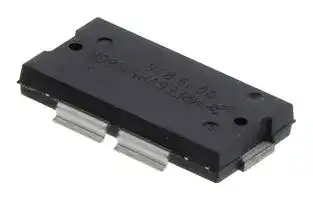
- RF Transistor Case: TO-270WB
- Transistor Mounting: Flange
- Power Dissipation Pd: 952W
- Transistor Case Style: TO-270WB
- Operating Frequency Max: 600MHz
- Operating Frequency Min: 1.8MHz
- Drain Source Voltage Vds: 139V
- Operating Temperature Max: 225°C
| Delivery and price | |
|---|---|
| Units per pack | 500 |
| Price | 32.75 € |
| Current stock | 10+ |
| Lead time | 7 days |
**Freescale Semiconductor** Technical Data
Document Number: MRFE6VP5150N Rev. 1, 7/2014
## **RF Power LDMOS Transistors** High Ruggedness N--Channel Enhancement--Mode Lateral MOSFETs
These high ruggedness devices are designed for use in high VSWR industrial (including laser and plasma exciters), broadcast (analog and digital), aerospace and radio/land mobile applications. They are unmatched input and output designs allowing wide frequency range utilization, between 1.8 and 600 MHz.
## **MRFE6VP5150NR1 MRFE6VP5150GNR1**
## **1.8–600 MHz, 150 W CW, 50 V WIDEBAND RF POWER LDMOS TRANSISTORS**
**Typical Performance:** VDD = 50 Vdc
|**Frequency**<br>**(MHz)**<br>**Signal Type**<br>87.5–108 **(1,3)**<br>CW<br>230 **(2)**<br>CW<br>230 **(2)**<br>Pulse<br>(100sec, 20%<br>Duty Cycle)<br>**Load Mismatch/Ruggedness**<br>**Frequency**<br>**(MHz)**<br>**Signal Type**<br>**VSWR**<br>~~———~~||**Pout**<br>**(W)**<br>179<br>150<br>150 Peak<br>**Pin**<br>**(W)**||**Gps**<br>**(dB)**<br>22.5<br>26.3<br>26.1<br>**Test**<br>**Voltage**|**D**<br>**(%)**<br>74.6<br>72.0<br>70.3<br>**Result**|
|---|---|---|---|---|---|
|98 **(1)**<br>CW<br>> 65:1||3.0||50|No Device|
|at all Phase||(3 dB|||Degradation|
|Angles||Overdrive)||||
|230 **(2)**<br>Pulse||0.62 Peak||||
|(100sec, 20%<br>Duty Cycle)||(3 dB<br>Overdrive)||||
1. Measured in 87.5–108 MHz broadband reference circuit.
2. Measured in 230 MHz narrowband test circuit.
3. The values shown are the minimum measured performance numbers across the indicated frequency range.
## **Features**
- Wide Operating Frequency Range
- Extreme Ruggedness
- Unmatched Input and Output Allowing Wide Frequency Range Utilization
- Integrated Stability Enhancements
- Low Thermal Resistance
**==> picture [148 x 109] intentionally omitted <==**
**----- Start of picture text -----**<br>
TO--270WB--4<br>PLASTIC<br>MRFE6VP5150NR1<br>TO--270WBG--4<br>PLASTIC<br>MRFE6VP5150GNR1<br>**----- End of picture text -----**<br>
**==> picture [156 x 135] intentionally omitted <==**
**----- Start of picture text -----**<br>
Gate A 3 2 Drain A<br>‘ia :<br>Gate B 4 1 Drain B<br>{ Leap<br>(Top View)<br>Note: Exposed backside of the package is<br>the source terminal for the transistors.<br>Figure 1. Pin Connections<br>**----- End of picture text -----**<br>
- Integrated ESD Protection Circuitry
- In Tape and Reel. R1 Suffix = 500 Units, 44 mm Tape Width, 13--inch Reel.
**MRFE6VP5150NR1 MRFE6VP5150GNR1** ~~=freescale~~
Freescale Semiconductor, Inc., 2014. All rights reserved.
RF Device Data Freescale Semiconductor, Inc.
1
**Table 1. Maximum Ratings**
|**Table 1. Maximum Ratings**|**Table 1. Maximum Ratings**|**Table 1. Maximum Ratings**|
|---|---|---|
|**Rating**<br>**Symbol**<br>**Value**<br>**Unit**<br>Drain--Source Voltage<br>VDSS<br>–0.5, +133<br>Vdc<br>Gate--Source Voltage<br>VGS<br>–6.0, +10<br>Vdc<br>Storage Temperature Range<br>Tstg<br>–65 to +150<br>C<br>Case Operating Temperature Range<br>TC<br>–40 to +150<br>C<br>Operating Junction Temperature Range **(1,2)**<br>TJ<br>–40 to +225<br>C<br>Total Device Dissipation @ TC= 25C<br>Derate above 25C<br>PD<br>952<br>4.76<br>W<br>W/C<br>~~ete~~|||
|**Table 2. Thermal Characteristics**|||
|**Characteristic**<br>**Symbol**<br>**Value (2,3)**<br>**Unit**<br>Thermal Resistance, Junction to Case<br>CW: Case Temperature 80C, 150 W CW, 50 Vdc, IDQ(A+B)= 100 mA, 230 MHz<br>RJC<br>0.21<br>C/W<br>Thermal Impedance, Junction to Case<br>Pulse: Case Temperature 66C, 150 W Peak, 100sec Pulse Width,<br>20% Duty Cycle, 50 Vdc, IDQ(A+B)= 100 mA, 230 MHz<br>ZJC<br>0.04<br>C/W<br>~~=a~~|||
|**Table 3. ESD Protection Characteristics**|||
|**Test Methodology**<br>**Class**<br>Human Body Model (per JESD22--A114)<br>2, passes 2500 V<br>Machine Model (per EIA/JESD22--A115)<br>B, passes 250 V<br>Charge Device Model (per JESD22--C101)<br>IV, passes 1200 V<br>**Table 4. Moisture Sensitivity Level**<br>**Test Methodology**<br>**Rating**<br>**Package Peak Temperature**<br>**Unit**<br>Per JESD22--A113, IPC/JEDEC J--STD--020<br>3<br>260<br>C<br>~~a~~|||
|**Table 5. Electrical Characteristics** (TA= 25C unless otherwise noted)|||
|**Characteristic**<br>**Symbol**<br>**Min**<br>**Typ**<br>**Max**||**Unit**|
|**Off Characteristics (4)**|||
|Gate--Source Leakage Current<br>(VGS= 5 Vdc, VDS= 0 Vdc)<br>IGSS<br>—<br>—<br>1<br>Adc<br>Drain--Source Breakdown Voltage<br>(VGS= 0 Vdc, ID= 50 mAdc)<br>V(BR)DSS<br>133<br>139<br>—<br>Vdc<br>Zero Gate Voltage Drain Leakage Current<br>(VDS= 50 Vdc, VGS= 0 Vdc)<br>IDSS<br>—<br>—<br>5<br>Adc<br>Zero Gate Voltage Drain Leakage Current<br>(VDS= 100 Vdc, VGS= 0 Vdc)<br>IDSS<br>—<br>—<br>10<br>Adc<br>~~EE~~|||
|**On Characteristics**|||
|Gate Threshold Voltage **(4)**<br>(VDS= 10 Vdc, ID= 480Adc)<br>VGS(th)<br>1.8<br>2.4<br>2.8<br>Vdc<br>Gate Quiescent Voltage<br>(VDD= 50 Vdc, ID= 100 mAdc, Measured in Functional Test)<br>VGS(Q)<br>2.3<br>2.8<br>3.3<br>Vdc<br>Drain--Source On--Voltage **(4)**<br>(VGS= 10 Vdc, ID= 1 Adc)<br>VDS(on)<br>—<br>0.26<br>—<br>Vdc<br>~~SS~~|||
|1. Continuous use at maximum temperature will affect MTTF.|||
|2. MTTF calculator available athttp://www.freescale.com/rf<br>.Select Software & Tools/Development Tools/Calculators to access|||
|MTTF calculators by product.|||
3. Refer to AN1955, _Thermal Measurement Methodology of RF Power Amplifiers._ Go to http://www.freescale.com/rf. Select Documentation/Application Notes -- AN1955.
4. Each side of device measured separately.
(continued)
**MRFE6VP5150NR1 MRFE6VP5150GNR1**
RF Device Data Freescale Semiconductor, Inc.
2
**Table 5. Electrical Characteristics** (TA = 25C unless otherwise noted) **(continued)**
|**Table 5. Electrical Characteristics** (TA = 25C unless otherwise noted)A = 25C unless otherwise noted)= 25C unless otherwise noted)C unless otherwise noted)C unless otherwise noted)**(continued)**||||
|---|---|---|---|
|**Characteristic**<br>**Symbol**<br>**Min**<br>**Typ**||**Max**|**Unit**|
|**Dynamic Characteristics (1)**||||
|Reverse Transfer Capacitance<br>Crss<br>—<br>0.8||—|pF|
|(VDS= 50 Vdc30 mV(rms)ac @ 1 MHz, VGS= 0 Vdc)||||
|Output Capacitance<br>Coss<br>—<br>45.4||—|pF|
|(VDS= 50 Vdc30 mV(rms)ac @ 1 MHz, VGS= 0 Vdc)||||
|Input Capacitance<br>Ciss<br>—<br>96.7||—|pF|
|(VDS= 50 Vdc, VGS= 0 Vdc30 mV(rms)ac @ 1 MHz)||||
|**Functional Tests (2)** (In Freescale Test Fixture, 50 ohm system) VDD= 50 Vdc, IDQ(A+B)= 100 mA, Pout= 150 W Peak (30 W Avg.),||||
|f = 230 MHz, 100sec Pulse Width, 20% Duty Cycle||||
|Power Gain<br>Gps<br>25.0<br>26.1<br>27.5<br>dB<br>Drain Efficiency<br>D<br>68.0<br>70.3<br>—<br>%<br>Input Return Loss<br>IRL<br>—<br>–16<br>–9<br>dB<br>**Load Mismatch/Ruggedness**(In Freescale Test Fixture) 50 ohm system, IDQ(A+B)= 100 mA<br>**Frequency**<br>**(MHz)**<br>**Signal Type**<br>**VSWR**<br>**Pin**<br>**(W)**<br>**Test Voltage, VDD**<br>**Result**<br>230<br>Pulse<br>(100sec, 20% Duty Cycle)<br>> 65:1<br>at all Phase Angles<br>0.62 Peak<br>(3 dB Overdrive)<br>50<br>No Device Degradation<br>1. Each side of device measured separately.<br>2. Measurements made with device in straight lead configuration before any lead forming operation is applied. Lead forming is used for gull wing<br>(GN) parts.<br>~~SS~~<br>~~ee~~<br>~~ee ee~~||||
**MRFE6VP5150NR1 MRFE6VP5150GNR1**
RF Device Data Freescale Semiconductor, Inc.
3
## **TYPICAL CHARACTERISTICS**
**==> picture [371 x 531] intentionally omitted <==**
**----- Start of picture text -----**<br>
1.06<br>Cississ 1.05 300 mA VDD = 50 Vdc<br>1.04 IDQ(A+B) = 100 mA<br>1.03 | ow N\ | of<br>Cossoss 1.02 800 mA<br>1.01<br>1300 mA<br>1<br>(|<br>0.99 ee<br>0.98<br>C rss<br>0.97<br>le esNN<br>0.96<br>a<br>0.95<br>ee—————— 0.94 ssa<br>30 40 50 --50 --25 0 25 50 75 100<br>TC, CASE TEMPERATURE (C)<br>IDQ (mA) Slope (mV/ C)<br>100 –2.466<br>300 –2.058<br>800 –2.015<br>1300 –1.877<br>Figure 3. Normalized VGS versus Quiescent<br>Current and Case Temperature<br>10 [8]<br>== I D = 3.36 Amps VDD = 50 Vdc<br>10 [7] PRANSS<br>HSER<br>10 [6] PERO 4.14 Amps SSSEEE<br>4.97 Amps<br>a SS<br>10 [5] C a S<br>————<br>Ee ee ee ee ee ee ee ee eee<br>10 [4] Pi tT t>_ TT tet tT tT Et dT tT ff<br>90 110 130 150 170 190 210 230 250<br>TJ, JUNCTION TEMPERATURE (C)<br>Note: MTTF value represents the total cumulative operating time<br>under indicated test conditions.<br>MTTF calculator available at http:/www.freescale.com/rf. Select<br>Software & Tools/Development Tools/Calculators to access MTTF<br>calculators by product.<br>GS(Q)<br>NORMALIZED V<br>MTTF (HOURS)<br>**----- End of picture text -----**<br>
**==> picture [234 x 189] intentionally omitted <==**
**----- Start of picture text -----**<br>
300<br>Cississ<br>100<br>_ ES<br>Cossoss<br>10<br>a, a Rs(|<br>SSS<br>1 C rss<br>|<br>SSS Measured with SSS 30 mV(rms)ac @ 1 MHz SS<br>V GS = 0 Vdc<br>0.1 7 es ee——————<br>0 10 20 30 40 50<br>VDS, DRAIN--SOURCE VOLTAGE (VOLTS)<br>Note: Each side of device measured separately.<br>C, CAPACITANCE (pF)<br>**----- End of picture text -----**<br>
**Figure 2. Capacitance versus Drain--Source Voltage**
**Figure 4. MTTF versus Junction Temperature -- CW**
**MRFE6VP5150NR1 MRFE6VP5150GNR1**
RF Device Data Freescale Semiconductor, Inc.
4
## **230 MHz NARROWBAND PRODUCTION TEST FIXTURE**
**==> picture [366 x 294] intentionally omitted <==**
**----- Start of picture text -----**<br>
00000000000° 4) eceeesioocccocc00 C3 == C5 4) 2200000000 (f) 0000000000000000(4)— 0000 Loy 'e)<br>o o8 —yy |e4 MRFE6VP5150N — r e C27 I C29<br>oooooo o o li | B1 C7 Rev. 2 C21 C23 L L<br>© 00004 [oc00000000<br>O° anoo rer im Romemomemomememememememenenenenonemenenenenenenemenonenene)<br>:° C1 @ eer 0 FS ° D57619 ° C25 6 “<br>°° 00 0/f °° oooooo| [ETEP jo7<br>°° COAX1 L1 C12 °° °000000 L3 Sb |°° COAX3<br>°° 3 oO ° °3 oo000003 fe)° ©<br>°3 0000 chDd C16<br>a) ‘ C9 im C14<br>° Y b000000000000000<br>° ez<br>Ti°000000 %8 OW C10 l] I} C20C18 ny= | 000000<br>Ns aTT] —— | Leg| TSa<br>000000°° jw® C11 l] | C19 lal 000000 C31<br>° y p000000000000000<br>8 Ne ri C15<br>°° xy% oo0oo° LB2)° C17<br>°° 3}° 000000 °8<br>°°8 COAX2 L2 C13 oodO°°° 000000°8 000000] L4 _EPFi fey lofe)6jo C26 COAX4<br>°°° C2 0)o6 |/BS 5000 CT44 ° ° °°Q 000000000000000000000000000000—<br>© 0004 fo000000000 9<br>oo ?<br>oo(ooar° E 5t B2 —LLsltye.)? C8 __ P — C22 C24 T C28 Ta\f C30<br>000000000 © (#) 0000/00l0000000000 C4 C6 (F) ® cccceccccccccc00(#) ooo °> $o(4)<br>CUT OUT AREA<br>**----- End of picture text -----**<br>
**Figure 5. MRFE6VP5150NR1 Narrowband Test Circuit Component Layout — 230 MHz**
**MRFE6VP5150NR1 MRFE6VP5150GNR1**
RF Device Data Freescale Semiconductor, Inc.
5
## **230 MHz NARROWBAND PRODUCTION TEST FIXTURE**
**Table 6. MRFE6VP5150NR1 Narrowband Test Circuit Component Designations and Values — 230 MHz**
|**Part**<br>~~eG~~<br>~~ee~~|**Description**<br>~~eG~~<br>~~G~~|**Part Number**<br>~~eG~~|**Manufacturer**<br>~~eG~~|
|---|---|---|---|
|B1, B2<br>~~eG~~<br>~~ee~~|Small Ferrite Beads, Surface Mount<br>~~eG~~<br>~~G~~|2743019447<br>~~eG~~|Fair-Rite<br>~~eG~~|
|C1, C2<br>~~ee~~<br>~~GG~~|22F, 35 V Tantalum Capacitors<br>~~G~~<br>~~GG~~|T491X226K035AT<br>~~GG~~|Kemet<br>~~GG~~|
|C3, C4, C23, C24<br>~~GC~~|0.1F Chip Capacitors<br>~~GC~~|CDR33BX104AKWS<br>~~GC~~|AVX<br>~~GC~~|
|C5, C6<br>~~GG~~|220 nF Chip Capacitors<br>~~GG~~|C1812C224K5RACTU<br>~~GG~~|Kemet<br>~~GG~~|
|C7, C8<br>~~GC~~|2.2F Chip Capacitors<br>~~GC~~|C1825C225J5RACTU<br>~~GC~~|Kemet<br>~~GC~~|
|C9<br>~~GO~~|2.2 pF Chip Capacitor<br>~~GO~~|ATC100B2R2JT500XT<br>~~GO~~|ATC<br>~~GO~~|
|C10, C11<br>~~GG~~|18 pF Chip Capacitors<br>~~GG~~|ATC100B180JT500XT<br>~~GG~~|ATC<br>~~GG~~|
|C12, C13<br>~~GC~~|330 pF Chip Capacitors<br>~~GC~~|ATC100B331JT200XT<br>~~GC~~|ATC<br>~~GC~~|
|C14, C15<br>~~GC~~<br>~~CC~~|39 pF Chip Capacitors<br>~~GC~~<br>~~CC~~|ATC100B390JT500XT<br>~~GC~~<br>~~CC~~|ATC<br>~~GC~~<br>~~CC~~|
|C16, C17<br>~~CC~~<br>~~Ge~~|15 pF Chip Capacitors<br>~~CC~~<br>~~Ge~~|ATC100B150JT500XT<br>~~CC~~<br>~~Ge~~|ATC<br>~~CC~~<br>~~Ge~~|
|C18, C19<br>~~Ge~~<br>~~GO~~|1000 pF Chip Capacitors<br>~~Ge~~<br>~~GO~~|ATC100B102JT50XT<br>~~Ge~~<br>~~GO~~|ATC<br>~~Ge~~<br>~~GO~~|
|C20<br>~~GG~~|82 pF Chip Capacitor<br>~~GG~~|ATC100B820JT500XT<br>~~GG~~|ATC<br>~~GG~~|
|C21, C22<br>~~GG~~<br>~~Ce~~|0.10F Chip Capacitors<br>~~GG~~<br>~~Ce~~|C1812F104K1RACTU<br>~~GG~~<br>~~Ce~~|Kemet<br>~~GG~~<br>~~Ce~~|
|C25, C26<br>~~Ce~~<br>~~GG~~|2.2F Chip Capacitors<br>~~Ce~~<br>~~GG~~|2225X7R225KT3AB<br>~~Ce~~<br>~~GG~~|ATC<br>~~Ce~~<br>~~GG~~|
|C27, C28, C29, C30<br>~~GG~~<br>~~GG~~|470F, 63 V Electrolytic Capacitors<br>~~GG~~<br>~~GG~~|MCGPR63V477M13X26-RH<br>~~GG~~<br>~~GG~~|Multicomp<br>~~GG~~<br>~~GG~~|
|C31<br>~~GC~~|36 pF Chip Capacitor<br>~~GC~~|ATC100B360JT500XT<br>~~GC~~|ATC<br>~~GC~~|
|Coax1, 2, 3, 4<br>~~GG~~|25SemiRigid Coax, 2.4<br>~~GG~~|UT-141C-25<br>~~GG~~|Micro-Coax<br>~~GG~~|
|L1, L2<br>~~GC~~|3 Turns, 12 nH Inductors<br>~~GC~~|GA3094-ALC<br>~~GC~~|Coilcraft<br>~~GC~~|
|L3, L4<br>~~GO~~|4 Turns, 17.5 nH Inductors<br>~~GO~~|GA3095-ALC<br>~~GO~~|Coilcraft<br>~~GO~~|
|PCB<br>~~CG~~|Arlon AD255A, 0.030,r= 2.55<br>~~CG~~|D57619<br>~~CG~~|MTL<br>~~CG~~|
**MRFE6VP5150NR1 MRFE6VP5150GNR1**
RF Device Data Freescale Semiconductor, Inc.
6
**==> picture [502 x 574] intentionally omitted <==**
**----- Start of picture text -----**<br>
|<br>Eh<br>C 4 C i<br>C H C i<br>th 4h<br>aaa eal<br>eal eal<br>| |<br>PTHR _] | | | [H_|]<br>i I i<br>ay G es<br>c i] i] "<br>| -t —_f | +}—L_}*-_]<br>+ l! | | t l<br>F h F h<br>4 e al<br>) 8<br>F n F h<br>II<br>RF<br>OUTPUT<br>Z31<br>Z30 C31 Microstrip Microstrip Microstrip Microstrip Microstrip<br> <br>0.230 0.230 0.230 0.082 0.082<br>DD DD Description<br>V+ C29 COAX3 COAX4 V + C30 1.090 0.093 0.144 0.262 0.102<br>+ C27 + C28<br>C25 Z28 C20 Z29 C26 Microstrip Z24, Z25 Z26, Z27 Z28, Z29 Z30 Z31 * Line length include microstrip bends<br>C23 C24<br>Z26 Z27<br>C21 C22<br>C18 C19<br>Microstrip Microstrip Microstrip Microstrip Microstrip Microstrip<br>Z24 Z25 <br>C16 C14 C15 C17 0.068 0.746 0.393 0.289 0.150 0.150<br>L3 L4 Description <br>Z22 Z20 Z18 Z16 Z17 Z19 Z21 Z23 0.210 0.439 0.289 0.112 0.422 0.400<br>DUT<br>Microstrip Z12, Z13 Z14, Z15 Z16, Z17 Z18, Z19 Z20, Z21 Z22, Z23<br>L1 C12 Z14 Z15 C13 L2<br>C7 Z12 Z10 Z8 Z6 Z7 Z9 Z11 Z13 C8<br>C5 C10 C11 C6<br>Microstrip Microstrip Microstrip Microstrip Microstrip Microstrip<br>Z4 Z5 <br>C3 C9 C4<br>0.082 0.120 0.120 0.120 0.058 0.058<br>Figure 6. MRFE6VP5150NR1 Narrowband Test Circuit Schematic — 230 MHz Description<br>B1 C1 Z2 Z3 B2 C2 0.366 0.690 0.134 0.395 0.125 0.450<br>GG+ GG+<br>V COAX1 COAX2 V<br>Microstrip Z1 Z2, Z3 Z4, Z5 Z6, Z7 Z8*, Z9* Z10, Z11<br>Table 7. MRFE6VP5150NR1 Narrowband Test Circuit Microstrips — 230 MHz<br>Z1<br>RF<br>INPUT<br>**----- End of picture text -----**<br>
**MRFE6VP5150NR1 MRFE6VP5150GNR1**
RF Device Data Freescale Semiconductor, Inc.
7
**TYPICAL CHARACTERISTICS — 230 MHz**
**==> picture [241 x 172] intentionally omitted <==**
**----- Start of picture text -----**<br>
180<br>160 VDD = 50 Vdc, f = 230 MHz<br>Pulse Width = 100 sec, 20% Duty Cycle<br>140 GeZI<br>120 a<br>100 A<br>Pin = 0.34 W<br>80<br>feeyee<br>60<br>Pin = 0.17 W<br>40<br>ie ee Ae<br>20 ee<br>0 A ae<br>0 0.5 1 1.5 2 2.5 3 3.5<br>VGS, GATE--SOURCE VOLTAGE (VOLTS)<br>, OUTPUT POWER (WATTS) PEAK<br>out<br>P<br>**----- End of picture text -----**<br>
**Figure 7. Output Power versus Gate--Source Voltage at a Constant Input Power**
**==> picture [510 x 423] intentionally omitted <==**
**----- Start of picture text -----**<br>
54 31 90<br>VDD = 50 Vdc, IDQ(A+B) = 100 mA, f = 230 MHz<br>52 ee 30 Pulse Width = 100 sec, 20% Duty Cycle T_] 80<br>50 D<br>er 29 = 70<br>48 ee IDQ(A+B) = 900 mA SoH<br>46 ee 28 600 mA A 60<br>44 7 27 300 mA | | 50<br>42 HjttAtt{ -oe<br>26 40<br>40 aif |} p 100 T m A [LAI] 900 mA NI<br>25 600 mA 30<br>38 SEE =ee |<br>300 mA<br>36 VDD = 50 Vdc, IDQ(A+B) = 100 mA, f = 230 MHz 24 Gps 20<br>Pulse Width = 100 sec, 20% Duty Cycle 100 mA<br>34 APt 23 eeeeStF 10<br>eee ie<br>12 14 16 18 20 22 24 26 28 30 32 10 100 300<br>Pin, INPUT POWER (dBm) Pout, OUTPUT POWER (WATTS) PEAK<br>f P1dB P3dB Figure 9. Power Gain and Drain Efficiency<br>(MHz) (W) (W) versus Output Power and Quiescent Current<br>230 159 182<br>Figure 8. Output Power versus Input Power<br>29 90 29<br>VDD = 50 Vdc, IDQ(A+B) = 100 mA, f = 230 MHz --40 _ C IDQ(A+B) = 100 mA, f = 230 MHz<br>28 Pulse Width = 100 sec, 20% Duty Cycle 80 28 Pulse Width = 100 sec, 20% Duty Cycle<br>27<br>27 paeeN. 25 _ C 70 ———o_<br>im we 26<br>26 60<br>HH 25 FARA NO<br>25 TC = --40 _ C 85 _ C 50 24<br>24 i Aaa ie 40 23 fF NNIN N*N<br>ee NA 50 V<br>22<br>23 25 _ C 30 21 45 V<br>22 A re Gps 20 1 40 V<br>85 _ C D 20<br>VDD = 30 V 35 V<br>21 ptyseen ae 10 19 a<br>Ebert LTT pe<br>1 10 100 300 0 50 100 150 200<br>Pout, OUTPUT POWER (WATTS) PEAK Pout, OUTPUT POWER (WATTS) PEAK<br>, POWER GAIN (dB)<br>ps DRAIN EFFICIENCY (%)<br>G D,<br>, OUTPUT POWER (dBm) PEAK <br>out<br>P<br>, POWER GAIN (dB) , POWER GAIN (dB)<br>Gps DRAIN EFFICIENCY (%)D, Gps<br><br>**----- End of picture text -----**<br>
**Figure 10. Power Gain and Drain Efficiency versus Output Power**
**Figure 11. Power Gain versus Output Power and Drain--Source Voltage**
**MRFE6VP5150NR1 MRFE6VP5150GNR1**
RF Device Data Freescale Semiconductor, Inc.
8
## **230 MHz NARROWBAND PRODUCTION TEST FIXTURE**
**==> picture [308 x 182] intentionally omitted <==**
**----- Start of picture text -----**<br>
VDD = 50 Vdc, IDQ(A+B) = 100 mA, Pout = 150 W Peak<br>f Zsource Zload<br>MHz <br>230 6.2 + j17.7 12.1 + j12.5<br>| Zsource = Test circuit impedance as measured from __} _|<br>gate to gate, balanced configuration.<br>Zload = Test circuit impedance as measured from<br>drain to drain, balanced configuration.<br>Input Device Output<br>Matching + Under -- Matching<br>50 Network Test Network 50 <br>Li -- t t + l<br>h t<br>Zsource Zload<br>**----- End of picture text -----**<br>
**Figure 12. Narrowband Series Equivalent Source and Load Impedance — 230 MHz**
**MRFE6VP5150NR1 MRFE6VP5150GNR1**
RF Device Data Freescale Semiconductor, Inc.
9
## **87.5–108 MHz BROADBAND REFERENCE CIRCUIT**
**Table 8. 87.5–108 MHz Broadband Performance** (In Freescale Reference Circuit, 50 ohm system)
VDD = 50 Vdc, IDQ(A+B) = 100 mA, Pin = 1.5 W
|**Signal Type**<br>**f**<br>**(MHz)**<br>**Gps**<br>**(dB)**<br>**D**<br>**(%)**<br>**Pout**<br>**(W)**<br>CW<br>87.5<br>22.7<br>74.6<br>187<br>98<br>22.8<br>77.1<br>191<br>108<br>22.5<br>77.8<br>179<br>~~—————~~|
|---|
|**Table 9. Load Mismatch/Ruggedness** (In Freescale Reference Circuit, 50 ohm system) IDQ(A+B)= 100 mA|
|**Frequency**<br>**(MHz)**<br>**Signal Type**<br>**VSWR**<br>**Pin**<br>**(W)**<br>**Test Voltage, VDD**<br>**Result**<br>98<br>CW<br>> 65:1<br>at all Phase Angles<br>3.0<br>(3 dB Overdrive)<br>50<br>No Device<br>Degradation<br>~~—————~~|
**MRFE6VP5150NR1 MRFE6VP5150GNR1**
RF Device Data Freescale Semiconductor, Inc.
10
## **87.5–108 MHz BROADBAND REFERENCE CIRCUIT**
**==> picture [435 x 279] intentionally omitted <==**
**----- Start of picture text -----**<br>
R5* R6* R4* R3* C1* R9*<br>C7<br>@ ) @ ) C3* 5 CAELOlLO oocfoooo oga o,° 0000> — C11 0000 C12 +H C13 000 24 C14 p0 C6 9<br>SeeN\ ET]rr a R10*<br>° [ef +<br>D58764 S| R8* Ca P R7*C2* Pe ing gt s U1* 900 9%G S | |<br>° B cep 5 5 0 ) Yaa 1<br>© R1* el es U2* eo0000029 L2 —— L3<br>‘@ ) fe)°000000 R2* P90)Ooone)00 RQ RY ———————SseSS E =<br>L1 ro) C8<br>© —|°° CY |<br>0000000000 Sf (4 y ) |<br>— l] T1 a | Q1 [lk = sc ||<br>an [la m ] | ¢ = \ E F<br>Oo/o o9j0 00 }__ fl x c | L AA Wal<br>C4 C5 C9 C10<br>© fo) — °°oo | | | |<br>20000000 88<br>0000000000000 ool NY WY<br>:<br>+"xf reescale . ® 0one)Ro 056 r 9 COAX1<br>semiconductor joe)<br>MRFE6VP5150N exe)<br>Rev. 0<br>@ ) @ ) 4 ) one)o@ ) 000000000(+ ) 0000000000(4 )<br>* Bias Regulator and Temperature Compensation. Refer to AN1643, RF LDMOS Power Modules for GSM Base Station<br>Application: Optimum Biasing Circuit . Go to http://www.freescale.com/rf. Select Documentation/Application Notes – AN1643.<br>**----- End of picture text -----**<br>
**Figure 13. MRFE6VP5150NR1 Broadband Reference Circuit Component Layout — 87.5–108 MHz**
**MRFE6VP5150NR1 MRFE6VP5150GNR1**
RF Device Data Freescale Semiconductor, Inc.
11
## **87.5–108 MHz BROADBAND REFERENCE CIRCUIT**
**Table 10. MRFE6VP5150NR1 Broadband Reference Circuit Component Designations and Values — 87.5–108 MHz**
|**Part**<br>~~eG~~|**Description**<br>~~eG~~|**Part Number**<br>~~eG~~|**Manufacturer**<br>~~eG~~|
|---|---|---|---|
|C1, C2<br>~~eG~~<br>~~eG~~|1F Chip Capacitors<br>~~eG~~<br>~~eG~~|GRM21BR71H105KA12L<br>~~eG~~<br>~~GO~~|Murata<br>~~eG~~<br>~~GO~~|
|C3<br>~~eG~~<br>~~GG~~|10 nF Chip Capacitor<br>~~eG~~<br>~~GG~~|ATC200B103KT50XT<br>~~GO~~<br>~~GG~~|ATC<br>~~GO~~<br>~~GG~~|
|C4, C8, C9<br>~~GG~~<br>~~GG~~|1000 pF Chip Capacitors<br>~~GG~~<br>~~GG~~|ATC200B102KT50XT<br>~~GG~~<br>~~GG~~|ATC<br>~~GG~~<br>~~GG~~|
|C5<br>~~GG~~|43 pF Chip Capacitor<br>~~GG~~|ATC100B430JT500XT<br>~~GG~~|ATC<br>~~GG~~|
|C6, C14<br>~~GG~~|10F Chip Capacitors<br>~~GG~~|C5750X7S2A106M230KB<br>~~GG~~<br>~~Ge~~|TDK<br>~~GG~~|
|C7<br>~~eG~~|470F, 63 V Electrolytic Capacitor<br>~~eG~~|MCGPR63V477M13X26RH<br>~~eG~~<br>~~Ge~~|Multicomp<br>~~eG~~|
|C10<br>~~pf~~|10 pF Chip Capacitor<br>~~pf~~|ATC100B100JT500XT<br>~~Ge~~<br>~~pf~~<br>~~GO~~|ATC<br>~~pf~~|
|C11<br>~~eG~~|10 nF Chip Capacitor<br>~~eG~~|GRM319R72A103KA01D<br>~~eG~~<br>~~GO~~|Murata<br>~~eG~~|
|C12<br>~~eG~~|47 nF Chip Capacitor<br>~~eG~~|GRM31MR72A473KA01L<br>~~GO~~<br>~~eG~~|Murata<br>~~eG~~|
|C13<br>~~eG~~<br>~~ee~~|470 nF Chip Capacitor<br>~~eG~~<br>~~GG~~|GRM31MR72A474KA35L<br>~~eG~~<br>~~GG~~|Murata<br>~~eG~~<br>~~GG~~|
|Coax1<br>~~ee~~|35Flex Cable, 11.02, 3 Turns<br>~~GG~~|HSF-141C-35<br>~~GG~~|Hongsen Cable<br>~~GG~~|
|L1<br>~~ee~~<br>~~eG~~<br>~~Ge~~|47 nH Inductor<br>~~GG~~<br>~~eG~~<br>~~Ge~~|1812SMS47NJLC<br>~~GG~~<br>~~eG~~<br>~~GO~~|Coilcraft<br>~~GG~~<br>~~eG~~<br>~~GO~~|
|L2, L3<br>~~Ge~~|Toroid Core, 10 Turns, 22 AWG Magnetic Wire<br>~~Ge~~|11-750-K / 8077<br>~~GO~~|Ferronics/Beldon<br>~~GO~~|
|Q1<br>~~Ge~~<br>~~GG~~|RF Power LDMOS Transistor<br>~~Ge~~<br>~~GG~~|MRFE6VP5150NR1<br>~~GO~~<br>~~GG~~<br>~~GO~~|Freescale<br>~~GO~~<br>~~GG~~|
|R1<br>~~GG~~<br>~~Ge~~|2.2 K, 1/8 W Chip Resistor<br>~~GG~~<br>~~Ge~~|CRCW08052K20FKEA<br>~~GG~~<br>~~Ge~~<br>~~GO~~|Vishay<br>~~GG~~<br>~~Ge~~|
|R2<br>~~Ge~~<br>~~GG~~|390, 1/8 W Chip Resistor<br>~~Ge~~<br>~~GG~~|CRCW0805390RFKEA<br>~~Ge~~<br>~~GO~~<br>~~GG~~|Vishay<br>~~Ge~~<br>~~GG~~|
|R3<br>~~Ge~~|10, 1/8 W Chip Resistor<br>~~Ge~~|RK73H2ATTD10R0F<br>~~Ge~~|KOA Speer<br>~~Ge~~|
|R4<br>~~GG~~|1.0 K, 1/8 W Chip Resistor<br>~~GG~~|RR1220P-102-D<br>~~GG~~|Susumu<br>~~GG~~|
|R5<br>~~GG~~|2.7 K, 1/8 W Chip Resistor<br>~~GG~~|CRCW08052K70FKEA<br>~~GG~~<br>~~Ge~~|Vishay<br>~~GG~~|
|R6<br>~~eG~~|200, 1/8 W Chip Resistor<br>~~eG~~|CRCW0805200RFKEA<br>~~eG~~<br>~~Ge~~<br>~~GO~~|Vishay<br>~~eG~~|
|R7<br>~~eG~~|5.0 KMulti-turn Cermet Trimmer Potentiometer<br>~~eG~~|3224W-1-502E<br>~~Ge~~<br>~~eG~~<br>~~GO~~|Bourns<br>~~eG~~|
|R8<br>~~eG~~|10, 1/4 W Chip Resistor<br>~~eG~~|CRCW120610R0FKEA<br>~~GO~~<br>~~eG~~|Vishay<br>~~eG~~|
|R9, R10<br>~~eG~~<br>~~a~~|5.1 K, 1/2 W Chip Resistors<br>~~eG~~<br>~~ee~~|CRCW12105K10FKEA<br>~~eG~~|Vishay<br>~~eG~~|
|T1<br>~~eG~~<br>~~a~~|61 Material Binocular Core Ferrite (1:1) with<br>24 AWG 1 Turn Primary, 24 AWG 1 Turn<br>Secondary, Hand Wound<br>~~eG~~<br>~~ee~~|2861000102<br>~~eG~~<br>~~GO~~|Fair-Rite<br>~~eG~~|
|U1<br>~~a~~<br>~~eG~~|Voltage Regulator 5 V, Micro8<br>~~ee~~<br>~~eG~~|LP2951ACDMR2G<br>~~eG~~<br>~~GO~~<br>~~GO~~|ON Semiconductor<br>~~eG~~|
|U2<br>~~eG~~|NPN Bipolar Transistor<br>~~eG~~|BC847ALT1G<br>~~GO~~<br>~~eG~~<br>~~GO~~|ON Semiconductor<br>~~eG~~|
|PCB<br>~~eG~~<br>~~GG~~|Rogers RO4350B, 0.030,r= 3.66<br>~~eG~~<br>~~GG~~|D58764<br>~~eG~~<br>~~GO~~<br>~~GG~~|MTL<br>~~eG~~<br>~~GG~~|
**MRFE6VP5150NR1 MRFE6VP5150GNR1**
RF Device Data Freescale Semiconductor, Inc.
12
**==> picture [348 x 570] intentionally omitted <==**
**----- Start of picture text -----**<br>
H<br>DD<br>V<br>RF<br>OUTPUT<br>+ C7<br>C6 Z17<br>C14<br>C13 COAX1<br>Microstrip Microstrip Microstrip Microstrip Microstrip<br> <br>C12 0.180 0.027 0.150 0.210 0.150<br>C10 Description<br> <br>C11<br>Z15 Z16<br>0.240 2.060 0.680 0.240 0.480<br>C8 C9<br>L3<br>Microstrip Z9, Z10 Z11*, Z12* Z13*, Z14* Z15, Z16 Z17 * Line length includes microstrip bends<br>L2<br>Z13 Z14<br>Z11 Z12<br>Z9 Z10 Microstrip Microstrip Microstrip Microstrip Microstrip Microstrip<br> <br>0.080 0.080 0.080 0.170 0.200 0.630<br>DUT Description<br> <br>Bias Regulator and<br>Z7 Z8 0.230 0.280 0.680 0.310 0.270 0.380<br>Temperature Compensation<br>Z5 Z6<br>R8 Z3 Z4<br>Microstrip Z1 Z2* Z3* Z4 Z5, Z6 Z7, Z8<br>Table 11. MRFE6VP51510NR1 Broadband Reference Circuit Microstrips — 87.5–108 MHz<br>Figure 14. MRFE6VP5150NR1 Broadband Reference Circuit Schematic — 87.5–108 MHz<br>T1<br>Z2<br>L1<br>C4<br>C5<br>Z1<br>RF<br>INPUT<br>**----- End of picture text -----**<br>
**MRFE6VP5150NR1 MRFE6VP5150GNR1**
RF Device Data Freescale Semiconductor, Inc.
13
## **TYPICAL CHARACTERISTICS — 87.5–108 MHz BROADBAND REFERENCE CIRCUIT**
**==> picture [284 x 174] intentionally omitted <==**
**----- Start of picture text -----**<br>
25 90<br>24.5 VDD = 50 Vdc, Pin = 1.0 W, IDQ(A+B) = 100 mA 80<br>D<br>24 Seeeeneesnnn 70<br>23.5 CEE EP Cee eee 60<br>23 50<br>22.5 po 40 7<br>Gps<br>22 200<br>21.5 175<br>Pout<br>21 150<br>20.5 Oe 125<br>20 oeaPP ee 100 :<br>86 88 90 92 94 96 98 100 102 104 106 108 110<br>f, FREQUENCY (MHz)<br>, DRAIN<br>D<br><br>EFFICIENCY (%)<br>, POWER GAIN (dB)<br>ps<br>G<br>, OUTPUT<br>out<br>P<br>POWER (WATTS)<br>**----- End of picture text -----**<br>
**Figure 15. Power Gain, Drain Efficiency and CW Output Power versus Frequency at a Constant Input Power**
**==> picture [500 x 199] intentionally omitted <==**
**----- Start of picture text -----**<br>
200 200<br>VDD = 50 Vdc VDD = 50 Vdc<br>Pin = 0.25 W Pin = 10 5 . 0 W<br>150 150<br>f = 108 MHz<br>PaRREED tt | lye<br>100 100<br>f = 108 MHz<br>Pitt pw) Ltt a 98 MHz<br>98 MHz<br>50 50<br>87.5 MHz<br>tit yy | pr |<br>87.5 MHz<br>Aw<br>0 0<br>EL<br>0 0.5 1 1.5 2 2.5 3 3.5 0 0.5 1 1.5 2 2.5 3 3.5<br>VGS, GATE--SOURCE VOLTAGE (VOLTS) VGS, GATE--SOURCE VOLTAGE (VOLTS)<br>Figure 16. CW Output Power versus Gate--Source Figure 17. CW Output Power versus Gate--Source<br>Voltage at a Constant Input Power Voltage at a Constant Input Power<br>, OUTPUT POWER (WATTS) , OUTPUT POWER (WATTS)<br>out out<br>P P<br>**----- End of picture text -----**<br>
**MRFE6VP5150NR1 MRFE6VP5150GNR1**
RF Device Data Freescale Semiconductor, Inc.
14
## **TYPICAL CHARACTERISTICS — 87.5–108 MHz BROADBAND REFERENCE CIRCUIT**
**==> picture [235 x 249] intentionally omitted <==**
**----- Start of picture text -----**<br>
54 eeeeee<br>52 ee<br>a<br>50 aaA<br>f = 108 MHz<br>Aee 98 MHz<br>48 7a<br>87.5 MHz<br>V7 rnaere<br>46<br>ee ee VDD = 50 Vdc<br>lDQ(A+B) = 100 mA<br>44<br>20 22 24 26 28 30<br>Pin, INPUT POWER (dBm)<br>f P1dB P3dB<br>(MHz) (W) (W)<br>87.5 164 189<br>98 145 183<br>108 130 165<br>, OUTPUT POWER (dBm)<br>out<br>P<br>**----- End of picture text -----**<br>
**Figure 18. CW Output Power versus Input Power**
**==> picture [254 x 175] intentionally omitted <==**
**----- Start of picture text -----**<br>
30 90<br>28 D 80<br>f = 108 MHz<br>Pot tt |<br>26 oes 98 MHz 70<br>SEE Ss<br>24 87.5 MHz 60<br>108 MHz Gps<br>22 50<br>Paina<br>98 MHz<br>20 40<br>LAT<br>87.5 MHz VDD = 50 Vdc, lDQ(A+B) = 100 mA<br>18 30<br>30 mi [TT] tP 100 200<br>Pout, OUTPUT POWER (WATTS)<br>, POWER GAIN (dB)<br>ps DRAIN EFFICIENCY (%)<br>G D,<br><br>**----- End of picture text -----**<br>
**Figure 19. Power Gain and Drain Efficiency versus CW Output Power**
**MRFE6VP5150NR1 MRFE6VP5150GNR1**
RF Device Data Freescale Semiconductor, Inc.
15
**87.5–108 MHz BROADBAND REFERENCE CIRCUIT**
**==> picture [441 x 241] intentionally omitted <==**
**----- Start of picture text -----**<br>
Lf ED OK Z pret] o = 50 cS<br>VY ESS eoceeeene Zsource f = 108 MHz Onan eras 3<br>AA LEO KS Ss eb PSS<br>Wy BE RS f = 87.5 MHz oo oe i ory ALS Kr<br>ef PERE | SIR. OER<br>Eh | fs el LEER LIE LARSSSS SSL<br>S73 POET ESR LISS SRE HEE<br>BF BITE f = 87.5 MHz PEER ROR SNL Cae<br>ef BF ETI TT R eee, Zload QOL SLLLL H<br>$/>/ . LE Sid TTT ey PEK KDRKK ESO NN HE<br>éfs/ 1 AYsR TEETER CG PLOLLLE<br>f = 108 MHz<br>El | AYHepa O T LT TERRE SSS<br>fol fb ay rosterieiteri eeace eeatesss eee an TREE PRR<br>afLf srstiriitiiiciecteeeemenerectis?Saugsstectatsss/st:: Ruma stenmosees iPREpaaeans STEERSEE T A a PEFT 96OS<br>4<br>° ia levee epee mete eat Bm<br>BCH BEE a | tT Hs aun NOUCTANe cohaht (=) {yr a nee<br>ot’ |e Somen seeeeae RESISTANCE component(-R ) se en ane Ti 4 CT | AES,Beaaetetes ow“2<br>Senet eccterstcrit1t DSBS<br>SGNa\7\ Perea a entragagecuesss ensueCOA uatarnatXS werSOE<br>VDD = 50 Vdc, IDQ(A+B) = 100 mA, Pout = 150 W CW<br>**----- End of picture text -----**<br>
**==> picture [307 x 241] intentionally omitted <==**
**----- Start of picture text -----**<br>
f Zsource Zload<br>MHz <br>87.5 20.3 + j26.9 35.3 + j15.9<br>92 20.4 + j29.6 35.2 + j17.1<br>96 20.6 + j31.9 35.1 + j17.3<br>100 20.8 + j34.1 33.2 + j17.4<br>104 21.0 + j36.5 31.7 + j19.5<br>108 21.4 + j38.6 30.6 + j21.4<br>Zsource = Test circuit impedance as measured from<br>gate to gate, balanced configuration.<br>Zload = Test circuit impedance as measured<br>from drain to drain, balanced configuration.<br>Input Device Output<br>Matching + Under -- Matching<br>Network Test Network<br>50 50 <br>-- +<br>Zsource Zload<br>**----- End of picture text -----**<br>
**Figure 20. Broadband Series Equivalent Source and Load Impedance — 87.5–108 MHz**
**MRFE6VP5150NR1 MRFE6VP5150GNR1**
RF Device Data Freescale Semiconductor, Inc.
16
## **HARMONIC MEASUREMENTS — 87.5–108 MHz BROADBAND REFERENCE CIRCUIT**
**==> picture [451 x 220] intentionally omitted <==**
**----- Start of picture text -----**<br>
10<br>1 [T1] 100 MHz<br>1<br>0 it 1 [T1] 100 MHz --39.8 dB<br>--10 2 [T1] 200 MHz --20.1 dB<br>| | ty | | |<br>--20 2 3 [T1] 300 MHz --45.5 dB (200 MHz)H2 (300 MHz)H3 (400 MHz)H4 (500 MHz)H5<br>4 [T1] 400 MHz --35.6 dB<br>--39.8 dB --20.1 dB --45.5 dB --35.6 dB<br>piFu E E<br>--30<br>4<br>1<br>pitt |ty|<br>--40<br>3<br>--50<br>| ti Th] Pt ot TT<br>--60<br>--70<br>Pane Da Dae ee<br>--80<br>| | |p ty<br>--90<br>i tt | ttt<br>Start 0 Hz 60 Hz Stop 600 Hz<br>**----- End of picture text -----**<br>
**Figure 21. 100 MHz Harmonics @ 150 W**
**MRFE6VP5150NR1 MRFE6VP5150GNR1**
RF Device Data Freescale Semiconductor, Inc.
17
## **PACKAGE DIMENSIONS**
**MRFE6VP5150NR1 MRFE6VP5150GNR1**
RF Device Data Freescale Semiconductor, Inc.
18
**MRFE6VP5150NR1 MRFE6VP5150GNR1**
RF Device Data Freescale Semiconductor, Inc.
19
**MRFE6VP5150NR1 MRFE6VP5150GNR1**
RF Device Data Freescale Semiconductor, Inc.
20
**MRFE6VP5150NR1 MRFE6VP5150GNR1**
RF Device Data Freescale Semiconductor, Inc.
21
**MRFE6VP5150NR1 MRFE6VP5150GNR1**
RF Device Data Freescale Semiconductor, Inc.
22
**MRFE6VP5150NR1 MRFE6VP5150GNR1**
RF Device Data Freescale Semiconductor, Inc.
23
## **PRODUCT DOCUMENTATION, SOFTWARE AND TOOLS**
Refer to the following resources to aid your design process.
## **Application Notes**
- AN1955: Thermal Measurement Methodology of RF Power Amplifiers
- AN1643: RF LDMOS Power Modules for GSM Base Station Application: Optimum Biasing Circuit
## **Engineering Bulletins**
- EB212: Using Data Sheet Impedances for RF LDMOS Devices
## **Software**
- Electromigration MTTF Calculator
- RF High Power Model
## **Development Tools**
- Printed Circuit Boards
For Software and Tools, do a Part Number search at http://www.freescale.com, and select the “Part Number” link. Go to the Software & Tools tab on the part’s Product Summary page to download the respective tool.
## **REVISION HISTORY**
The following table summarizes revisions to this document.
|**Revision**|**Date**|**Description**|
|---|---|---|
|0|May 2014|<br>Initial Release of Data Sheet|
|1|July 2014|<br>Table 10, Broadband Reference Circuit Component Designations and Values — 87.5–108 MHz: updated<br>R2, R9 and R10 resistors, p. 12|
**MRFE6VP5150NR1 MRFE6VP5150GNR1**
RF Device Data Freescale Semiconductor, Inc.
24
## _**How to Reach Us:**_
**Home Page:** freescale.com
**Web Support:** freescale.com/support
Information in this document is provided solely to enable system and software implementers to use Freescale products. There are no express or implied copyright licenses granted hereunder to design or fabricate any integrated circuits based on the information in this document.
Freescale reserves the right to make changes without further notice to any products herein. Freescale makes no warranty, representation, or guarantee regarding the suitability of its products for any particular purpose, nor does Freescale assume any liability arising out of the application or use of any product or circuit, and specifically disclaims any and all liability, including without limitation consequential or incidental damages. “Typical” parameters that may be provided in Freescale data sheets and/or specifications can and do vary in different applications, and actual performance may vary over time. All operating parameters, including “typicals,” must be validated for each customer application by customer’s technical experts. Freescale does not convey any license under its patent rights nor the rights of others. Freescale sells products pursuant to standard terms and conditions of sale, which can be found at the following address: freescale.com/SalesTermsandConditions.
Freescale and the Freescale logo are trademarks of Freescale Semiconductor, Inc., Reg. U.S. Pat. & Tm. Off. All other product or service names are the property of their respective owners.
E 2014 Freescale Semiconductor, Inc.
**MRFE6VP5150NR1 MRFE6VP5150GNR1** & freescale
RF Device DataDocument Number: MRFE6VP5150N Freescale Semiconductor, Inc.Rev. 1, 7/2014
25
Updated at February 9, 2023
NXP Semiconductors is a global leader in secure connectivity solutions, driving innovation across the automotive, industrial, IoT, mobile, and communications infrastructure markets. By developing advanced, purpose-built technologies, NXP enables devices to sense, think, connect, and act intelligently, delivering rigorously tested components that make the connected world safer and more efficient. Within the semiconductor space, NXP is highly regarded for its extensive range of high-performance integrated circuits and discrete devices. The brand's portfolio excels in drivers and interfaces, featuring a comprehensive selection of I/O expanders designed to streamline complex system architectures. For demanding high-frequency and wireless applications, NXP provides industry-leading RF FETs and RF/PIN diodes engineered to deliver exceptional signal integrity, efficiency, and reliability. The NXP product lineup further extends to essential discrete components, including versatile bipolar transistors, JFETs, and small signal diodes optimized for precision switching and amplification. Additionally, the portfolio supports advanced automation and smart applications with precision IC sensors, such as MEMS accelerometers, alongside specialized power management solutions like AC/DC LED driver ICs and single MOSFETs for cutting-edge electronics design.
About Novapart
Novapart is a B2B electronic component broker specialising in stock shortages and cost reduction. We source hard-to-find parts and identify compliant alternatives across a catalogue of 410,000+ components from 500+ manufacturers.
Learn more →Stock Shortage Specialist
When a component is unavailable, discontinued or has an unacceptable lead time, we tap into our network of vetted European and Asian distributors to source what you need — without compromising on quality or traceability.
Request a quote →Compliant Alternatives
We identify pin-to-pin, electrically equivalent substitutes that meet the same certifications (RoHS, AEC-Q100, REACH) as your original specification — validated against datasheets, not just part numbers. Often at a lower cost.
BOM Analysis service →