
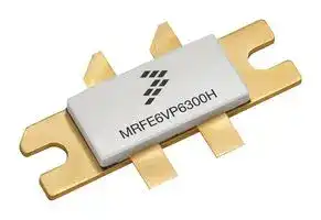


MRFE6VP100HR5
RF FET Transistor, 133 VDC, 1.8 MHz, 2000 MHz, NI-780
- Manufacturer: NXP
- Product type: RF FETs
- Drain Source Voltage Vds:133VDC; Continuous Drain Current Id:-; Power Dissipation Pd:-; Operating Frequency Min:1.8MHz; Operating Frequency Max:2000MHz; RF Transistor Case:NI-780; No. of
- MSL: -
- SVHC: No SVHC (27-Jun-2024)
- No. of Pins: 4Pins
- Channel Type: N Channel
- Product Range: -
- Power Dissipation: -
- Transistor Mounting: Flange
- Transistor Case Style: NI-780
- Operating Frequency Max: 2000MHz
- Operating Frequency Min: 1.8MHz
- Drain Source Voltage Vds: 133VDC
- Operating Temperature Max: 225°C
- Continuous Drain Current Id: -
| Delivery and price | |
|---|---|
| Units per pack | 10 |
| Price | 142.31 € |
| Current stock | 10+ |
| Lead time | 30 days |
**Freescale Semiconductor** Technical Data

Document Number: MRFE6VP100H Rev. 0, 5/2012

## **RF Power LDMOS Transistors** High Ruggedness N--Channel Enhancement--Mode Lateral MOSFETs

RF power transistors designed for both narrowband and broadband ISM, broadcast and aerospace applications operating at frequencies from 1.8 to 2000 MHz. These devices are fabricated using Freescale’s enhanced ruggedness platform and are suitable for use in applications where high VSWRs are encountered.

## **MRFE6VP100HR5 MRFE6VP100HSR5**

## **1.8--2000 MHz, 100 W, 50 V BROADBAND**

**Typical Performance:** VDD = 50 Volts **RF POWER LDMOS TRANSISTORS**

**Frequency Pout Gps** η **D IMD (MHz) Signal Type (W) (dB) (%) (dBc)** 30--512 **[(1,3)]** Two--Tone 100 PEP 19.0 30.0 --30 (100 kHz spacing) 512 **[(2)]** CW 100 27.2 70.0 — 512 **[(2)]** Pulse (200 μsec, 20% 100 Peak 26.0 70.0 — **NI--780--4** Duty Cycle) **MRFE6VP100HR5** ~~EE~~ S **Load Mismatch/Ruggedness Frequency Pout Test (MHz) Signal Type VSWR (W) Voltage Result** 512 **[(2)]** Pulse >65:1 130 50 No Device (100 μsec, 20% at all Phase (3 dB Degradation Duty Cycle) Angles Overdrive) **NI--780S--4 MRFE6VP100HSR5** 512 **[(2)]** CW 126 (3 dB Overdrive) ~~SS~~ 1. Measured in 30--512 MHz broadband reference circuit. 2. Measured in 512 MHz narrowband test circuit. 3. The values shown are the minimum measured performance numbers across the Gate A Drain A indicated frequency range.

**==> picture [155 x 107] intentionally omitted <==**

**----- Start of picture text -----**<br>
Gate A Drain A<br>Gate B Drain B<br>(Top View)<br>Note: The backside of the package is the<br>source terminal for the transistor.<br>**----- End of picture text -----**<br>


## **Features**

- Wide Operating Frequency Range

- Extremely Rugged

- Unmatched, Capable of Very Broadband Operation

- Integrated Stability Enhancements

- Low Thermal Resistance

- Integrated ESD Protection Circuitry

- In Tape and Reel. R5 Suffix = 50 Units, 56 mm Tape Width, 13 inch Reel.

**Figure 1. Pin Connections**

**Table 1. Maximum Ratings Rating Symbol Value Unit** Drain--Source Voltage VDSS --0.5, +133 Vdc Gate--Source Voltage VGS --6.0, +10 Vdc Storage Temperature Range Tstg --65 to +150 °C Case Operating Temperature TC --40 to +150 °C Operating Junction Temperature **[(4,5)]** TJ --40 to +225 °C ~~ee~~ 4. Continuous use at maximum temperature will affect MTTF. 5. MTTF calculator available at http://www.freescale.com/rf. Select Software & Tools/Development Tools/Calculators to access MTTF calculators by product.

© Freescale Semiconductor, Inc., 2012. All rights reserved.

**MRFE6VP100HR5 MRFE6VP100HSR5**

RF Device Data Freescale Semiconductor, Inc.

1

**Table 2. Thermal Characteristics**

|**Characteristic**<br>**Symbol**<br>**Value (1,2)**<br>**Unit**<br>Thermal Resistance, Junction to Case<br>CW: Case Temperature 81°C, 100 W CW, 50 Vdc, IDQ(A+B)= 100 mA, 512 MHz<br>RθJC<br>0.38<br>°C/W<br>Thermal Impedance, Junction to Case<br>Pulse: Case Temperature 73°C, 100 W Peak, 100μsec Pulse Width,<br>20% Duty Cycle, 50 Vdc, IDQ(A+B)= 100 mA, 512 MHz<br>ZθJC<br>0.12<br>°C/W<br>~~——e~~|
|---|
|**Table 3. ESD Protection Characteristics**|
|**Test Methodology**<br>**Class**<br>Human Body Model (per JESD22--A114)<br>2, passes 2500 V<br>Machine Model (per EIA/JESD22--A115)<br>B, passes 250 V<br>Charge Device Model (per JESD22--C101)<br>IV, passes 2000 V<br>**Table 4. Electrical Characteristics** (TA= 25°C unless otherwise noted)<br>**Characteristic**<br>**Symbol**<br>**Min**<br>**Typ**<br>**Max**<br>**Unit**<br>~~a~~|
|**Off Characteristics (3)**|
|Gate--Source Leakage Current<br>(VGS= 5 Vdc, VDS= 0 Vdc)<br>IGSS<br>—<br>—<br>400<br>nAdc<br>Drain--Source Breakdown Voltage<br>(VGS= 0 Vdc, ID= 50 mA)<br>V(BR)DSS<br>133<br>141<br>—<br>Vdc<br>Zero Gate Voltage Drain Leakage Current<br>(VDS= 50 Vdc, VGS= 0 Vdc)<br>IDSS<br>—<br>—<br>3<br>μAdc<br>Zero Gate Voltage Drain Leakage Current<br>(VDS= 100 Vdc, VGS= 0 Vdc)<br>IDSS<br>—<br>—<br>10<br>μAdc<br>**On Characteristics**<br>Gate Threshold Voltage **(3)**<br>(VDS= 10 Vdc, ID= 170μAdc)<br>VGS(th)<br>1.6<br>2.1<br>2.6<br>Vdc<br>Gate Quiescent Voltage<br>(VDD= 50 Vdc, ID= 100 mAdc, Measured in Functional Test)<br>VGS(Q)<br>2.1<br>2.6<br>3.1<br>Vdc<br>Drain--Source On--Voltage **(3)**<br>(VGS= 10 Vdc, ID= 1 Adc)<br>VDS(on)<br>—<br>0.23<br>—<br>Vdc<br>**Dynamic Characteristics (3)**<br>Reverse Transfer Capacitance<br>(VDS= 50 Vdc±30 mV(rms)ac @ 1 MHz, VGS= 0 Vdc)<br>Crss<br>—<br>0.24<br>—<br>pF<br>Output Capacitance<br>(VDS= 50 Vdc±30 mV(rms)ac @ 1 MHz, VGS= 0 Vdc)<br>Coss<br>—<br>23.9<br>—<br>pF<br>Input Capacitance<br>(VDS= 50 Vdc, VGS= 0 Vdc±30 mV(rms)ac @ 1 MHz)<br>Ciss<br>—<br>73.6<br>—<br>pF<br>~~SSeeeeeae~~<br>~~——$— EE~~<br>~~$F~~|
|**Functional Tests**(In Freescale Test Fixture, 50 ohm system) VDD= 50 Vdc, IDQ(A+B)= 100 mA, Pout= 100 W Peak (20 W Avg.), f = 512 MHz,|
|200μsec Pulse Width, 20% Duty Cycle|
|Power Gain<br>Gps<br>25.0<br>26.0<br>27.0<br>dB<br>Drain Efficiency<br>ηD<br>68.0<br>70.0<br>—<br>%<br>Input Return Loss<br>IRL<br>—<br>--14<br>--9<br>dB<br>~~—<——~~|
|**Load Mismatch/Ruggedness**(In Freescale Test Fixture, 50 ohm system, IDQ(A+B)= 100 mA)|
|**Frequency**<br>**(MHz)**<br>**Signal**<br>**Type**<br>**VSWR**<br>**Pout**<br>**(W)**<br>**Test Voltage, VDD**<br>**Result**<br>512<br>Pulse<br>(100μsec, 20% Duty Cycle)<br>>65:1<br>at all Phase Angles<br>130 Peak<br>(3 dB Overdrive)<br>50<br>No Device Degradation<br>CW<br>126<br>(3 dB Overdrive)<br>~~sa~~|
|1. MTTF calculator available athttp://www.freescale.com/rf<br>.Select Software & Tools/Development Tools/Calculators to access MTTF|
|calculators by product.|


2. Refer to AN1955, _Thermal Measurement Methodology of RF Power Amplifiers._ Go to http://www.freescale.com/rf. Select Documentation/Application Notes -- AN1955.

3. Each side of device measured separately.

**MRFE6VP100HR5 MRFE6VP100HSR5**

RF Device Data Freescale Semiconductor, Inc.

2

## **TYPICAL CHARACTERISTICS**

**==> picture [499 x 190] intentionally omitted <==**

**----- Start of picture text -----**<br>
1000 1.05<br>200 mA<br>Measured withVGS = 0 Vdc  ±30 mV(rms)ac @ 1 MHz 1.04 IDQ(A+B) = 100 mA VDD = 50 Vdc<br>100 Ciss 1.03 300 mA<br>1.02<br>a 1.01 600 mA ~<br>10 a Coss 1 Ne<br>0.99<br>0.98<br>1 e e a Sa<br>0.97<br>Crss<br>0.96<br>0.1 a 0.95 aeeee ee<br>0 10 20 30 40 50 --50 --25 0 25 50 75 100<br>VDS, DRAIN--SOURCE VOLTAGE (VOLTS) TC, CASE TEMPERATURE (°C)<br>Note:  Each side of device measured separately. Figure 3. Normalized VGS versus Quiescent  versus Quiescent<br>GS(Q)<br>NORMALIZED V<br>C, CAPACITANCE (pF)<br>**----- End of picture text -----**<br>


**Figure 3. Normalized VGS versus Quiescent Current and Case Temperature**

**Figure 2. Capacitance versus Drain--Source Voltage**

|**IDQ (mA)**|**Slope (mV/**°**C)**|
|---|---|
|100|--1.945|
|200|--1.826|
|300|--1.700|
|600|--1.648|


**==> picture [239 x 202] intentionally omitted <==**

**----- Start of picture text -----**<br>
10 [8]<br>==<br>ID = 2.2 Amps VDD = 50 Vdc<br>10 [7]<br>AN<br>HERR Eee<br>2.8 Amps<br>10 [6]<br>ao S SR<br>SSS 3.3 Amps SSRES<br>e e<br>10 [5]<br>QO ESSee ee ee<br>a<br>10 [4] PEEP EPErP Pere ere et ft<br>90 110 130 150 170 190 210 230 250<br>TJ, JUNCTION TEMPERATURE (°C)<br>Note:  MTTF value represents the total cumulative operating time<br>under indicated test conditions.<br>MTTF (HOURS)<br>**----- End of picture text -----**<br>


**Figure 4. MTTF versus Junction Temperature -- CW**

**MRFE6VP100HR5 MRFE6VP100HSR5**

RF Device Data Freescale Semiconductor, Inc.

3

## **512 MHz NARROWBAND PRODUCTION TEST FIXTURE**

**==> picture [465 x 248] intentionally omitted <==**

**----- Start of picture text -----**<br>
MRFE6VP100H/S ———F<br>B1 ° Rev. 1 C10 C11 C12<br>eT : C2 ITAnn<br>° 0000 of bBOO000000000000000<br>C1<br>OnX o| tES ° ° C13 ° pp C14 4) ®<br>3] ° St Lp<br>0 o\oo °} e00000 == °°<br>COAX1 L1 °8 °000000 L3 =y |°8 COAX3<br>O° oO<br>° eo00000 °<br>° fe}<br>2000 000000000<br>= o<br>=® | C4 C6 C15 C24<br>®& C16 H | oo0 o00 0<br>8 Boe ml )<br>® Foo C7 C17 ws 4 —_|<br>oO ein LI |<br>i) C5 C18 ll 000000<br>an C3<br>wey ®<br>"4 o000 900000000<br>rs °<br>° So0000|<br>° COAX2 L2 olooofo°6 ° 000000 ° °° 000000 L4 | =EY =] 163°°jolo COAX4<br>fo} ° O°<br>C19<br>C8 Oo| F= ) meee HT° b C20 © ©<br>° e000 Q booo00000» 190000<br>POO0O0000000 ° C9 LCL —i‘(CiC<br>| B2 [le C21 C22 C23<br>CUT OUT AREA<br>**----- End of picture text -----**<br>


**Figure 5. MRFE6VP100HR5(HSR5) Narrowband Test Circuit Component Layout — 512 MHz**

**Table 5. MRFE6VP100HR5(HSR5) Narrowband Test Circuit Component Designations and Values — 512 MHz**

|**Part**|**Description**|**Part Number**|**Manufacturer**|
|---|---|---|---|
|B1, B2|Small Ferrite Beads, Surface Mount|2743019447|Fair-Rite|
|C1, C8|22μF, 35 V Tantalum Capacitors|T491X226K035AT|Kemet|
|C2, C9|120 pF Chip Capacitors|ATC100B121JT500XT|ATC|
|C3|4.3 pF Chip Capacitor|ATC100B4R3CT500XT|ATC|
|C4, C5|56 pF Chip Capacitors|ATC100B560CT500XT|ATC|
|C6, C7, C15, C16, C17, C18|27 pF Chip Capacitors|ATC100B270JT500XT|ATC|
|C10, C21|0.1μF Chip Capacitors|C1812F104K1RACTU|Kemet|
|C11, C22|0.01μF Chip Capacitors|C1825C103K1GACTU|Kemet|
|C12, C23|470μF, 63 V Electrolytic Capacitors|MCGPR63V477M13X26-RH|Multicomp|
|C13, C19|240 pF Chip Capacitors|ATC100B241JT200XT|ATC|
|C14, C20|2.2μF Chip Capacitors|G2225X7R225KT3AB|ATC|
|C24|7.5 pF Chip Capacitor|ATC100B7R5CT500XT|ATC|
|Coax1, 2|25ΩSemi Rigid Coax, 2.2″Shield Length|UT-141C-25|Micro-Coax|
|Coax3, 4|25ΩSemi Rigid Coax, 2.0″Shield Length|UT-141C-25|Micro-Coax|
|L1, L2|5 Turns, 18.5 nH Inductors, Wire Wound|A05TKLC|Coilcraft|
|L3, L4|7 Turns, 22 nH Inductors, Wire Wound|B07TJLC|Coilcraft|
|PCB|0.030″,εr= 2.55|AD255D|Arlon|


**MRFE6VP100HR5 MRFE6VP100HSR5**

RF Device Data Freescale Semiconductor, Inc.

4

**==> picture [340 x 583] intentionally omitted <==**

**----- Start of picture text -----**<br>
[!<br>Fh<br>C ir C i<br>eal eal<br>meal 4h<br>[H1! [H!<br>Fh Eh<br>| i<br>==<br>| I a<br>| i<br>= =<br>t i | | m o LU<br>° i] i] S<br>e al H 4h<br>| i<br>RF<br>OUTPUT<br>Z14<br>C24<br>Z13<br>SUPPLY SUPPLY<br>V V<br>+ C12 COAX3 COAX4 + C23<br>C11 C22<br>C10 C21<br>Z12 Z25<br>C14 C20<br>C15 C16 C17 C18<br>C13 C19<br>L3 Z10 Z11 Z24 Z23 L4<br>Z9 Z22<br>DUT<br>L1 Z7 Z8 Z21 Z20 L2<br>C2 Z6 Z19 C9<br>C7<br>B1 B2<br>Z5 Z18<br>+ C1 C6 + C8<br>Z4 Z17<br>BIAS C4 C5 BIAS<br>V V<br>Z3 Z16<br>C3<br>Z2 Z15<br>Figure 6. MRFE6VP100HR5(HSR5) Narrowband Test Circuit Schematic — 512 MHz<br>COAX1 COAX2<br>Z1<br>RF<br>INPUT<br>**----- End of picture text -----**<br>


|**Figure 6. MRFE6VP100HR5(HSR5) Narrowband Test Circuit Schematic — 512 MHz**<br>~~==~~|**Table 6. MRFE6VP100HR5(HSR5) Narrowband Test Circuit Microstrips — 512 MHz**|**Description**<br>**Microstrip**<br>**Description**<br>**Microstrip**|Z1<br>0.366″ ×0.082″Microstrip<br>Z9, Z22<br>0.271″ ×0.507″Microstrip|Z2, Z15<br>0.070″ ×0.102″Microstrip<br>Z10*, Z23*<br>0.822″ ×0.150″Microstrip|Z3, Z16<br>0.094″ ×0.102″Microstrip<br>Z11, Z24<br>0.590″ ×0.216″Microstrip|Z4, Z17<br>0.103″ ×0.102″Microstrip<br>Z12, Z25<br>0.257″ ×0.216″Microstrip|Z5, Z18<br>0.125″ ×0.102″Microstrip<br>Z13<br>0.192″ ×0.082″Microstrip|Z6, Z19<br>0.168″ ×0.102″Microstrip<br>Z14<br>0.173″ ×0.082″Microstrip|Z7*, Z20*<br>0.912″ ×0.058″Microstrip<br>* Line length includes microstrip bends|Z8, Z21<br>0.420″ ×0.726″Microstrip|
|---|---|---|---|---|---|---|---|---|---|---|


**MRFE6VP100HR5 MRFE6VP100HSR5**

RF Device Data Freescale Semiconductor, Inc.

5

## **TYPICAL CHARACTERISTICS — 512 MHz**

**==> picture [500 x 457] intentionally omitted <==**

**----- Start of picture text -----**<br>
135 58<br>120 VDD = 50 Vdc P| | | t o 56 VDD = 50 Vdc | | ft |<br>f = 512 MHz 54 IDQ(A+B) = 100 mA<br>105<br>52 f = 512 MHz<br>90 pP| |S| | YlAAa e 50 pSa<br>75 ey Pin = 0.24 W Pin = 0.12 W 48 — 2a<br>46<br>60 e e ey e e<br>44<br>45 P| | | sf 2 I | 42 7A<br>40<br>30<br>38<br>15<br>36<br>POOR «= EERE<br>0 A> aa 34 od<br>0 0.5 1 1.5 2 2.5 3 3.5 4 4.5 12 14 16 18 20 22 24 26 28 30<br>VGS, GATE--SOURCE VOLTAGE (VOLTS) Pin, INPUT POWER (dBm)<br>Figure 7. CW Output Power versus Gate--Source<br>Voltage at a Constant Input Power f P1dB P3dB<br>(MHz) (W) (W)<br>512 117 132<br>Figure 8. CW Output Power versus Input Power<br>28 80<br>VDD = 50 Vdc --30 _ C<br>27 If = 512 MHzDQ(A+B) = 100 mA 25 _ C 70<br>26 85 _ C 60<br>25 og | 50<br>S TC = --30 _ C EI"ann \\<br>24 40<br>ZA 25 _ C<br>23 Gps 30<br>S 85 _ C H ηD<br>22 20<br>Pe a<br>21 aT EE ELL 10<br>3 10 100 200<br>Pout, OUTPUT POWER (WATTS) CW<br>, OUTPUT POWER (WATTS) , OUTPUT POWER (dBm)<br>out out<br>P P<br>, POWER GAIN (dB)<br>ps  DRAIN EFFICIENCY (%)<br>G D,<br>η<br>**----- End of picture text -----**<br>


**Figure 9. Power Gain and Drain Efficiency versus CW Output Power**

**MRFE6VP100HR5 MRFE6VP100HSR5**

RF Device Data Freescale Semiconductor, Inc.

6

## **512 MHz NARROWBAND PRODUCTION TEST FIXTURE**

**==> picture [308 x 182] intentionally omitted <==**

**----- Start of picture text -----**<br>
VDD = 50 Vdc, IDQ(A+B) = 100 mA, Pout = 100 W Peak<br>f Zsource Zload<br>MHz Ω Ω<br>512 1.50 + j8.90 12.2 + j18.0<br>| Zsource = Test circuit impedance as measured from |_|]<br>gate to gate, balanced configuration.<br>Zload = Test circuit impedance as measured from<br>drain to drain, balanced configuration.<br>Input Device Output<br>Matching + Under -- Matching<br>50 Ω Network Test Network 50 Ω<br>Lit -- t + l<br>h<br>Zsource Zload<br>**----- End of picture text -----**<br>


**Figure 10. Narrowband Series Equivalent Source and Load Impedance — 512 MHz**

**MRFE6VP100HR5 MRFE6VP100HSR5**

RF Device Data Freescale Semiconductor, Inc.

7

## **30--512 MHz BROADBAND REFERENCE CIRCUIT**

**Table 7. 30--512 MHz Broadband Performance** (In Freescale Reference Circuit, 50 ohm system) VDD = 50 Volts, IDQ(A+B) = 400 mA

|**Signal Type**<br>~~a~~|**Pout**<br>**(W)**<br>~~ee~~|**f**<br>**(MHz)**<br>~~ee~~|**Gps**<br>**(dB)**<br>~~ee~~|η**D**<br>**(%)**<br>~~ee~~|**IMD**<br>**(dBc)**|
|---|---|---|---|---|---|
|Two-Tone<br>(200 kHz spacing)<br>~~a~~|25 PEP<br>~~ee ~~<br>~~SS~~|30<br> ~~ee~~<br>~~a~~<br>~~SS~~|24.5<br>~~ee ~~<br>~~a~~<br>~~SS~~|25.3<br> ~~ee~~<br>~~a~~<br>~~SS~~|-37.8<br>~~a~~<br>~~SS~~|
|||100<br>~~SS~~|19.6<br>~~SS~~|19.9<br>~~SS~~|-35.7<br>~~SS~~|
|||512<br>~~SS~~<br>~~a~~|21.3<br>~~SS~~<br>~~a~~<br>~~a~~|20.3<br>~~SS~~<br>~~a~~<br>~~a~~|-42.8<br>~~SS~~<br>~~a~~<br>~~a~~|
||50 PEP|30<br>~~a~~|24.5<br>~~a~~<br>~~a~~|36.7<br>~~a~~<br>~~a~~|-29.1<br>~~a~~<br>~~a~~|
|||100<br>~~a~~|19.9<br>~~a~~|28.9<br>~~a~~|-32.9<br>~~a~~|
|||512<br>~~a~~|21.7<br>~~a~~<br>~~a~~|29.6<br>~~a~~<br>~~a~~|-43.7<br>~~a~~<br>~~a~~|
||75 PEP|30<br>~~a~~|23.9<br>~~a~~<br>~~a~~|44.6<br>~~a~~<br>~~a~~|-24.1<br>~~a~~<br>~~a~~|
|||100<br>~~a~~<br>~~a~~|19.4<br>~~a~~<br>~~a~~<br>~~a~~|35.1<br>~~a~~<br>~~a~~<br>~~a~~|-25.1<br>~~a~~<br>~~a~~<br>~~a~~|
|||512<br>~~a~~<br>~~a~~|21.7<br>~~a~~<br>~~a~~|36.8<br>~~a~~<br>~~a~~|-37.4<br>~~a~~<br>~~a~~|
||100 PEP|30<br>~~a~~|23.2<br>~~a~~<br>~~a~~|50.7<br>~~a~~|-20.1<br>~~a~~|
|||100<br>~~a~~|18.8<br>~~a~~<br>~~a~~|39.8<br>~~a~~<br>~~a~~|-20.4<br>~~a~~<br>~~a~~|
|||512<br>~~a~~<br>~~a~~|21.6<br>~~a~~<br>~~a~~<br>~~a~~<br>~~a~~|42.2<br>~~a~~<br>~~a~~<br>~~a~~<br>~~a~~|-28.6<br>~~a~~<br>~~a~~<br>~~a~~|


**MRFE6VP100HR5 MRFE6VP100HSR5**

RF Device Data Freescale Semiconductor, Inc.

8

## **30--512 MHz BROADBAND REFERENCE CIRCUIT**

**==> picture [339 x 284] intentionally omitted <==**

**----- Start of picture text -----**<br>
E—} |} 6<br>R1 C1 MRFE6VP100H C6 C5 C14<br>O°° Rev. 1 [#— \<br>6 |<br>o] |_| |oooo 6 | Ey 000000000000000<br>@ oi6 PEs °° E6 ‘mnp T4<br>R3 0000 fo)6 oo Ppb (><br>° ° AA Lo<br>T2 s 000000 L1 [| 8<br>Connects shields aa }° E5<br>above PCB oo00000°<br>fe}<br>E3 fe}8<br>reescalev u °0000000000<br>C2 \ C7<br>| \| || > C8 LI<br>on Ne | LU Q1 imi= f}<br>E1<br>E2 C9<br>i | Hine<br>C3 C10<br>0000000000 C11 C15<br>E4 °3°<br>)5<br>)°<br>000000<br>T3 )ay, L2 }°<br>0 °<br>o000S. Q00000° HOUS AY °LL<br>° 0° O<br>T1 OFA fo)°>| IB—]J )°Ke.0.0 R4 0 ° °° E7 Qgigini abbDF>000000000000000<br>R2 I) C4 5° C12 C13 = y C16<br>**----- End of picture text -----**<br>


**Figure 11. MRFE6VP100HR5(HSR5) Broadband Reference Circuit Component Layout — 30--512 MHz**

**Table 8. MRFE6VP100HR5(HSR5) Broadband Reference Circuit Component Designations and Values — 30--512 MHz**

|**Part**|**Description**|**Part Number**|**Manufacturer**|
|---|---|---|---|
|C1, C4|2.2μF Chip Capacitors|C1825C225J5RAC|Kemet|
|C2, C3, C7, C8, C9, C10|C2, C3, C7, C8, C9, C10<br>20K pF Chip Capacitors|ATC200B203KT50XT|ATC|
|C5, C13|200 nF Chip Capacitors|C1812C224K5RAC-TU|Kemet|
|C6, C12|2.2μF Chip Capacitors|G2225X7R225KT3AB|ATC|
|C11|2.7 pF Chip Capacitor|ATC100B2R7BT500XT|ATC|
|C14, C16|470μF, 63 V Electrolytic Capacitors|MCGPR63V477M13X26-RH|Multicomp|
|C15|2.0 pF Chip Capacitor|ATC100B2R0BT500XT|ATC|
|E1, E2|#43 Ferrite Beads|2643023402|Fair-Rite|
|E3, E4, E5|Binocular Toroid K Material|12-365-K|Ferronics|
|E6, E7|Toroid Ferrite K Material|11--750--K|Ferronics|
|L1, L2|10 Turns, #18 AWG, Toroid Transformer with<br>Ferrites E6, E7|8075 Copper Magnetic Wire|Belden|
|Q1|RF Power LDMOS Transistor|MRFE6VP100HR5|Freescale|
|R1, R2|10Ω, 1/4 W Chip Resistors|CRCW120610ROJNEA|Vishay|
|R3, R4|56Ω, 1/4 W Chip Resistors|CRCW120656ROJNEA|Vishay|
|T1|50ΩFlex Cable, 4″|Sucoform 141|Hubert+Suhner|
|T2, T3|22ΩFlex Cable, 3.25″|M27500-16RC1509|Whitmor-Wirenetics|
|T4|25ΩSemi Rigid, 2.75″|UT-90-25|Micro-Coax|
|PCB|0.030″,εr = 2.55|AD255A|Arlon|


**MRFE6VP100HR5 MRFE6VP100HSR5**

RF Device Data Freescale Semiconductor, Inc.

9

**==> picture [496 x 292] intentionally omitted <==**

**----- Start of picture text -----**<br>
+ VSUPPLY<br>R1<br>VBIAS L1, E6 C6 C5 C14<br>C1 R3<br>Z12 C7<br>Z6 Z10 Z14 Z16 Z18<br>Z2 Z4 Z8 C8<br>RF T3<br>INPUT<br>Z1 T1 C2 E4 T4 RF<br>+ Le a n<br>OUTPUT<br>DUT Z20<br>E1, E2 C11 E5<br>Z3 Z5 Z9<br>T2<br>C15<br>C3 E3 Z11 Z15 C9 Z17 Z19<br>Z7<br>Z13<br>C10<br>R4<br>R2 L2, E7<br>VBIAS<br>C4 + VSUPPLY<br>C12 C13 C16<br>° FH<br>**----- End of picture text -----**<br>


**Figure 12. MRFE6VP100HR5(HSR5) Broadband Test Circuit Schematic — 30--512 MHz**

**Table 9. MRFE6VP100HR5(HSR5) Narrowband Test Circuit Microstrips — 30--512 MHz**

|**Microstrip**|**Description**|Z12*, Z13*<br>1.125″ ×0.150″Microstrip<br>Z14, Z15<br>0.563″ ×0.219″Microstrip<br>Z16, Z17<br>0.094″ ×0.219″Microstrip<br>Z18, Z19<br>0.156″ ×0.219″Microstrip<br>Z20<br>0.359″ ×0.078″Microstrip<br>* Line length includes microstrip bends<br>**Description**<br>**Microstrip**|**Microstrip**|**Description**|
|---|---|---|---|---|
|Z1|0.366″ ×0.082″Microstrip||Z12*, Z13*|1.125″ ×0.150″Microstrip|
|Z2, Z3|0.070″ ×0.102″Microstrip||Z14, Z15|0.563″ ×0.219″Microstrip|
|Z4,Z5|0.094″ ×0.102″Microstrip||Z16, Z17|0.094″ ×0.219″Microstrip|
|Z6*, Z7*|1.375″ ×0.063″Microstrip||Z18, Z19|0.156″ ×0.219″Microstrip|
|Z8, Z9|0.561″ ×0.219″Microstrip||Z20|0.359″ ×0.078″Microstrip|
|Z10, Z11|0.250″ ×0.219″Microstrip||||


**MRFE6VP100HR5 MRFE6VP100HSR5**

RF Device Data Freescale Semiconductor, Inc.

10

## **TYPICAL CHARACTERISTICS — 30--512 MHz BROADBAND REFERENCE CIRCUIT**

**==> picture [275 x 174] intentionally omitted <==**

**----- Start of picture text -----**<br>
28 210<br>26 VDD = 50 Vdc, Pin = 2 W 195<br>24 IDQ(A+B) = 100 mA 180<br>22 165<br>20 150<br>18 Pout 135<br>16 120<br>14 RS SR R  R EE 105<br>12 Gps 90<br>10 75<br>8 So n n aee a e 60<br>6 ηD 45<br>4 p S e r 30<br>2 15<br>0 pS 0<br>0 50 100 150 200 250 300 350 400 450 500 550<br>f, FREQUENCY (MHz)<br>, POWER GAIN (dB)<br>ps<br>G , DRAIN EFFICIENCY (%)D<br>, OUTPUT POWER (WATTS) CW η<br>out<br>P<br>**----- End of picture text -----**<br>


**Figure 13. Power Gain, CW Output Power and Drain Efficiency versus Frequency at a Constant Input Power**

**==> picture [500 x 201] intentionally omitted <==**

**----- Start of picture text -----**<br>
200 200<br>VDD = 50 Vdc VDD = 50 Vdc 30 MHz<br>Pin = 1 W 30 MHz Pin = 2 W<br>150 150<br>Ppoiil aA ; |<br>512 MHz<br>100 100<br>Gf 512 MHz 100 MHz tthg 100 MHz<br>50 50<br>ff | LL<br>0 ee 0<br>0 0.5 1 1.5 2 2.5 3 3.5 4 0 0.5 1 1.5 2 2.5 3 3.5 4<br>VGS, GATE--SOURCE VOLTAGE (VOLTS) VGS, GATE--SOURCE VOLTAGE (VOLTS)<br>Figure 14. CW Output Power versus Gate--Source Figure 15. CW Output Power versus Gate--Source<br>Voltage at a Constant Input Power Voltage at a Constant Input Power<br>, OUTPUT POWER (WATTS) , OUTPUT POWER (WATTS)<br>out out<br>P P<br>**----- End of picture text -----**<br>


**MRFE6VP100HR5 MRFE6VP100HSR5**

RF Device Data Freescale Semiconductor, Inc.

11

**TYPICAL CHARACTERISTICS — 30--512 MHz BROADBAND REFERENCE CIRCUIT**

**==> picture [234 x 251] intentionally omitted <==**

**----- Start of picture text -----**<br>
52<br>VDD = 50 Vdc<br>50<br>IDQ(A+B) = 100 mA<br>48 E e<br>46 f = 30 MHz<br>44 — SPYeT<br>42 | YKhY)<br>| | i |<br>512 MHz<br>40<br>38 tAA A |,| |<br>100 MHz<br>36<br>| | | |<br>34 | otYY,| ct| | ET| | | | |<br>18 20 22 24 26 28 30 32 34 36<br>Pin, INPUT POWER (dBm)<br>f P1dB P3dB<br>(MHz) (W) (W)<br>30 78 107<br>100 81 118<br>512 123 142<br>, OUTPUT POWER (dBm)<br>out<br>P<br>**----- End of picture text -----**<br>


**Figure 16. CW Output Power versus Input Power**

**==> picture [254 x 175] intentionally omitted <==**

**----- Start of picture text -----**<br>
26 80<br>VDD = 50 Vdc<br>24 IDQ(A+B) = 100 mA 70<br>30 MHz ηD<br>22 60<br>an)a e<br>20 512 MHz 50<br>18 se S re e ” eo 40<br>100 MHz  <(\\u Gps<br>16 30<br>512 MHz<br>100 MHz<br>14 gn 20<br>30 MHz<br>12 TA coer) TTT 10<br>3 10 100 — 200<br>Pout, OUTPUT POWER (WATTS) CW<br>, POWER GAIN (dB)<br>ps  DRAIN EFFICIENCY (%)<br>G D,<br>η<br>**----- End of picture text -----**<br>


**Figure 17. Power Gain and Drain Efficiency versus CW Output Power**

**MRFE6VP100HR5 MRFE6VP100HSR5**

RF Device Data Freescale Semiconductor, Inc.

12

## **TYPICAL CHARACTERISTICS — 30--512 MHz BROADBAND REFERENCE CIRCUIT — TWO--TONE[(1)]**

**==> picture [500 x 175] intentionally omitted <==**

**----- Start of picture text -----**<br>
--10 --10<br>VDD = 50 Vdc, IDQ(A+B) = 400 mA VDD = 50 Vdc, IDQ(A+B) = 400 mA<br>--20 f1 = 29.9 MHz, f2 = 30.1 MHz ELLIE --20 f1 = 99.9 MHz, f2 = 100.1 MHz TULLE<br>Two--Tone Measurements Two--Tone Measurements<br>--30 --30<br>TM ne<br>--40 --40 3rd Order<br>3rd Order<br>--50 --50<br>THI L l J Y ,<br>5th Order<br>5th Order<br>--60 --60<br>et 7th Order ATI e24 0 ||<br>7th Order<br>--70 im i --70 aa aie<br>1 10 100 200 1 10 100 200<br>Pout, OUTPUT POWER (WATTS) PEP Pout, OUTPUT POWER (WATTS) PEP<br>IMD, INTERMODULATION DISTORTION (dBc) IMD, INTERMODULATION DISTORTION (dBc)<br>**----- End of picture text -----**<br>


**Figure 18. Intermodulation Distortion Products versus Output Power — 30 MHz**

**Figure 19. Intermodulation Distortion Products versus Output Power — 100 MHz**

**==> picture [238 x 201] intentionally omitted <==**

**----- Start of picture text -----**<br>
--20<br>VDD = 50 Vdc, IDQ(A+B) = 400 mA<br>--30 f1 = 511.9 MHz, f2 = 512.1 MHz<br>Two--Tone Measurements<br>--40 Fan THB<br>3rd Order =  f<br>--50<br>5th Order<br>--60 SLT 7th Order<br>--70 S e l t<br>1 10 100 200<br>Pout, OUTPUT POWER (WATTS) PEP<br>Figure 20. Intermodulation Distortion<br>Products versus Output Power — 520 MHz<br>IMD, INTERMODULATION DISTORTION (dBc)<br>**----- End of picture text -----**<br>


1. The distortion products are referenced to one of the two tones and the peak envelope power (PEP) is 6 dB above the power in a single tone.

**MRFE6VP100HR5 MRFE6VP100HSR5**

RF Device Data Freescale Semiconductor, Inc.

13

**==> picture [385 x 596] intentionally omitted <==**

**----- Start of picture text -----**<br>
30--512 MHz BROADBAND REFERENCE CIRCUIT<br>G anes<br>IY) Lob SSSS e<br>we, YQ ?,<br>Zo = 50 Ω <><br>i> hfs e f = 512 MHz e<br>eh ee S es ZEROS<br>sis Gf eae taten ee n  a LEE RRS<br>sf Ie) f = 512 MHz fea! é Ly LEE IPR TEES PLP REE<br>ef /s i aa Zsource Pee Eke wees ae PRIS<br>elef, ee e ee L et es wae,<br>fe] As yA EEEEEE Scenes<br>ates<br>dle] celeFH CENes Aee eeeUae eaeeirer COMPONENT  meee<br>mae<br>f = 30 MHz f = 30 MHz<br>ee eeeembcast<br>aT ic e Seu aeldieeen el CES<br>Zload . ae| oe<br>il Pee a tN ane ES S<br>ee ae SS R<br>2 Perish cence CNG RE ASRS SSSR SRS<br>2\2 Nol l ~ S SS Seis<br>stel2\"\.¥\"  Fie ( oo — Seeeasets S S ee SR |<br>® te Voi Pe A ES SSSR CAE<br>SOS ae, Ty ATH<br>A?ela | aSSey 5 SESSSSS, SOS SOSLRQY LOKI 9 LTATE<br>8) A RRS Ky SSSR KS eee ey, aaaee 7<br>ana\¢<> RAENfo)SSSWL3 G NesceWPRACSESSSERESeseenrcarrrenns» EREDSOK © ATPEE<br>VDD = 50 Vdc, Pout = 100 W CW<br>f Zsource Zload<br>MHz Ω Ω<br>30 10.7 + j1.20 45.8 – j9.00<br>64 10.9 + j0.70 39.7 – j15.4<br>88 10.9 + j0.50 33.9 – j18.1<br>108 10.3 + j0.70 30.0 – j14.4<br>144 11.0 + j0.70 26.0 – j16.7<br>170 10.4 + j0.60 21.8 – j13.4<br>230 9.90 + j0.90 17.0 – j10.7<br>352 8.90 + j2.30 13.8 – j0.60<br>450 7.60 + j4.80 16.9 + j9.50<br>512 7.20 + j6.00 23.7 + j13.5<br>Zsource = Test circuit impedance as measured from<br>gate to gate, balanced configuration.<br>Zload = Test circuit impedance as measured from<br>drain to drain, balanced configuration.<br>Input Device Output<br>Matching + Under -- Matching<br>50 Ω Network Test Network 50 Ω<br>-- +<br>Zsource Zload<br>**----- End of picture text -----**<br>


**Figure 21. Broadband Series Equivalent Source and Load Impedance — 30--512 MHz**

**MRFE6VP100HR5 MRFE6VP100HSR5**

RF Device Data Freescale Semiconductor, Inc.

14

**PACKAGE DIMENSIONS**

**MRFE6VP100HR5 MRFE6VP100HSR5**

RF Device Data Freescale Semiconductor, Inc.

15

**MRFE6VP100HR5 MRFE6VP100HSR5**

RF Device Data Freescale Semiconductor, Inc.

16

**MRFE6VP100HR5 MRFE6VP100HSR5**

RF Device Data Freescale Semiconductor, Inc.

17

**MRFE6VP100HR5 MRFE6VP100HSR5**

RF Device Data Freescale Semiconductor, Inc.

18

## **PRODUCT DOCUMENTATION, SOFTWARE AND TOOLS**

Refer to the following documents, software and tools to aid your design process.

## **Application Notes**

- AN1955: Thermal Measurement Methodology of RF Power Amplifiers

## **Engineering Bulletins**

- EB212: Using Data Sheet Impedances for RF LDMOS Devices

## **Software**

- Electromigration MTTF Calculator

- RF High Power Model

- .s2p File

## **Development Tools**

- Printed Circuit Boards

For Software and Tools, do a Part Number search at http://www.freescale.com, and select the “Part Number” link. Go to the Software & Tools tab on the part’s Product Summary page to download the respective tool.

## **REVISION HISTORY**

The following table summarizes revisions to this document.

**Revision Date Description** 0 May 2012 • Initial Release of Data Sheet ~~eT~~

**MRFE6VP100HR5 MRFE6VP100HSR5**

RF Device Data Freescale Semiconductor, Inc.

19

## _**How to Reach Us:**_

**Home Page:** freescale.com

**Web Support:** freescale.com/support

Information in this document is provided solely to enable system and software implementers to use Freescale products. There are no express or implied copyright licenses granted hereunder to design or fabricate any integrated circuits based on the information in this document.

Freescale reserves the right to make changes without further notice to any products herein. Freescale makes no warranty, representation, or guarantee regarding the suitability of its products for any particular purpose, nor does Freescale assume any liability arising out of the application or use of any product or circuit, and specifically disclaims any and all liability, including without limitation consequential or incidental damages. “Typical” parameters that may be provided in Freescale data sheets and/or specifications can and do vary in different applications, and actual performance may vary over time. All operating parameters, including “typicals,” must be validated for each customer application by customer’s technical experts. Freescale does not convey any license under its patent rights nor the rights of others. Freescale sells products pursuant to standard terms and conditions of sale, which can be found at the following address: http://www.reg.net/v2/webservices/Freescale/Docs/TermsandConditions.htm.

Freescale, the Freescale logo, AltiVec, C--5, CodeTest, CodeWarrior, ColdFire, C--Ware, Energy Efficient Solutions logo, Kinetis, mobileGT, PowerQUICC, Processor Expert, QorIQ, Qorivva, StarCore, Symphony, and VortiQa are trademarks of Freescale Semiconductor, Inc., Reg. U.S. Pat. & Tm. Off. Airfast, BeeKit, BeeStack, ColdFire+, CoreNet, Flexis, MagniV, MXC, Platform in a Package, QorIQ Qonverge, QUICC Engine, Ready Play, SafeAssure, SMARTMOS, TurboLink, Vybrid, and Xtrinsic are trademarks of Freescale Semiconductor, Inc. All other product or service names are the property of their respective owners. E 2012 Freescale Semiconductor, Inc.

**MRFE6VP100HR5 MRFE6VP100HSR5**

RF Device Data Freescale Semiconductor, Inc.

Document Number: MRFE6VP100H 20Rev. 0, 5/2012
Updated at April 10, 2026
NXP Semiconductors is a global leader in secure connectivity solutions, driving innovation across the automotive, industrial, IoT, mobile, and communications infrastructure markets. By developing advanced, purpose-built technologies, NXP enables devices to sense, think, connect, and act intelligently, delivering rigorously tested components that make the connected world safer and more efficient. Within the semiconductor space, NXP is highly regarded for its extensive range of high-performance integrated circuits and discrete devices. The brand's portfolio excels in drivers and interfaces, featuring a comprehensive selection of I/O expanders designed to streamline complex system architectures. For demanding high-frequency and wireless applications, NXP provides industry-leading RF FETs and RF/PIN diodes engineered to deliver exceptional signal integrity, efficiency, and reliability. The NXP product lineup further extends to essential discrete components, including versatile bipolar transistors, JFETs, and small signal diodes optimized for precision switching and amplification. Additionally, the portfolio supports advanced automation and smart applications with precision IC sensors, such as MEMS accelerometers, alongside specialized power management solutions like AC/DC LED driver ICs and single MOSFETs for cutting-edge electronics design.
About Novapart
Novapart is a B2B electronic component broker specialising in stock shortages and cost reduction. We source hard-to-find parts and identify compliant alternatives across a catalogue of 410,000+ components from 500+ manufacturers.
Learn more →Stock Shortage Specialist
When a component is unavailable, discontinued or has an unacceptable lead time, we tap into our network of vetted European and Asian distributors to source what you need — without compromising on quality or traceability.
Request a quote →Compliant Alternatives
We identify pin-to-pin, electrically equivalent substitutes that meet the same certifications (RoHS, AEC-Q100, REACH) as your original specification — validated against datasheets, not just part numbers. Often at a lower cost.
BOM Analysis service →