


MRF6V12250HR5
RF FET Transistor, 100 VDC, 960 MHz, 1215 MHz, NI-780
- Manufacturer: NXP
- Product type: RF FETs
- Channel Type: N Channel
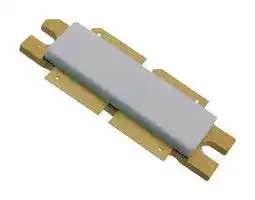
- Transistor Mounting: Flange
- Transistor Case Style: NI-780
| Delivery and price | |
|---|---|
| Units per pack | 5 |
| Price | 418.33 € |
| Current stock | 10+ |
| Lead time | 30 days |
**Freescale Semiconductor**

Document Number: MRF6V12250H Rev. 2, 4/2010

Technical Data

## **RF Power Field Effect Transistors**

## N--Channel Enhancement--Mode Lateral MOSFETs

RF Power transistors designed for applications operating at frequencies between 960 and 1215 MHz. These devices are suitable for use in pulsed applications.

- Typical Pulsed Performance: VDD = 50 Volts, IDQ = 100 mA, Pout = 275 Watts Peak (27.5 Watts Avg.), f = 1030 MHz, Pulse Width = 128 μsec, Duty Cycle = 10% Power Gain — 20.3 dB Drain Efficiency — 65.5%

## **MRF6V12250HR3 MRF6V12250HSR3**

**960--1215 MHz, 275 W, 50 V PULSED LATERAL N--CHANNEL RF POWER MOSFETs**

- Capable of Handling 10:1 VSWR, @ 50 Vdc, 1030 MHz, 275 Watts Peak Power

- Typical Broadband Performance: VDD = 50 Volts, IDQ = 100 mA, Pout = 250 Watts Peak (25 Watts Avg.), f = 960--1215 MHz, Pulse Width = 128 μsec, Duty Cycle = 10% Power Gain — 19.8 dB Drain Efficiency — 58%

## **Features**

- Characterized with Series Equivalent Large--Signal Impedance Parameters

- Internally Matched for Ease of Use

- Qualified Up to a Maximum of 50 VDD Operation

- Integrated ESD Protection

- Greater Negative Gate--Source Voltage Range for Improved Class C Operation

- RoHS Compliant

**==> picture [101 x 111] intentionally omitted <==**

**----- Start of picture text -----**<br>
CASE 465--06, STYLE 1<br>NI--780<br>MRF6V12250HR3<br>CASE 465A--06, STYLE 1<br>NI--780S<br>MRF6V12250HSR3<br>**----- End of picture text -----**<br>


- In Tape and Reel. R3 Suffix = 250 Units per 56 mm, 13 inch Reel.

## **Table 1. Maximum Ratings**

|**Table 1. Maximum Ratings**||||
|---|---|---|---|
|**Rating**|**Symbol**|**Value**|**Unit**|
|Drain--Source Voltage|VDSS|--0.5, +100|Vdc|
|Gate--Source Voltage|VGS|--6.0, +10|Vdc|
|Storage Temperature Range|Tstg|-- 65 to +150|°C|
|Case Operating Temperature|TC|150|°C|
|Operating Junction Temperature **(1,2)**|TJ|225|°C|
|**Table 2. Thermal Characteristics**||||
|**Characteristic**|**Symbol**|**Value (2,3)**|**Unit**|
|Thermal Resistance, Junction to Case||||
|Case Temperature 80°C, 275 W Pulsed, 128μsec Pulse Width, 10% Duty Cycle|ZθJC|0.08|°C/W|


## **Table 2. Thermal Characteristics**

1. Continuous use at maximum temperature will affect MTTF.

2. MTTF calculator available at http://www.freescale.com/rf. Select Software & Tools/Development Tools/Calculators to access MTTF calculators by product.

3. Refer to AN1955, _Thermal Measurement Methodology of RF Power Amplifiers._ Go to http://www.freescale.com/rf. Select Documentation/Application Notes -- AN1955.

© Freescale Semiconductor, Inc., 2009--2010. All rights reserved.

**MRF6V12250HR3 MRF6V12250HSR3**

RF Device Data Freescale Semiconductor

1

## **Table 3. ESD Protection Characteristics**

|**Table 3. ESD Protection Characteristics**||
|---|---|
|**Test Methodology**|**Class**|
|Human Body Model (per JESD22--A114)|2 (Minimum)|
|Machine Model (per EIA/JESD22--A115)|B (Minimum)|
|Charge Device Model (per JESD22--C101)|IV (Minimum)|


## **Table 4. Electrical Characteristics** (TA = 25°C unless otherwise noted)

|**Table 4. Electrical Characteristics** (TA = 25°C unless otherwise noted)A = 25°C unless otherwise noted)= 25°C unless otherwise noted)°C unless otherwise noted)C unless otherwise noted)|||
|---|---|---|
|**Characteristic**<br>**Symbol**<br>**Min**<br>**Typ**<br>**Max**||**Unit**|
|**Off Characteristics**|||
|Gate--Source Leakage Current<br>(VGS= 5 Vdc, VDS= 0 Vdc)<br>IGSS<br>—<br>—<br>10<br>μAdc<br>Drain--Source Breakdown Voltage<br>(VGS= 0 Vdc, ID= 100 mA)<br>V(BR)DSS<br>110<br>—<br>—<br>Vdc<br>Zero Gate Voltage Drain Leakage Current<br>(VDS= 50 Vdc, VGS= 0 Vdc)<br>IDSS<br>—<br>—<br>10<br>μAdc<br>Zero Gate Voltage Drain Leakage Current<br>(VDS= 90 Vdc, VGS= 0 Vdc)<br>IDSS<br>—<br>—<br>100<br>μAdc<br>~~SSeeeeeee~~|||
|**On Characteristics**|||
|Gate Threshold Voltage<br>(VDS= 10 Vdc, ID= 662μAdc)<br>VGS(th)<br>0.9<br>1.7<br>2.4<br>Vdc<br>Gate Quiescent Voltage<br>(VDD= 50 Vdc, ID= 100 mAdc, Measured in Functional Test)<br>VGS(Q)<br>1.7<br>2.4<br>3.2<br>Vdc<br>Drain--Source On--Voltage<br>(VGS= 10 Vdc, ID= 1.6 Adc)<br>VDS(on)<br>—<br>0.25<br>—<br>Vdc<br>~~EEE~~|||
|**Dynamic Characteristics (1)**<br>Reverse Transfer Capacitance<br>(VDS= 50 Vdc±30 mV(rms)ac @ 1 MHz, VGS= 0 Vdc)<br>Crss<br>—<br>0.46<br>—<br>pF<br>Output Capacitance<br>(VDS= 50 Vdc±30 mV(rms)ac @ 1 MHz, VGS= 0 Vdc)<br>Coss<br>—<br>352<br>—<br>pF<br>Input Capacitance<br>(VDS= 50 Vdc, VGS= 0 Vdc±30 mV(rms)ac @ 1 MHz)<br>Ciss<br>—<br>695<br>—<br>pF<br>~~FEE~~|||
|**Functional Tests**(In Freescale Test Fixture, 50 ohm system) VDD= 50 Vdc, IDQ= 100 mA, Pout= 275 W Peak (27.5 W Avg.), f = 1030 MHz,||= 275 W Peak (27.5 W Avg.), f = 1030 MHz,|
|Pulsed, 128μsec Pulse Width, 10% Duty Cycle|||
|Power Gain<br>Gps<br>19<br>20.3<br>22<br>dB<br>Drain Efficiency<br>ηD<br>63<br>65.5<br>—<br>%<br>Input Return Loss<br>IRL<br>_—_<br>--14<br>--9<br>dB<br>~~——~~|||
|**Typical Broadband Performance — 960--1215 MHz**(In Freescale 960--1215 MHz Test Fixture, 50 ohm system) VDD= 50 Vdc,|||
|IDQ= 100 mA, Pout= 250 W Peak (25 W Avg.), f = 960--1215 MHz, Pulsed, 128μsec Pulse Width, 10% Duty Cycle|||
|Power Gain<br>Gps<br>_—_<br>19.8<br>_—_||dB|
|Drain Efficiency<br>ηD<br>_—_<br>58<br>—||%|


1. Part internally matched both on input and output.

**MRF6V12250HR3 MRF6V12250HSR3**

RF Device Data Freescale Semiconductor

2

**==> picture [494 x 334] intentionally omitted <==**

**----- Start of picture text -----**<br>
VSUPPLY<br>R4 R3 + +<br>VBIAS C12 C13 C14 C15<br>C8 C7 C6<br>rmd TIT]<br>Z14<br>RF<br>Z11<br>OUTPUT<br>tl Z13 Z16 Z17 Z18 Z19 Z20 Z21 Z22 Z23<br>RF<br>C5<br>INPUT Z1 Z2 Z3 Z4 Z5 Z6 Z7 Z8 Z9 Z10 C9<br>C1 Z15<br>DUT<br>C4<br>Z12<br>porcnosno f onic i.<br>R1 R2<br>C10 C11<br>C2 C3<br>Z1 1.055″ x 0.082″ Microstrip Z13 0.190″ x 1.250″ Microstrip<br>Z2 0.100″ x 0.082″ Microstrip Z14, Z15 0.517″ x 0.080″ Microstrip<br>Z3 0.084″ x 0.395″ Microstrip Z16 0.225″ x 1.250″ Microstrip<br>Z4 0.419″ x 0.040″ Microstrip Z17 0.860″ x 0.975″ Microstrip<br>Z5 0.498″ x 0.466″ Microstrip Z18 0.140″ x 0.950″ Microstrip<br>Z6 0.110″ x 1.060″ Microstrip Z19 0.028″ x 0.110″ Microstrip<br>Z7 0.050″ x 1.300″ Microstrip Z20 0.397″ x 0.040″ Microstrip<br>Z8 0.092″ x 1.300″ Microstrip Z21 0.264″ x 0.480″ Microstrip<br>Z9 0.219″ x 1.420″ Microstrip Z22 0.100″ x 0.082″ Microstrip<br>Z10 0.087″ x 1.420″ Microstrip Z23 0.521″ x 0.082″ Microstrip<br>Z11, Z12 0.187″ x 0.050″ Microstrip PCB Arlon CuClad 250GX--0300--55--22, 0.030″, εr = 2.55<br>**----- End of picture text -----**<br>


**Figure 1. MRF6V12250HR3(HSR3) Test Circuit Schematic**

**Table 5. MRF6V12250HR3(HSR3) Test Circuit Component Designations and Values**

|**Part**|**Description**|**Part Number**|**Manufacturer**|
|---|---|---|---|
|C1, C4, C5|1.5 pF Chip Capacitors|ATC100B1R5BT500XT|ATC|
|C2, C7, C11, C13|2.2μF, 100 V Chip Capacitors|G2225X7R225KT3AB|ATC|
|C3, C6, C10, C12|33 pF Chip Capacitors|ATC100B330JT500XT|ATC|
|C8|22μF, 25 V Chip Capacitor|TPSD226M025R0200|AVX|
|C9|9.1 pF Chip Capacitor|ATC100B9R1CT500XT|ATC|
|C14, C15|470μF, 63 V Electrolytic Capacitors|MCGPA63V477M13X26--RH|Multicomp|
|R1, R2, R3, R4|0Ω, 3.5 A Chip Resistors|CRCW12060000Z0EA|Vishay|


**MRF6V12250HR3 MRF6V12250HSR3**

RF Device Data Freescale Semiconductor

3

**==> picture [465 x 268] intentionally omitted <==**

**----- Start of picture text -----**<br>
R4 C8 C7 MRF6V12250H 0000000000000000000000000000<br>| | Rev. 0 Zo 9.9.9.0000000000000000000000000<br>I ©© 0: °6° 0000000000006°6° C13 C14 C15<br>R3 [ Sey©:4 e— aes<br>00000000 oLONG, o0000D0NDNDNDNOONO ONO3000000009000 OOO OO OOOO OCOOOOvVOOO000cO0TDROOOO SAYS<br>im C6<br>2000000000000000000000000000000000000000000000 °°  0000 044 ©0000000000000000000000000900000000000000000000000008<br>° ° — ° °<br>° ° C5 ° °<br>° ° C12 ° 00000000000 °<br>8 00000000000 000000000000 ° ° ° °<br>° ° oo ° ° ° °<br>°°°0000000000000000000000\0 C1 °°° 9090368O° °°°000000°°° °°°000/00000000000 C9 °°°<br>imal |<br>20000000000000000000000° ° o° 200000° ° 0000000000000° °<br>° 8 98 ° ° $ $<br>° ° $8 ° ° ° °<br>2 ° 0° ° ° ° °<br>8 ° 00000000000 000000000000 ° ° ° °<br>° ° 00000000000 °<br>° C10<br>° ° C4 C3 ° °<br>° ©0000000000000000000000000000000000000000000000000° 0eF ©0000000000000000000000000000000000000000000000000000° °<br>i cooooeee Il<br>=<a fi !] ™ R2 6‘° 00000000000000000000000000000000000000<br>semiconductor 000000000 @e24244 4000000000 ONN o° ‘° ‘°Lo °©‘° ‘°90000 b———.a 5 ‘° C11 ‘°<br>R1 C2 ©000000000000000000000000000<br>CUT OUT AREA<br>**----- End of picture text -----**<br>


**Figure 2. MRF6V12250HR3(HSR3) Test Circuit Component Layout**

**MRF6V12250HR3 MRF6V12250HSR3**

RF Device Data Freescale Semiconductor

4

## **TYPICAL CHARACTERISTICS**

**==> picture [501 x 623] intentionally omitted <==**

**----- Start of picture text -----**<br>
1000 160<br>ne 140 en e<br>Ciss Coss<br>100 120<br>ft pot Pout = 250 W<br>———————————— 100 eENeN<br>Pout = 275 W<br>10 S S 80 N RE NN Ne e<br>Pout = 200 W<br>ee 60 ee eee Ne<br>1 40<br>SS Measured with ±30 mV(rms)ac @ 1 MHz  SSS Crss 20 ee VDD = 50 Vdc, IDQ = 100 mA e<br>f = 1030 MHz, Pulse Width = 128 μsec<br>VGS = 0 Vdc<br>0.1 enSe 0<br>0 10 20 30 40 50 0 5 10 15 20 25 30 35 40<br>VDS, DRAIN--SOURCE VOLTAGE (VOLTS) DUTY CYCLE (%)<br>Figure 3. Capacitance versus Drain--Source Voltage Figure 4. Safe Operating Area<br>24 70 60<br>59 P3dB = 55.29 dBm (338 W) Ideal<br>58<br>22 60 57 P1dB = 54.76 dBm (299 W)<br>Gps 56<br>55<br>Actual<br>20 50 54<br>53<br>ηD<br>52<br>18 40 51<br>ie VDD = 50 Vdc, IDQ = 100 mA, f = 1030 MHz | A) 50 EeRRRRRRREEE VDD = 50 Vdc, IDQ = 100 mA, f = 1030 MHz<br>Pulse Width = 128 μsec, Duty Cycle = 10% 49 Pulse Width = 128 μsec, Duty Cycle = 10%<br>16 at. 30 48 Ks<br>50 100 400 28 30 32 34 36 38 40<br>Pout, OUTPUT POWER (WATTS) PULSED Pin, INPUT POWER (dBm) PULSED<br>Figure 5. Pulsed Power Gain and Drain Efficiency Figure 6. Pulsed Output Power versus<br>versus Output Power Input Power<br>22 22<br>IDQ = 100 mA, f = 1030 MHz<br>IDQ = 400 mA 21 Pulse Width = 128 μsec<br>21 Duty Cycle = 10%<br>Te 20 e t<br>20<br>C 100 mA 200 mA 300 mA N 19 N\ A<br>19 o e 18 PNA<br>17<br>18 50 V<br>PUR VDD = 50 Vdc, f = 1030 MHz ET 16 R A 40 V 45 V<br>Pulse Width = 128 μsec, Duty Cycle = 10% VDD = 30 V 35 V<br>17 en 15 e e<br>50 100 400 50 100 400<br>Pout, OUTPUT POWER (WATTS) PULSED Pout, OUTPUT POWER (WATTS) PULSED<br>Figure 7. Pulsed Power Gain versus Figure 8. Pulsed Power Gain versus<br>Output Power Output Power<br>C)<br>°<br> (<br>case<br>C, CAPACITANCE (pF)<br>MAXIMUM OPERATING T<br>, POWER GAIN (dB)<br>Gps  DRAIN EFFICIENCY (%)ηD, , OUTPUT POWER (dBm)Pout<br>, POWER GAIN (dB) , POWER GAIN (dB)<br>ps ps<br>G G<br>**----- End of picture text -----**<br>


**MRF6V12250HR3 MRF6V12250HSR3**

RF Device Data Freescale Semiconductor

5

## **TYPICAL CHARACTERISTICS**

**==> picture [502 x 457] intentionally omitted <==**

**----- Start of picture text -----**<br>
400 24 72<br>TC = --30 _ C --30 _ C<br>300 855525 ___ CCC 22 TC = --30 _ C Gps 85 _ C 5525 _ C _ C 60<br>25 _ C<br>200 20 48<br>ye oS<br>85 _ C 55 _ C<br>100 18 36<br>fe VDD = 50 Vdc, IDQ = 100 mA, f = 1030 MHz VDD = 50 Vdc, IDQ = 100 mA, f = 1030 MHz \<br>Pulse Width = 128 μsec, Duty Cycle = 10% ηD Pulse Width = 128 μsec, Duty Cycle = 10%<br>0 16 cd 24<br>0 ec 1 [ee] 2 3 4 5 6 50 e e 100 IN" 400<br>Pin, INPUT POWER (WATTS) PULSED Pout, OUTPUT POWER (WATTS) PULSED<br>Figure 9. Pulsed Output Power versus Figure 10. Pulsed Power Gain and Drain Efficiency<br>Input Power versus Output Power<br>10 [9]<br>10 [8]<br>10 [7]<br>10 [6]<br>10 [5] EERE EEEERE<br>90 110 130 150 170 190 210 230 250<br>TJ, JUNCTION TEMPERATURE (°C)<br>This above graph displays calculated MTTF in hours when the device<br>is operated at VDD = 50 Vdc, Pout = 275 W Peak, Pulse Width = 128 μsec,<br>Duty Cycle = 10%, and ηD = 65.5%.<br>MTTF calculator available at http://www.freescale.com/rf. Select<br>Software & Tools/Development Tools/Calculators to access MTTF<br>calculators by product.<br>, POWER GAIN (dB)<br>ps  DRAIN EFFICIENCY (%)<br>G D,<br>η<br>, OUTPUT POWER (WATTS) PULSED<br>out<br>P<br>(HOURS)<br>MTTF<br>**----- End of picture text -----**<br>


**Figure 11. MTTF versus Junction Temperature**

**MRF6V12250HR3 MRF6V12250HSR3**

RF Device Data Freescale Semiconductor

6

**==> picture [411 x 509] intentionally omitted <==**

**----- Start of picture text -----**<br>
3 mee!<br>br<br>| 4<br>ane 2Eo Zo = 5 Ω 4 aespacers peer<br>4\ 2 4 |<br>a\ a [wee] Zload [ete] [uecruieasne] e<br>ag [e][ Fae] [ee] [ M] [e]<br>a =_ 2 f = 1030 MHz S<br>S\ ey EAS b e s BO OKs SSS<br>Ae\ ‘8 e e ES SSSA SE<br>OVAKS A SSSSSS, Sie  S SSSRSSR<br>ee weySSSR HIF<br>\AE-—<br>Ada SC— Zsource e LAT APEEAHEe<br>\\ SORES, SS C<br>f = 1030 MHz<br>Nesiteerercern iad RO ACH TE<br>NS creer oS REL<br>DOERR<br>a, PAL [ nae<br>\SE BO  y  P ETES<br>és py Ye<br>SGKK. OL3 2X7OPEPA E ly |: PHAAApease.<br>=— geese<br>: ee, 3 sh B %, oN<br>VDD = 50 Vdc, IDQ = 100 mA, Pout = 275 W Peak<br>f Zsource Zload<br>MHz Ω Ω<br>1030 2.30 -- j3.51 4.0 -- j2.14<br>Zsource = Test circuit impedance as measured from<br>gate to ground.<br>Zload = Test circuit impedance as measured from<br>drain to ground.<br>Input Device Output<br>Matching Under Matching<br>Network Test Network<br>Zsource Zload<br>**----- End of picture text -----**<br>


**Figure 12. Series Equivalent Source and Load Impedance**

**MRF6V12250HR3 MRF6V12250HSR3**

RF Device Data Freescale Semiconductor

7

**==> picture [464 x 257] intentionally omitted <==**

**----- Start of picture text -----**<br>
°° 8 — ° $ g C6 C8 900000000000000 °8 8<br>°$ °°° [| ° ° ° °°$ °° ° °°° °8 9°8<br>°$8°° $°0000000000000024° C12 0 0 RRS C10 00000000000 R1 » °°° 6000000 C2 °°°8 C4 } 8y °000000\000000/000°,———— C13 C14 °8°8 °°°8<br>°° °°3° UI °8000° °° o | en \ jm 88° °8°<br>OCDDDDDDDDDDDIDNOD ANON DDO OOOO ONO O COON ONDO OOO NDNDNDDDONDN000000000 02000 OMB COC OCC QDOLDODOAPOODQOAROCQD000090 0000000<br>© 0000000000000000000000000000000000000000000000000000000 00 000000000000000000000000000000000000000000000000000<br>3<br>$ ° 9° coe° 0000 ° °00000000000 0000000 8°°<br>° ° ° ° 8 ° 3°°<br>°8 C1 9.000000 9000000000008°Se8 o0000000000° }°8<br>°°©00000000000000000000000°$° °8°So0008é°° ©§°°S60863° °°00000000000009°°<br>a T |1<br>2 00000000000000000000008 goc00g goog 0.dp0000000000<br>8° °S Ps° °° oO°° S8 368<br>S° S 000000 °800000000000 °°8 80000000000 C11 8°<br>8<br>° ° MRF6V12250H °° ° oO ° °<br>}S 960--1215 MHz 9000, C3 00000000000° 0000000 °°<br>°°°$0000000000000000000000000000000000000000000000000000000 Rev. 0 °0000 000000000000000000000000000000000000000000000000000008° °°°<br>9.00000000000000000000000000000000000000000000000000000g]| © 500.00 pacataiatem 000000000000000000000000000000.0000000<br>8 esfo °°| a | | 20008° Po, i ‘0° °8<br>°8 0000000000000° 8 |e= f reescalesem i conductor ae" °°°° a°°° C5 °|°o |°° °°°<br>°°°° °°° 0 000000000000000000000000 ° 4 0 0000000°°° °°8 Sc0000Ho00000000> C7 C9 ‘° ° >>» S°88 8°°<br>°° $ S ° ° ° ° ° 8 ©00000000000000° °fo} 8<br>° R2<br>CUT OUT AREA<br>**----- End of picture text -----**<br>


**Figure 13. MRF6V12250HR3(HSR3) Test Circuit Component Layout — 960--1215 MHz**

**Table 6. MRF6V12250HR3(HSR3) Test Circuit Component Designations and Values — 960--1215 MHz**

|**Part**|**Description**|**Part Number**|**Manufacturer**|
|---|---|---|---|
|C1<br>2.7 pF Chip Capacitor|2.7 pF Chip Capacitor|ATC100B2R7BT500XT|ATC|
|C2, C3, C4, C5<br>33 pF Chip Capacitors|33 pF Chip Capacitors|ATC100B330JT500XT|ATC|
|C6, C7<br>1000 pF Chip Capacitors|1000 pF Chip Capacitors|ATC100B102JT50XT|ATC|
|C8, C9, C10<br>2.2|2.2μF, 100 V Chip Capacitors|G2225X7R225KT3AB|ATC|
|C11<br>9.1 pF Chip Capacitor|9.1 pF Chip Capacitor|ATC100B9R1CT500XT|ATC|
|C12<br>22μ|μF, 25 V Tantalum Capacitor|TPSD226M025R0200|AVX|
|C13, C14<br>470|470μF, 63 V Electrolytic Capacitors|MCGPR63V477M13X26--RH|Multicomp|
|R1, R2<br>47Ω|Ω, 1/4 W Chip Resistors|CRCW120647R0FKEA|Vishay|
|PCB<br>0.030|0.030″,εr= 2.55|AD255A|Arlon|


**MRF6V12250HR3 MRF6V12250HSR3**

RF Device Data Freescale Semiconductor

8

## **TYPICAL CHARACTERISTICS — 960--1215 MHz**

**==> picture [265 x 391] intentionally omitted <==**

**----- Start of picture text -----**<br>
26 70<br>VDD = 50 Vdc f = 1215 MHz<br>IDQ = 100 mA 1150 MHz<br>24 Pulse Width = 128 μsec 60<br>Duty Cycle = 10% 1030 MHz<br>960 MHz<br>22 50<br>| [ge] ηD<br>1215 MHz 1150 MHz<br>20 40<br>Gps<br>960 MHz<br>18 30<br>1030 MHz<br>16 Al] |S 20<br>0 50 100 150 200 250 300 350<br>Pout, OUTPUT POWER (WATTS) PULSED<br>Figure 14. Pulsed Power Gain and Drain Efficiency<br>versus Output Power<br>21 68<br>20 CEE 66<br>Gps<br>19 64<br>it<br>18 RS ηD E 62<br>17 AA FPS 60<br>16 CALE EEE SSI 58<br>15 AAT EEE 0<br>IRL<br>14 a --5<br>13 CE EEE SESE --10<br>12 VDD = 50 Vdc, IDQ = 100 mA, Pout = 250 W Peak (25 W Avg.) --15<br>Pulse Width = 128 μsec, Duty Cycle = 10%<br>11 oe --20<br>950 975 1000 1025 1050 1075 1100 1125 1150 1175 1200 1225<br>f, FREQUENCY (MHz)<br>, POWER GAIN (dB)<br>ps  DRAIN EFFICIENCY (%)<br>G D,<br>η<br> DRAIN<br>D,<br>η<br>EFFICIENCY (%)<br>, POWER GAIN (dB)<br>ps<br>G<br>LOSS (dB)<br>IRL, INPUT RETURN<br>**----- End of picture text -----**<br>


**Figure 15. Broadband Performance @ Pout = 250 Watts Peak**

**MRF6V12250HR3 MRF6V12250HSR3**

RF Device Data Freescale Semiconductor

9

|Zo= 10Ω<br>Zload<br>Zsource<br>f = 1215 MHz<br>f = 960 MHz<br>f = 960 MHz<br>f = 1215 MHz<br>at<br>S**e**ad eessete<br>aeetiies aeaseeate<br>\2<br>~~e~~a<br>‘\e~~S~~ “4aPeepririre!<br>jalFSa~~e~~a ~~ere~~<br>Hats meeeacs:<br>ls a rere<br>acer<br>PerretGeert:<br>S<br>\<br>Vit Sees<br>oe<br>aN~~5~~<br>~~a~~<br>\VC<br>“3 ik SS KKK<br>AK<br>ae —<br><xSS**S**XK<br>LOS’S**SS**<br>EX<br>SSS<br>PO**S**<br>Sso<br>SNS<br>A?<br>~~S~~<br>S P SSK<br>aS ~~SE~~gO<br>:~~oe~~<br>S**O**~~Oe~~<br>RY.ORR wai<br>“ Ste<br>eT EH<br>L]LPKPPHA|Zo= 10Ω<br>Zload<br>Zsource<br>f = 1215 MHz<br>f = 960 MHz<br>f = 960 MHz<br>f = 1215 MHz<br>at<br>S**e**ad eessete<br>aeetiies aeaseeate<br>\2<br>~~e~~a<br>‘\e~~S~~ “4aPeepririre!<br>jalFSa~~e~~a ~~ere~~<br>Hats meeeacs:<br>ls a rere<br>acer<br>PerretGeert:<br>S<br>\<br>Vit Sees<br>oe<br>aN~~5~~<br>~~a~~<br>\VC<br>“3 ik SS KKK<br>AK<br>ae —<br><xSS**S**XK<br>LOS’S**SS**<br>EX<br>SSS<br>PO**S**<br>Sso<br>SNS<br>A?<br>~~S~~<br>S P SSK<br>aS ~~SE~~gO<br>:~~oe~~<br>S**O**~~Oe~~<br>RY.ORR wai<br>“ Ste<br>eT EH<br>L]LPKPPHA|
|---|---|
|VDD= 50 Vdc, I|= 50 Vdc, IDQ= 100 mA, Pout= 250 W Peak<br>VDD= 50 Vdc, IDQ= 100 mA, Pout= 250 W Peak|
|**f**|**Zsource**<br>**Zload**<br>**f**<br>**Zsource**<br>**Zload**|
|**MHz**|Ω<br>Ω<br>**MHz**<br>Ω<br>Ω|
|960|4.00 -- j4.14<br>3.96 -- j1.70<br>1100<br>5.49 -- j3.04<br>3.32 -- j1.43|
|970|4.05 -- j3.99<br>3.90 -- j1.67<br>1110<br>5.47 -- j3.07<br>3.31 -- j1.42|
|980|4.16 -- j3.86<br>3.83 -- j1.66<br>1120<br>5.52 -- j3.09<br>3.24 -- j1.40|
|990|4.33 -- j3.71<br>3.75 -- j1.66<br>1130<br>5.68 -- j3.13<br>3.12 -- j1.39|
|1000|4.49 -- j3.57<br>3.70 -- j1.65<br>1140<br>5.89 -- j3.20<br>2.99 -- j1.36|
|1010|4.61 -- j3.43<br>3.68 -- j1.62<br>1150<br>6.06 -- j3.32<br>2.88 -- j1.30|
|1020|4.66 -- j3.33<br>3.69 -- j1.59<br>1160<br>6.09 -- j3.47<br>2.83 -- j1.23|
|1030|4.68 -- j3.26<br>3.69 -- j1.54<br>1170<br>5.98 -- j3.60<br>2.83 -- j1.19|
|1040|4.72 -- j3.20<br>3.67 -- j1.52<br>1180<br>5.85 -- j3.69<br>2.80 -- j1.15|
|1050|4.83 -- j3.13<br>3.59 -- j1.53<br>1190<br>5.78 -- j3.76<br>2.75 -- j1.11|
|1060|5.02 -- j3.06<br>3.48 -- j1.53<br>1200<br>5.81 -- j3.87<br>2.65 -- j1.07|
|1070|5.24 -- j2.99<br>3.38 -- j1.53<br>1210<br>5.89 -- j4.02<br>2.52 -- j1.01|
|1080|5.42 -- j2.96<br>3.32 -- j1.51<br>1215<br>5.91 -- j4.11<br>2.47 -- j0.97|
|1090|5.51 -- j2.99<br>3.30 -- j1.47|


Zsource = Test circuit impedance as measured from gate to ground. Zload = Test circuit impedance as measured from drain to ground.

**==> picture [182 x 84] intentionally omitted <==**

**----- Start of picture text -----**<br>
Input Device Output<br>Matching Under Matching<br>Network Test Network<br>Zsource Zload<br>**----- End of picture text -----**<br>


**Figure 16. Series Equivalent Source and Load Impedance — 960--1215 MHz**

**MRF6V12250HR3 MRF6V12250HSR3**

RF Device Data Freescale Semiconductor

10

## **PACKAGE DIMENSIONS**

**==> picture [468 x 249] intentionally omitted <==**

**----- Start of picture text -----**<br>
B G<br>2X Q<br>1<br>bbb M T A M B [M]<br>NOTES:<br>1. DIMENSIONING AND TOLERANCING PER ANSI<br>3 Y14.5M--1994.<br>2. CONTROLLING DIMENSION: INCH.<br>B 2 K 3. DELETED<br>(FLANGE) 4. DIMENSION H IS MEASURED 0.030 (0.762) AWAY<br>FROM PACKAGE BODY.<br>D<br>INCHES MILLIMETERS<br>bbb M T A M B [M] DIM MIN MAX MIN MAX<br>A 1.335 1.345 33.91 34.16<br>B 0.380 0.390 9.65 9.91<br>M (INSULATOR) R (LID) CD 0.1250.495 0.1700.505 12.573.18 12.834.32<br>bbb M T A M B [M] ccc M T A M B [M] E 0.035 0.045 0.89 1.14<br>F 0.003 0.006 0.08 0.15<br>S (INSULATOR) G 1.100 BSC 27.94 BSC<br>N (LID) H 0.057 0.067 1.45 1.70<br>ccc M T A M B [M] aaa M T A M B [M] K 0.170 0.210 4.32 5.33<br>M 0.774 0.786 19.66 19.96<br>H N 0.772 0.788 19.60 20.00<br>Q .118 .138 3.00 3.51<br>a C RS 0.3650.365 0.3750.375 9.279.27 9.539.52<br>F aaa 0.005 REF 0.127 REF<br>bbb 0.010 REF 0.254 REF<br>E T SEATINGPLANE ccc 0.015 REF 0.381 REF<br>o A t A | a STYLE 1:<br>(FLANGE) PIN 1. DRAIN<br>2. GATE<br>3. SOURCE<br>**----- End of picture text -----**<br>


**CASE 465--06 ISSUE G NI--780 MRF6V12250HR3**

**==> picture [152 x 116] intentionally omitted <==**

**----- Start of picture text -----**<br>
4X U<br>(FLANGE)<br>B 4X Z<br>(LID)<br>1<br>B 2 2X K<br>(FLANGE)<br>D<br>bbb M T A M B [[M]]<br>**----- End of picture text -----**<br>


**==> picture [450 x 219] intentionally omitted <==**

**----- Start of picture text -----**<br>
NOTES:<br>1. DIMENSIONING AND TOLERANCING PER ANSI<br>Y14.5M--1994.<br>2. CONTROLLING DIMENSION: INCH.<br>B 2 2X K 3.4. DELETEDDIMENSION H IS MEASURED 0.030 (0.762) AWAY<br>(FLANGE) D FROM PACKAGE BODY.<br>bbb M T A M B [[M]] INCHES MILLIMETERS<br>DIM MIN MAX MIN MAX<br>A 0.805 0.815 20.45 20.70<br>B 0.380 0.390 9.65 9.91<br>C 0.125 0.170 3.18 4.32<br>D 0.495 0.505 12.57 12.83<br>N (LID) R (LID) E 0.035 0.045 0.89 1.14<br>F 0.003 0.006 0.08 0.15<br>ccc M T A M B [M] ccc M T A M B [M] H 0.057 0.067 1.45 1.70<br>K 0.170 0.210 4.32 5.33<br>M (INSULATOR) S (INSULATOR) M 0.774 0.786 19.61 20.02<br>N 0.772 0.788 19.61 20.02<br>bbb M T A M B [M] aaa M T A M B [M] R 0.365 0.375 9.27 9.53<br>S 0.365 0.375 9.27 9.52<br>H U ------ 0.040 ------ 1.02<br>a 3 e C aaaZ ------0.005 REF0.030 ------0.127 REF0.76<br>F bbb 0.010 REF 0.254 REF<br>ccc 0.015 REF 0.381 REF<br>E T SEATINGPLANE STYLE 1:<br>Jt A (FLANGE)A —— PIN 1.2.5. GATESOURCEDRAIN<br>**----- End of picture text -----**<br>


**CASE 465A--06 ISSUE H NI--780S MRF6V12250HSR3**

**MRF6V12250HR3 MRF6V12250HSR3**

RF Device Data Freescale Semiconductor

11

## **PRODUCT DOCUMENTATION AND SOFTWARE**

Refer to the following documents, tools and software to aid your design process.

## **Application Notes**

- AN1955: Thermal Measurement Methodology of RF Power Amplifiers

## **Engineering Bulletins**

- EB212: Using Data Sheet Impedances for RF LDMOS Devices

## **Software**

- Electromigration MTTF Calculator

- RF High Power Model

For Software, do a Part Number search at http://www.freescale.com, and select the “Part Number” link. Go to the Software & Tools tab on the part’s Product Summary page to download the respective tool.

## **REVISION HISTORY**

The following table summarizes revisions to this document.

|**Revision**|**Date**|**Description**|
|---|---|---|
|0|May 2009|•<br>Initial Release of Data Sheet|
|1|July 2009|•<br>Updated Typical Broadband Performance bullet to include VDD, IDQand Pulsed information. Provided<br>specific values for Power Gain and Drain Efficiency, p. 1<br>•<br>Added Typical Performance table for 960--1215 MHz application, p. 2<br>•<br>Changed “EKMG630ELL471MK25S” part number to “MCGPA63V477M13X26--RH”, Table 5, Test Circuit<br>Component Designations and Values, p. 3<br>•<br>Added Fig. 5, Safe Operating Area, p. 5<br>•<br>Added Fig. 13, Test Circuit Component Layout -- 960--1215 MHz and Table 6, Test Circuit Component<br>Designations and Values -- 960--1215 MHz, p. 8<br>•<br>Added Fig. 14, Power Gain and Drain Efficiency versus Output Power -- 960--1215 MHz, p. 9<br>•<br>Added Fig 15, Broadband Performance @ Pout = 250 Watts Peak -- 960--1215 MHz, p. 9<br>•<br>Added Fig. 16, Series Equivalent Source and Load Impedance -- 960--1215 MHz, p. 10|
|2|Apr. 2010|•<br>Operating Junction Temperature increased from 200°C to 225°C in Maximum Ratings table and related<br>“Continuous use at maximum temperature will affect MTTF” footnote added, p. 1<br>•<br>Reporting of pulsed thermal data now shown using the ZθJCsymbol, p. 1<br>•<br>Added RF High Power Model availability to Product Software, p. 12|


**MRF6V12250HR3 MRF6V12250HSR3**

RF Device Data Freescale Semiconductor

12

## _**How to Reach Us:**_

**Home Page:** www.freescale.com

## **Web Support:**

http://www.freescale.com/support

**USA/Europe or Locations Not Listed:** Freescale Semiconductor, Inc. Technical Information Center, EL516 2100 East Elliot Road Tempe, Arizona 85284 1--800--521--6274 or +1--480--768--2130 www.freescale.com/support

## **Europe, Middle East, and Africa:**

Freescale Halbleiter Deutschland GmbH Technical Information Center Schatzbogen 7 81829 Muenchen, Germany +44 1296 380 456 (English) +46 8 52200080 (English) +49 89 92103 559 (German) +33 1 69 35 48 48 (French) www.freescale.com/support

## **Japan:**

Freescale Semiconductor Japan Ltd. Headquarters ARCO Tower 15F 1--8--1, Shimo--Meguro, Meguro--ku, Tokyo 153--0064 Japan 0120 191014 or +81 3 5437 9125 support.japan@freescale.com

## **Asia/Pacific:**

Freescale Semiconductor China Ltd. Exchange Building 23F No. 118 Jianguo Road Chaoyang District Beijing 100022 China +86 10 5879 8000 support.asia@freescale.com

## _**For Literature Requests Only:**_

Freescale Semiconductor Literature Distribution Center 1--800--441--2447 or +1--303--675--2140 Fax: +1--303--675--2150 LDCForFreescaleSemiconductor@hibbertgroup.com

Information in this document is provided solely to enable system and software implementers to use Freescale Semiconductor products. There are no express or implied copyright licenses granted hereunder to design or fabricate any integrated circuits or integrated circuits based on the information in this document.

Freescale Semiconductor reserves the right to make changes without further notice to any products herein. Freescale Semiconductor makes no warranty, representation or guarantee regarding the suitability of its products for any particular purpose, nor does Freescale Semiconductor assume any liability arising out of the application or use of any product or circuit, and specifically disclaims any and all liability, including without limitation consequential or incidental damages. “Typical” parameters that may be provided in Freescale Semiconductor data sheets and/or specifications can and do vary in different applications and actual performance may vary over time. All operating parameters, including “Typicals”, must be validated for each customer application by customer’s technical experts. Freescale Semiconductor does not convey any license under its patent rights nor the rights of others. Freescale Semiconductor products are not designed, intended, or authorized for use as components in systems intended for surgical implant into the body, or other applications intended to support or sustain life, or for any other application in which the failure of the Freescale Semiconductor product could create a situation where personal injury or death may occur. Should Buyer purchase or use Freescale Semiconductor products for any such unintended or unauthorized application, Buyer shall indemnify and hold Freescale Semiconductor and its officers, employees, subsidiaries, affiliates, and distributors harmless against all claims, costs, damages, and expenses, and reasonable attorney fees arising out of, directly or indirectly, any claim of personal injury or death associated with such unintended or unauthorized use, even if such claim alleges that Freescale Semiconductor was negligent regarding the design or manufacture of the part.

Freescale t and the Freescale logo are trademarks of Freescale Semiconductor, Inc. All other product or service names are the property of their respective owners. © Freescale Semiconductor, Inc. 2009--2010. All rights reserved.

**MRF6V12250HR3 MRF6V12250HSR3**

RF Device DataDocument Number: MRF6V12250H Freescale SemiconductorRev. 2, 4/2010

13
Updated at February 9, 2023
NXP Semiconductors is a global leader in secure connectivity solutions, driving innovation across the automotive, industrial, IoT, mobile, and communications infrastructure markets. By developing advanced, purpose-built technologies, NXP enables devices to sense, think, connect, and act intelligently, delivering rigorously tested components that make the connected world safer and more efficient. Within the semiconductor space, NXP is highly regarded for its extensive range of high-performance integrated circuits and discrete devices. The brand's portfolio excels in drivers and interfaces, featuring a comprehensive selection of I/O expanders designed to streamline complex system architectures. For demanding high-frequency and wireless applications, NXP provides industry-leading RF FETs and RF/PIN diodes engineered to deliver exceptional signal integrity, efficiency, and reliability. The NXP product lineup further extends to essential discrete components, including versatile bipolar transistors, JFETs, and small signal diodes optimized for precision switching and amplification. Additionally, the portfolio supports advanced automation and smart applications with precision IC sensors, such as MEMS accelerometers, alongside specialized power management solutions like AC/DC LED driver ICs and single MOSFETs for cutting-edge electronics design.
About Novapart
Novapart is a B2B electronic component broker specialising in stock shortages and cost reduction. We source hard-to-find parts and identify compliant alternatives across a catalogue of 540,000+ components from 500+ manufacturers.
Learn more →Stock Shortage Specialist
When a component is unavailable, discontinued or has an unacceptable lead time, we tap into our network of vetted European and Asian distributors to source what you need — without compromising on quality or traceability.
Request a quote →Compliant Alternatives
We identify pin-to-pin, electrically equivalent substitutes that meet the same certifications (RoHS, AEC-Q100, REACH) as your original specification — validated against datasheets, not just part numbers. Often at a lower cost.
BOM Analysis service →