


MRF6V10010NR4
RF FET Transistor, 100 V, 960 MHz, 1.4 GHz, PLD-1.5
- Manufacturer: NXP
- Product type: RF FETs
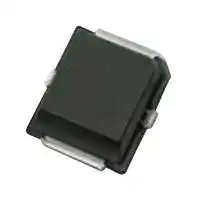
- Drain Source Voltage Vds:100V; Continuous Drain Current Id:-; Power Dissipation Pd:-; Operating Frequency Min:960MHz; Operating Frequency Max:1.4GHz; RF Transistor Case:PLD-1.5; No.
- MSL: MSL 3 - 168 hours
- SVHC: No SVHC (27-Jun-2024)
- No. of Pins: -
- Channel Type: N Channel
- Product Range: -
- Power Dissipation: -
- Transistor Mounting: Surface Mount
- Transistor Case Style: PLD-1.5
- Operating Frequency Max: 1.4GHz
- Operating Frequency Min: 960MHz
- Drain Source Voltage Vds: 100V
- Operating Temperature Max: 200°C
- Continuous Drain Current Id: -
| Delivery and price | |
|---|---|
| Units per pack | 100 |
| Price | 94.14 € |
| Current stock | 10+ |
| Lead time | 30 days |
**Freescale Semiconductor** Technical Data Document Number: MRF6V10010N Rev. 3, 7/2010 ## **RF Power Field Effect Transistor** ## N--Channel Enhancement--Mode Lateral MOSFET RF Power transistor designed for applications operating at frequencies between 960 and 1400 MHz, 1% to 20% duty cycle. This device is suitable for use in pulsed applications. - Typical Pulsed Performance: VDD = 50 Volts, IDQ = 10 mA, Pout = 10 Watts Peak (2 W Avg.), f = 1090 MHz, Pulse Width = 100 μsec, Duty Cycle = 20% Power Gain — 25 dB Drain Efficiency — 69% ## **Features** - Characterized with Series Equivalent Large--Signal Impedance Parameters ## **MRF6V10010NR4** **1090 MHz, 10 W, 50 V PULSED LATERAL N--CHANNEL RF POWER MOSFET** - Qualified Up to a Maximum of 50 VDD Operation - Integrated ESD Protection - Greater Negative Gate--Source Voltage Range for Improved Class C Operation - RoHS Compliant - In Tape and Reel. R4 Suffix = 100 Units per 12 mm, 7 inch Reel. **CASE 466--03, STYLE 1 PLD--1.5 PLASTIC** **Table 1. Maximum Ratings** |**Table 1. Maximum Ratings**|||| |---|---|---|---| |**Rating**|**Symbol**|**Value**|**Unit**| |Drain--Source Voltage|VDSS|--0.5, +100|Vdc| |Gate--Source Voltage|VGS|--6.0, +10|Vdc| |Storage Temperature Range|Tstg|-- 65 to +150|°C| |Case Operating Temperature|TC|150|°C| |Operating Junction Temperature|TJ|200|°C| |**Table 2. Thermal Characteristics**|||| |**Characteristic**|**Symbol**|**Value (1,2)**|**Unit**| |Thermal Resistance, Junction to Case|||| |Case Temperature 79°C, 10 W Pulsed, 100μsec Pulse Width, 20% Duty Cycle|ZθJC|1.6|°C/W| ## **Table 2. Thermal Characteristics** 1. MTTF calculator available at http://www.freescale.com/rf. Select Software & Tools/Development Tools/Calculators to access MTTF calculators by product. 2. Refer to AN1955, _Thermal Measurement Methodology of RF Power Amplifiers._ Go to http://www.freescale.com/rf. Select Documentation/Application Notes -- AN1955. © Freescale Semiconductor, Inc., 2008--2010. All rights reserved. **MRF6V10010NR4** RF Device Data Freescale Semiconductor 1 **Table 3. ESD Protection Characteristics** |**Table 3. ESD Protection Characteristics**|||||| |---|---|---|---|---|---| |**Test Methodology**||**Class**|||| |Human Body Model (per JESD22--A114)||1C (Minimum)|||| |Machine Model (per EIA/JESD22--A115)||A (Minimum)|||| |Charge Device Model (per JESD22--C101)||IV (Minimum)|||| |**Table 4. Moisture Sensitivity Level**|||||| |**Test Methodology**|**Rating**|**Package Peak Temperature**|||**Unit**| |Per JESD22--A113, IPC/JEDEC J--STD--020|3||260||°C| |**Table 5. Electrical Characteristics** (TA= 25°C unless otherwise noted)|||||| |**Characteristic**|**Symbol**|**Min**|**Typ**|**Max**|**Unit**| |**Off Characteristics**|||||| |Gate--Source Leakage Current<br>(VGS= 5 Vdc, VDS= 0 Vdc)|IGSS|—|—|10|μAdc| |Drain--Source Breakdown Voltage<br>(VGS= 0 Vdc, ID= 7 mA)|V(BR)DSS|100|—|—|Vdc| |Zero Gate Voltage Drain Leakage Current<br>(VDS= 50 Vdc, VGS= 0 Vdc)|IDSS|—|—|50|μAdc| |Zero Gate Voltage Drain Leakage Current<br>(VDS= 100 Vdc, VGS= 0 Vdc)|IDSS|—|—|2.5|mA| |**On Characteristics**|||||| |Gate Threshold Voltage<br>(VDS= 10 Vdc, ID= 36μAdc)|VGS(th)|1|1.7|2.5|Vdc| |Gate Quiescent Voltage<br>(VDD= 50 Vdc, ID= 10 mAdc, Measured in Functional Test)|VGS(Q)|1.7|2.4|3.2|Vdc| |Drain--Source On--Voltage<br>(VGS= 10 Vdc, ID= 70 mAdc)|VDS(on)|—|0.2|—|Vdc| |**Dynamic Characteristics**|||||| |Reverse Transfer Capacitance<br>(VDS= 50 Vdc±30 mV(rms)ac @ 1 MHz, VGS= 0 Vdc)|Crss|—|0.1|—|pF| |Output Capacitance<br>(VDS= 50 Vdc±30 mV(rms)ac @ 1 MHz, VGS= 0 Vdc)|Coss|—|3.38|—|pF| |Input Capacitance<br>(VDS= 50 Vdc, VGS= 0 Vdc±30 mV(rms)ac @ 1 MHz)|Ciss|—|9.55|—|pF| |**Functional Tests**(In Freescale Test Fixture, 50 ohm system) VDD= 50 Vdc, IDQ= 10 mA, Pout= 10 W Peak (2 W Avg.), f = 1090 MHz,<br>Pulsed, 100μsec Pulse Width, 20% Duty Cycle|||||| |Power Gain|Gps|23|25|28|dB| |Drain Efficiency|ηD|66|69|—|%| |Input Return Loss|IRL|_—_|--12|--8|dB| **MRF6V10010NR4** RF Device Data Freescale Semiconductor 2 **==> picture [492 x 235] intentionally omitted <==** **----- Start of picture text -----**<br> L1<br>VBIAS VSUPPLY<br>+<br>C9 C8 C7 C13<br>C2 C3 C12<br>R1<br>L2<br>RF<br>R2 C10 OUTPUT<br>Z8 Z9 Z10 Z11 Z12<br>RF<br>INPUT Z1 Z2 Z3 C5 Z4 C6 Z5 Z6 Z7 C14<br>C15 C11<br>C1<br>DUT<br>C16 C4<br>Z1 0.200″ x 0.080″ Microstrip Z8 0.367″ x 0.320″ Microstrip<br>Z2 0.696″ x 0.120″ Microstrip Z9 0.162″ x 0.320″ Microstrip<br>Z3 0.087″ x 0.320″ Microstrip Z10 0.757″ x 0.080″ Microstip<br>Z4 0.323″ x 0.320″ Microstrip Z11 0.763″ x 0.080″ Microstrip<br>Z5 0.320″ x 0.620″ x 0.185″ Taper Z12 0.290″ x 0.080″ Microstrip<br>Z6 0.135″ x 0.620″ Microstrip PCB Arlon CuClad 250GX--0300--55--22, 0.030″, εr = 2.55<br>Z7 0.714″ x 0.620″ Microstrip<br>**----- End of picture text -----**<br> **Figure 1. MR6V10010NR4 Test Circuit Schematic** **Table 6. MR6V10010NR4 Test Circuit Component Designations and Values** |**Part**|**Description**|**Part Number**|**Manufacturer**| |---|---|---|---| |C1, C9, C12|43 pF Chip Capacitors|ATC100B430JT500XT|ATC| |C2|10μF, 35 V Tantalum Capacitor|T491D106K035AT|Kemet| |C3, C8|2.2μF, 100 V Chip Capacitors|GQM1885C2A2R2CB01B|Murata| |C4, C6|7.5 pF Chip Capacitors|ATC100B7R5CT500XT|ATC| |C5, C16|3.0 pF Chip Capacitors|ATC100B3R0CT500XT|ATC| |C7|0.1μF Chip Capacitor|C1206C104K5RACTR|Kemet| |C10, C15|0.3 pF Chip Capacitors|ATC100B0R3BT500XT|ATC| |C11|5.6 pF Chip Capacitor|ATC100B5R6CT500XT|ATC| |C13|470μF, 63 V Chip Capacitor|477KXM063M|Illlinois Capacitor| |C14|47 pF Chip Capacitor|ATC100B470JT500XT|ATC| |L1|8 nH Inductor|A03TKLC|Coilcraft| |L2|5 nH Inductor|A02TKLC|Coilcraft| |R1|3300Ω, 1/4 W Chip Resistor|CRCW12063301FKEA|Vishay| |R2|10Ω, 1/4 W Chip Resistor|CRCW120610R0FKEA|Vishay| **MRF6V10010NR4** RF Device Data Freescale Semiconductor 3 **==> picture [402 x 242] intentionally omitted <==** **----- Start of picture text -----**<br> C7<br>L1 C3 C13<br>C2<br>C8<br>C12<br>R1<br>C9<br>R2<br>C16 C4 C15 L2 C14<br>C1<br>C5 C10<br>C6<br>C11<br>MRF6V10010N<br>Rev. 3<br>**----- End of picture text -----**<br> **Figure 2. MRF6V10010NR4 Test Circuit Component Layout** **MRF6V10010NR4** RF Device Data Freescale Semiconductor 4 ## **TYPICAL CHARACTERISTICS** **==> picture [235 x 175] intentionally omitted <==** **----- Start of picture text -----**<br> 100<br>Measured with ±30 mV(rms)ac @ 1 MHz<br>VGS = 0 Vdc<br>Ciss<br>10<br>Coss<br>1<br>Crss<br>0.1<br>0 10 20 30 40 50<br>VDS, DRAIN--SOURCE VOLTAGE (VOLTS)<br>C, CAPACITANCE (pF)<br>**----- End of picture text -----**<br> **Figure 3. Capacitance versus Drain--Source Voltage** **==> picture [235 x 175] intentionally omitted <==** **----- Start of picture text -----**<br> 10<br>TJ = 200°C<br>1 TJ = 175°C<br>TJ = 150°C<br>TC = 25°C<br>0.1<br>1 10 100<br>VDS, DRAIN--SOURCE VOLTAGE (VOLTS)<br>, DRAIN CURRENT (AMPS)<br>ID<br>**----- End of picture text -----**<br> **Figure 4. DC Safe Operating Area** **==> picture [255 x 416] intentionally omitted <==** **----- Start of picture text -----**<br> 27 75<br>Gps<br>26 70<br>25 65<br>ηD<br>24 60<br>23 55<br>VDD = 50 Vdc, IDQ = 10 mA, f = 1090 MHz<br>Pulse Width = 100 μsec, Duty Cycle = 20%<br>22 50<br>5 6 7 8 9 10 11 12<br>Pout, OUTPUT POWER (WATTS) PULSED<br>Figure 5. Pulsed Power Gain and Drain Efficiency<br>versus Output Power<br>27<br>25<br>23<br>50 V<br>45 V<br>21<br>40 V<br>35 V<br>19 IDQ = 10 mA, f = 1090 MHz<br>VDD = 30 V Pulse Width = 100 μsec<br>Duty Cycle = 20%<br>17<br>0 2 4 6 8 10 12<br>Pout, OUTPUT POWER (WATTS) PULSED<br>Figure 7. Pulsed Power Gain versus<br>Output Power<br>, POWER GAIN (dB)<br>ps DRAIN EFFICIENCY (%)<br>G D,<br>η<br>, POWER GAIN (dB)<br>ps<br>G<br>**----- End of picture text -----**<br> **==> picture [236 x 391] intentionally omitted <==** **----- Start of picture text -----**<br> 45<br>P3dB = 40.66 dBm (11.65 W) Ideal<br>P1dB = 40.18 dBm<br>(10.42 W)<br>Actual<br>40<br>VDD = 50 Vdc, IDQ = 10 mA, f = 1090 MHz<br>Pulse Width = 100 μsec, Duty Cycle = 20%<br>35<br>12 13 14 15 16 17 18 19<br>Pin, INPUT POWER (dBm) PULSED<br>Figure 6. Pulsed Output Power versus<br>Input Power<br>14<br>TC = --30 _ C<br>12<br>85 _ C<br>10<br>25 _ C<br>8<br>6<br>VDD = 50 Vdc<br>4 IDQ = 10 mA<br>f = 1090 MHz<br>2 Pulse Width = 100 μsec<br>Duty Cycle = 20%<br>0<br>0 0.01 0.02 0.03 0.04 0.05 0.06 0.07<br>Pin, INPUT POWER (WATTS) PULSED<br>, OUTPUT POWER (dBm) PULSED<br>out<br>P<br>, OUTPUT POWER (WATTS) PULSED<br>out<br>P<br>**----- End of picture text -----**<br> **Figure 8. Pulsed Output Power versus Input Power** **MRF6V10010NR4** RF Device Data Freescale Semiconductor 5 ## **TYPICAL CHARACTERISTICS** **==> picture [258 x 459] intentionally omitted <==** **----- Start of picture text -----**<br> 29 80<br>ηD<br>28 70<br>27 60<br>TC = --30 _ C<br>26 25 _ C 50<br>25 40<br>85 _ C<br>Gps<br>24 30<br>23 VDD = 50 Vdc, IDQ = 10 mA, f = 1090 MHz 20<br>Pulse Width = 100 μsec, Duty Cycle = 20%<br>22 10<br>0 2 4 6 8 10 12 14<br>Pout, OUTPUT POWER (WATTS) PULSED<br>Figure 9. Pulsed Power Gain and Drain Efficiency<br>versus Output Power<br>10 [9]<br>10 [8]<br>10 [7]<br>10 [6]<br>10 [5]<br>90 110 130 150 170 190 210 230 250<br>TJ, JUNCTION TEMPERATURE (°C)<br>This above graph displays calculated MTTF in hours when the device<br>is operated at VDD = 50 Vdc, Pout = 10 W Peak, Pulse Width = 100 μsec,<br>Duty Cycle = 20%, and ηD = 69%.<br>MTTF calculator available at http://www.freescale.com/rf. Select<br>Software & Tools/Development Tools/Calculators to access MTTF<br>calculators by product.<br>, POWER GAIN (dB)<br>ps DRAIN EFFICIENCY (%)<br>G D,<br>η<br>MTTF (HOURS)<br>**----- End of picture text -----**<br> **Figure 10. MTTF versus Junction Temperature** **MRF6V10010NR4** RF Device Data Freescale Semiconductor 6 **==> picture [376 x 187] intentionally omitted <==** **----- Start of picture text -----**<br> A<br>Zo = 50 Ω<br>Score dT :<br>oP ATL LESS<br>o% hyFEE «3 Vi89 oseeeetestewSASK Zload SETSs oe[~<br>PLP /% KPSEX> SoO eT Saaraas<br>ORSERE ELSSP f = 1090 MHz AE LLTy<br>yalf LPRbpREESE EEREDRED OD OnOchoa CCEACCCOoa<br>VIER ES EL HH<br>sis/Sh PL) Z ° source LEISCEERI ODESRIL KK KO OOK IA<br>ST f [7 LEER RE LCR ROSSI SATE<br>Tob bel be PIRIIL L RO ROOLOSK HI GEL<br>/8f B3 o, LET LEE LK KK RERK SSSSEKEL<br>Lis Strb f = 1090 MHz L RREROLOKOLED<br>| Bis PE EE TAL IIRL KK SS SSO<br>& schseseteetees pL EE OK LL REE BORS<br>FL SHER CEE AT LAOASG >, LALOR ‘oS<br>**----- End of picture text -----**<br> VDD = 50 Vdc, IDQ = 10 mA, Pout = 10 W Peak **==> picture [190 x 187] intentionally omitted <==** **----- Start of picture text -----**<br> f Zsource Zload<br>MHz Ω Ω<br>1090 1.15 + j8.96 13.47 + j34.32<br>Zsource = Test circuit impedance as measured from<br>gate to ground.<br>Zload = Test circuit impedance as measured<br>from drain to ground.<br>Input Device Output<br>Matching Under Matching<br>Network Test Network<br>Zsource Zload<br>**----- End of picture text -----**<br> **Figure 11. Series Equivalent Source and Load Impedance** **MRF6V10010NR4** RF Device Data Freescale Semiconductor 7 ## **PACKAGE DIMENSIONS** **==> picture [473 x 362] intentionally omitted <==** **----- Start of picture text -----**<br> 0.146<br>A<br>3.71<br>F<br>0.095<br>2.41<br>3 0.115<br>2.92<br>B D 1 2 R L 0.115<br>2.92<br>0.020<br>0.51<br>4<br>N 0.35 (0.89) X 45 _ 5 _ inches<br>K 10 _ DRAFT mm<br>SOLDER FOOTPRINT<br>Q<br>U P INCHES MILLIMETERS<br>ZONE V H4 C Y Y E DIMAB 0.2550.225 MIN 0.2650.235 MAX MIN 6.485.72 MAX 6.735.97<br>C 0.065 0.072 1.65 1.83<br>D 0.130 0.150 3.30 3.81<br>NOTES:<br>E 0.021 0.026 0.53 0.66<br>1. INTERPRET DIMENSIONS AND TOLERANCES<br>ZONE W PER ASME Y14.5M, 1984. F 0.026 0.044 0.66 1.12<br>1 2 2. CONTROLLING DIMENSION: INCH G 0.050 0.070 1.27 1.78<br>3. RESIN BLEED/FLASH ALLOWABLE IN ZONE V, W, H 0.045 0.063 1.14 1.60<br>AND X. J 0.160 0.180 4.06 4.57<br>K 0.273 0.285 6.93 7.24<br>STYLE 1: L 0.245 0.255 6.22 6.48<br>PIN 1. DRAIN N 0.230 0.240 5.84 6.10<br>3 2. GATE P 0.000 0.008 0.00 0.20<br>S 3.4. SOURCESOURCE Q 0.055 0.063 1.40 1.60<br>G ZONE X R 0.200 0.210 5.08 5.33<br>S 0.006 0.012 0.15 0.31<br>U 0.006 0.012 0.15 0.31<br>VIEW Y--Y CASE 466--03 ZONE V 0.000 0.021 0.00 0.53<br>ISSUE D ZONE WZONE X 0.0000.000 0.0100.010 0.000.00 0.250.25<br>PLD--1.5<br>PLASTIC<br>**----- End of picture text -----**<br> **MRF6V10010NR4** RF Device Data Freescale Semiconductor 8 ## **PRODUCT DOCUMENTATION AND SOFTWARE** Refer to the following documents to aid your design process. ## **Application Notes** - AN1955: Thermal Measurement Methodology of RF Power Amplifiers ## **Engineering Bulletins** - EB212: Using Data Sheet Impedances for RF LDMOS Devices ## **Software** - Electromigration MTTF Calculator For Software, do a Part Number search at http://www.freescale.com, and select the “Part Number” link. Go to the Software & Tools tab on the part’s Product Summary page to download the respective tool. ## **REVISION HISTORY** The following table summarizes revisions to this document. |**Revision**|**Date**|**Description**| |---|---|---| |0|June 2008|•<br>Initial Release of Data Sheet| |1|Feb. 2009|•<br>Corrected Zsource, “2.57 -- j7.33” to “1.15 + j8.96” and Zload, “14.10 -- j34.77” to “13.47 + j34.32” in Fig. 11,<br>Series Equivalent Source and Load Impedance data table and replotted data, p. 7| |2|June 2009|•<br>Modified data sheet to reflect MSL rating change from 1 to 3 as a result of the standardization of packing<br>process as described in Product and Process Change Notification number, PCN13516, p. 2<br>•<br>Added Electromigration MTTF Calculator availability to Product Documentation, Tools and Software, p. 9| |3|July 2010|•<br>Reporting of pulsed thermal data now shown using the ZθJCsymbol, Table 2, Thermal Characteristics, p. 1<br>•<br>Corrected errors made in the translation of the printed circuit board to the schematic, Fig. 1, Test Circuit<br>Schematic and Z list, p. 3| **MRF6V10010NR4** RF Device Data Freescale Semiconductor 9 **==> picture [505 x 59] intentionally omitted <==** ## _**How to Reach Us:**_ **Home Page:** www.freescale.com ## **Web Support:** http://www.freescale.com/support **USA/Europe or Locations Not Listed:** Freescale Semiconductor, Inc. Technical Information Center, EL516 2100 East Elliot Road Tempe, Arizona 85284 1--800--521--6274 or +1--480--768--2130 www.freescale.com/support ## **Europe, Middle East, and Africa:** Freescale Halbleiter Deutschland GmbH Technical Information Center Schatzbogen 7 81829 Muenchen, Germany +44 1296 380 456 (English) +46 8 52200080 (English) +49 89 92103 559 (German) +33 1 69 35 48 48 (French) www.freescale.com/support ## **Japan:** Freescale Semiconductor Japan Ltd. Headquarters ARCO Tower 15F 1--8--1, Shimo--Meguro, Meguro--ku, Tokyo 153--0064 Japan 0120 191014 or +81 3 5437 9125 support.japan@freescale.com **Asia/Pacific:** Freescale Semiconductor China Ltd. Exchange Building 23F No. 118 Jianguo Road Chaoyang District Beijing 100022 China +86 10 5879 8000 support.asia@freescale.com ## _**For Literature Requests Only:**_ Freescale Semiconductor Literature Distribution Center 1--800--441--2447 or +1--303--675--2140 Fax: +1--303--675--2150 LDCForFreescaleSemiconductor@hibbertgroup.com Information in this document is provided solely to enable system and software implementers to use Freescale Semiconductor products. There are no express or implied copyright licenses granted hereunder to design or fabricate any integrated circuits or integrated circuits based on the information in this document. Freescale Semiconductor reserves the right to make changes without further notice to any products herein. Freescale Semiconductor makes no warranty, representation or guarantee regarding the suitability of its products for any particular purpose, nor does Freescale Semiconductor assume any liability arising out of the application or use of any product or circuit, and specifically disclaims any and all liability, including without limitation consequential or incidental damages. “Typical” parameters that may be provided in Freescale Semiconductor data sheets and/or specifications can and do vary in different applications and actual performance may vary over time. All operating parameters, including “Typicals”, must be validated for each customer application by customer’s technical experts. Freescale Semiconductor does not convey any license under its patent rights nor the rights of others. Freescale Semiconductor products are not designed, intended, or authorized for use as components in systems intended for surgical implant into the body, or other applications intended to support or sustain life, or for any other application in which the failure of the Freescale Semiconductor product could create a situation where personal injury or death may occur. Should Buyer purchase or use Freescale Semiconductor products for any such unintended or unauthorized application, Buyer shall indemnify and hold Freescale Semiconductor and its officers, employees, subsidiaries, affiliates, and distributors harmless against all claims, costs, damages, and expenses, and reasonable attorney fees arising out of, directly or indirectly, any claim of personal injury or death associated with such unintended or unauthorized use, even if such claim alleges that Freescale Semiconductor was negligent regarding the design or manufacture of the part. Freescale t and the Freescale logo are trademarks of Freescale Semiconductor, Inc. All other product or service names are the property of their respective owners. © Freescale Semiconductor, Inc. 2008--2010. All rights reserved. ## **MRF6V10010NR4** **==> picture [96 x 32] intentionally omitted <==** RF Device Data Freescale Semiconductor Document Number: MRF6V10010N 10Rev. 3, 7/2010
Updated at April 10, 2026
NXP Semiconductors is a global leader in secure connectivity solutions, driving innovation across the automotive, industrial, IoT, mobile, and communications infrastructure markets. By developing advanced, purpose-built technologies, NXP enables devices to sense, think, connect, and act intelligently, delivering rigorously tested components that make the connected world safer and more efficient. Within the semiconductor space, NXP is highly regarded for its extensive range of high-performance integrated circuits and discrete devices. The brand's portfolio excels in drivers and interfaces, featuring a comprehensive selection of I/O expanders designed to streamline complex system architectures. For demanding high-frequency and wireless applications, NXP provides industry-leading RF FETs and RF/PIN diodes engineered to deliver exceptional signal integrity, efficiency, and reliability. The NXP product lineup further extends to essential discrete components, including versatile bipolar transistors, JFETs, and small signal diodes optimized for precision switching and amplification. Additionally, the portfolio supports advanced automation and smart applications with precision IC sensors, such as MEMS accelerometers, alongside specialized power management solutions like AC/DC LED driver ICs and single MOSFETs for cutting-edge electronics design.
About Novapart
Novapart is a B2B electronic component broker specialising in stock shortages and cost reduction. We source hard-to-find parts and identify compliant alternatives across a catalogue of 410,000+ components from 500+ manufacturers.
Learn more →Stock Shortage Specialist
When a component is unavailable, discontinued or has an unacceptable lead time, we tap into our network of vetted European and Asian distributors to source what you need — without compromising on quality or traceability.
Request a quote →Compliant Alternatives
We identify pin-to-pin, electrically equivalent substitutes that meet the same certifications (RoHS, AEC-Q100, REACH) as your original specification — validated against datasheets, not just part numbers. Often at a lower cost.
BOM Analysis service →