
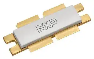


MRF1K50HR5
RF FET Transistor, 135 VDC, 1.667 kW, 1.8 MHz, 500 MHz, NI-1230
- Manufacturer: NXP
- Product type: RF FETs
- Drain Source Voltage Vds:135VDC; Continuous Drain Current Id:-; Power Dissipation Pd:1.667kW; Operating Frequency Min:1.8MHz; Operating Frequency Max:500MHz; RF Transistor Case:NI-1230; N
- MSL: -
- SVHC: No SVHC (27-Jun-2024)
- No. of Pins: 4Pins
- Channel Type: N Channel
- Product Range: -
- Power Dissipation: 1.667kW
- Transistor Mounting: Flange
- Transistor Case Style: NI-1230
- Operating Frequency Max: 500MHz
- Operating Frequency Min: 1.8MHz
- Drain Source Voltage Vds: 135VDC
- Operating Temperature Max: 225°C
- Continuous Drain Current Id: -
| Delivery and price | |
|---|---|
| Units per pack | 5 |
| Price | 287.36 € |
| Current stock | 25+ |
| Lead time | 30 days |
NXP Semiconductors Technical Data Document Number: MRF1K50H Rev. 1.1, 03/2017 ## RF Power LDMOS Transistor High Ruggedness N--Channel Enhancement--Mode Lateral MOSFET This high ruggedness device is designed for use in high VSWR industrial, scientific and medical applications, as well as radio and VHF TV broadcast, sub--GHz aerospace and mobile radio applications. Its unmatched input and output design allows for wide frequency range use from 1.8 to 500 MHz. Typical Performance: VDD = 50 Vdc MRF1K50H 1.8–500 MHz, 1500 W CW, 50 V WIDEBAND RF POWER LDMOS TRANSISTOR ~~ee~~ Frequency Pout Gps **η** D (MHz) Signal Type (W) (dB) (%) 27 CW 1550 CW 25.9 78.3 81.36[(1)] CW 1400 CW 23.0 75.0 87.5–108[(2,3)] CW 1475 CW 23.3 83.4 230[(4)] Pulse 1500 Peak 23.7 74.0 (100 µsec, 20% Duty Cycle) NI--1230H--4S Load Mismatch/Ruggedness Frequency Pin Test ~~SSS SSS | Fe~~ (MHz) Signal Type VSWR (W) Voltage Result 230[(4)] Pulse > 65:1 at all 13 Peak 50 No Device Gate A 3 1 Drain A (100 µsec, 20% Phase Angles (3 dB Degradation Duty Cycle) Overdrive) 1. Data from 81.36 MHz narrowband reference circuit (page 11). 2. Data from 87.5–108 MHz broadband reference circuit (page 5). Gate B 4 2 Drain B 3. The values shown are the center band performance numbers across the indicated frequency range. 4. Data from 230 MHz narrowband production test fixture (page 16). (Top View) Features • High drain--source avalanche energy absorption capability Note: The backside of the package is the source terminal for the transistor. • Unmatched input and output allowing wide frequency range utilization • Figure 1. Pin Connections Device can be used single--ended or in a push--pull configuration ~~lca~~ • Characterized from 30 to 50 V for ease of use • Suitable for linear application - Integrated ESD protection with greater negative gate--source voltage range for improved Class C operation - Recommended driver: MRFE6VS25N (25 W) - Lower thermal resistance part available: MRF1K50N - Included in NXP product longevity program with assured supply for a minimum of 15 years after launch ## Typical Applications - Industrial, scientific, medical (ISM) - Laser generation - Plasma etching - Particle accelerators - MRI and other medical applications - Industrial heating, welding and drying systems - Broadcast - Radio broadcast - VHF TV broadcast - Aerospace – VHF omnidirectional range (VOR) - – HF and VHF communications – Weather radar - • Mobile radio – VHF and UHF base stations 2016–2017 NXP B.V. MRF1K50H RF Device Data ~~NP~~ NXP Semiconductors MRF1K50H 1 Table 1. Maximum Ratings |Table 1. Maximum Ratings|||| |---|---|---|---| |Rating|Symbol|Value|Unit| |Drain--Source Voltage|VDSS|–0.5, +135|Vdc| |Gate--Source Voltage|VGS|–6.0, +10|Vdc| |Operating Voltage|VDD|50|Vdc| |Storage Temperature Range|Tstg|–65 to +150|°C| |Case Operating Temperature Range|TC|–40 to +150|°C| |Operating Junction Temperature Range (1,2)|TJ|–40 to +225|°C| |Total Device Dissipation @ TC= 25°C<br>Derate above 25°C|PD|1667<br>8.33|W<br>W/°C| |Table 2. Thermal Characteristics|||| |Characteristic|Symbol|Value (2,3)|Unit| |Thermal Resistance, Junction to Case<br>CW: Case Temperature 78°C, 1500 W CW, 50 Vdc, IDQ(A+B)= 200 mA, 88 MHz|RθJC|0.10|°C/W| |Thermal Impedance, Junction to Case<br>Pulse: Case Temperature 73°C, 1500 W Peak, 100µsec Pulse Width, 20% Duty Cycle,<br>IDQ(A+B)= 100 mA, 230 MHz|ZθJC|0.028|°C/W| ## Table 3. ESD Protection Characteristics |Table 3. ESD Protection Characteristics|Table 3. ESD Protection Characteristics||||| |---|---|---|---|---|---| |Test Methodology|||Class||| |Human Body Model (per JESD22--A114)|||2, passes 2500 V||| |Machine Model (per EIA/JESD22--A115)|||B, passes 250 V||| |Charge Device Model (per JESD22--C101)|||IV, passes 2000 V||| |Table 4. Electrical Characteristics (TA= 25°C unless otherwise noted)|||||| |Characteristic|Symbol|Min|Typ|Max|Unit| |Off Characteristics (4)|||||| |Gate--Source Leakage Current<br>(VGS= 5 Vdc, VDS= 0 Vdc)|IGSS|—|—|1|µAdc| |Drain--Source Breakdown Voltage<br>(VGS= 0 Vdc, ID= 30µAdc)|V(BR)DSS|135|—|—|Vdc| |Zero Gate Voltage Drain Leakage Current<br>(VDS= 50 Vdc, VGS= 0 Vdc)|IDSS|—|—|10|µAdc| |Zero Gate Voltage Drain Leakage Current<br>(VDS= 100 Vdc, VGS= 0 Vdc)|IDSS|—|—|20|µAdc| |On Characteristics|||||| |Gate Threshold Voltage (4)<br>(VDS= 10 Vdc, ID= 2130µAdc)|VGS(th)|1.7|2.2|2.7|Vdc| |Gate Quiescent Voltage<br>(VDD= 50 Vdc, ID(A+B)= 100 mAdc, Measured in Functional Test)|VGS(Q)|1.9|2.4|2.9|Vdc| |Drain--Source On--Voltage (4)<br>(VGS= 10 Vdc, ID= 2.4 Adc)|VDS(on)|—|0.15|—|Vdc| |Forward Transconductance (4)<br>(VDS= 10 Vdc, ID= 36 Adc)|gfs|—|33.5|—|S| 1. Continuous use at maximum temperature will affect MTTF. 2. MTTF calculator available at http://www.nxp.com/RF/calculators. 3. Refer to AN1955, Thermal Measurement Methodology of RF Power Amplifiers. Go to http://www.nxp.com/RF and search for AN1955. 4. Each side of device measured separately. (continued) MRF1K50H RF Device Data NXP Semiconductors 2 Table 4. Electrical Characteristics (TA = 25°C unless otherwise noted) (continued) |Characteristic|Symbol|Min|Typ|Max|Unit| |---|---|---|---|---|---| |Dynamic Characteristics (1)|||||| |Reverse Transfer Capacitance<br>(VDS= 50 Vdc±30 mV(rms)ac @ 1 MHz, VGS= 0 Vdc)|Crss|—|3.48|—|pF| |Output Capacitance<br>(VDS= 50 Vdc±30 mV(rms)ac @ 1 MHz, VGS= 0 Vdc)|Coss|—|205|—|pF| |Input Capacitance<br>(VDS= 50 Vdc, VGS= 0 Vdc±30 mV(rms)ac @ 1 MHz)|Ciss|—|664|—|pF| |Functional Tests(In NXP Production Test Fixture, 50 ohm system) VDD= 50 Vdc, IDQ(A+B)= 100 mA, Pout= 1500 W Peak (300 W Avg.),<br>f = 230 MHz, 100µsec Pulse Width, 20% Duty Cycle|||||| |Power Gain|Gps|22.5|23.7|25.5|dB| |Drain Efficiency|ηD|70.0|74.0|—|%| |Input Return Loss|IRL|—|–18.3|–9|dB| Table 5. Load Mismatch/Ruggedness (In NXP Production Test Fixture, 50 ohm system) IDQ(A+B) = 100 mA |Frequency<br>(MHz)|Signal Type|Signal Type|VSWR|Pin<br>(W)|Test Voltage, VDD|Test Voltage, VDD|Result| |---|---|---|---|---|---|---|---| |230|Pulse<br>(100µsec, 20% Duty Cycle)||> 65:1 at all<br>Phase Angles|13 Peak<br>(3 dB Overdrive)|50||No Device Degradation| |Table 6. Ordering Information|||||||| |Device|||Tape and Reel Information||||Package| |MRF1K50HR5||R5 Suffix =|50 Units, 56 mm Tape Width, 13--inch Reel|||NI--1230H--4S|| 1. Each side of device measured separately. MRF1K50H RF Device Data NXP Semiconductors 3 ## TYPICAL CHARACTERISTICS **==> picture [242 x 471] intentionally omitted <==** **----- Start of picture text -----**<br> 10000<br>Measured with ±30 mV(rms)ac @ 1 MHz<br>V GS = 0 Vdc<br>1000 Ciss<br>Coss<br>100<br>C rss<br>10<br>1<br>0 10 20 30 40 50<br>VDS, DRAIN--SOURCE VOLTAGE (VOLTS)<br>Note: Each side of device measured separately.<br>Figure 2. Capacitance versus Drain--Source Voltage<br>0.11<br>0.09<br>D = 0.7<br>0.07<br>D = 0.5<br>0.05<br>PD t 1<br>D = 0.3<br>0.03 t 2<br>D = Duty Factor = t1/t2<br>0.01 D = 0.1 t t1 2 = Pulse Width = Pulse Period<br>TJ = PD * ZJC + TC<br>0<br>0.00001 0.0001 0.001 0.01 0.1 1 10<br>RECTANGULAR PULSE WIDTH (S)<br>C, CAPACITANCE (pF)<br>C/W)<br>°<br>, THERMAL IMPEDANCE (<br>JC<br>Z<br>**----- End of picture text -----**<br> Figure 2. Capacitance versus Drain--Source Voltage Figure 4. Maximum Transient Thermal Impedance **==> picture [240 x 254] intentionally omitted <==** **----- Start of picture text -----**<br> 1.08<br>500 mA<br>IDQ(A+B) = 100 mA VDD = 50 Vdc<br>1.06<br>1.04<br>1500 mA<br>1.02<br>2000 mA<br>1<br>0.98<br>0.96<br>0.94<br>0.92<br>–50 –25 0 25 50 75 100<br>TC, CASE TEMPERATURE (°C)<br>IDQ (mA) Slope (mV/ ° C)<br>100 –2.87<br>500 –2.56<br>1500 –2.29<br>2000 –2.11<br>GS(Q)<br>NORMALIZED V<br>**----- End of picture text -----**<br> Figure 3. Normalized VGS versus Quiescent Current and Case Temperature **==> picture [239 x 212] intentionally omitted <==** **----- Start of picture text -----**<br> 10 [8]<br>V DD = 50 Vdc<br>10 [7] ID = 36.0 Amps<br>10 [6]<br>10 [5]<br>10 [4]<br>10 [3]<br>90 110 130 150 170 190 210 230 250<br>TJ, JUNCTION TEMPERATURE (°C)<br>Note: MTTF value represents the total cumulative operating time<br>under indicated test conditions.<br>MTTF calculator available at http:/www.nxp.com/RF/calculators.<br>MTTF (HOURS)<br>**----- End of picture text -----**<br> Figure 5. MTTF versus Junction Temperature — CW MRF1K50H RF Device Data NXP Semiconductors 4 ## 87.5–108 MHz BROADBAND REFERENCE CIRCUIT Table 7. 87.5–108 MHz Broadband Performance (In NXP Reference Circuit, 50 ohm system) VDD = 50 Vdc, IDQ(A+B) = 200 mA, Pin = 7 W, CW |VDD= 50 Vdc, IDQ(A+B)= 200|mA, Pin= 7 W, CW||| |---|---|---|---| |Frequency<br>(MHz)|Gps<br>(dB)|**η**D<br>(%)|Pout<br>(W)| |87.5|22.8|81.8|1325| |98|23.3|83.4|1475| |108|23.0|81.2|1410| MRF1K50H RF Device Data NXP Semiconductors 5 ## 87.5–108 MHz BROADBAND REFERENCE CIRCUIT — 2.88 **″ ×** 5.12 **″** (73 mm **×** 130 mm) **==> picture [371 x 336] intentionally omitted <==** **----- Start of picture text -----**<br> C6 C7 C25 C22 C26 C21 C27 L4<br>C28<br>C5<br>L1 R2 C20<br>C19<br>C4<br>C18<br>R1 C11 C17<br>C3 Q1 C16<br>C12 C24<br>C1<br>C2* L3 C23*<br>L2 C15*<br>R3<br>C8 C13 [C14*]<br>C9 C10 MRF1K50H<br>Rev. 0 D62499<br>*C2, C14, C15 and C23 are mounted vertically.<br>Note: Q1 leads are soldered to the PCB with L3 soldered directly on top of the drain leads.<br>0.26<br>(6.5)<br>0.63<br>(16.0)<br>0.26<br>(6.6)<br>Inches<br>L3 total wire length = 2.04″ (52 mm) (mm)<br>**----- End of picture text -----**<br> Figure 6. MRF1K50H 87.5–108 MHz Broadband Reference Circuit Component Layout Figure 7. MRF1K50H 87.5–108 MHz Broadband Reference Circuit Component Layout — Bottom MRF1K50H RF Device Data NXP Semiconductors 6 ## 87.5–108 MHz BROADBAND REFERENCE CIRCUIT Table 8. MRF1K50H Broadband Reference Circuit Component Designations and Values — 87.5–108 MHz |Part|Description|Part Number|Manufacturer| |---|---|---|---| |C1, C3, C6, C9, C18, C19,<br>C20, C21, C22|1000 pF Chip Capacitors|ATC100B102JT50XT|ATC| |C2|33 pF Chip Capacitor|ATC100B330JT500XT|ATC| |C4, C5, C8|10,000 pF Chip Capacitors|ATC200B103KT50XT|ATC| |C7, C10, C15, C16, C17, C23|470 pF Chip Capacitors|ATC100B471JT200XT|ATC| |C11|91 pF 300 V Mica Capacitor|MIN02-002EC910J-F|CDE| |C12|56 pF 300 V Mica Capacitor|MIN02-002DC560J-F|CDE| |C13|2.2 pF Chip Capacitor|ATC100B2R2JT500XT|ATC| |C14, C24|12 pF Chip Capacitors|ATC100B120GT500XT|ATC| |C25, C26, C27|220µF, 63 V Electrolytic Capacitors|EEV-FK2A221M|Panasonic| |C28|22µF, 35 V Electrolytic Capacitor|UUD1V220MCL1GS|Nichicon| |L1, L2|17.5 nH Inductors, 6 Turns|B06TJLC|Coilcraft| |L3|1.5 mm Non--Tarnish Silver Plated Copper Wire|SP1500NT-001|Scientific Wire Company| |L4|22 nH Inductor|1212VS-22NMEB|Coilcraft| |Q1|RF Power LDMOS Transistor|MRF1K50H|NXP| |R1|10Ω, 1/4 W Chip Resistor|CRCW120610R0JNEA|Vishay| |R2, R3|33Ω, 2 W Chip Resistors|1-2176070-3|TE Connectivity| |PCB|Arlon TC350 0.030″,εr= 3.5|D62499|MTL| Note: Refer to MRF1K50H’s printed circuit boards and schematics to download the 87.5–108 MHz heatsink drawing. MRF1K50H RF Device Data NXP Semiconductors 7 ## TYPICAL CHARACTERISTICS — 87.5–108 MHz BROADBAND REFERENCE CIRCUIT **==> picture [282 x 175] intentionally omitted <==** **----- Start of picture text -----**<br> 27 85<br>26 83<br>ηD<br>25 81<br>24 79<br>23 77<br>Gps<br>22 1600<br>21 1500<br>Pout<br>20 1400<br>19 1300<br>VDD = 50 Vdc, Pin = 7 W, lDQ(A+B) = 200 mA<br>18 1200<br>87 89 91 93 95 97 99 101 103 105 107 109<br>f, FREQUENCY (MHz)<br>, DRAIN<br>D<br>η<br>EFFICIENCY (%)<br>, POWER GAIN (dB)<br>ps<br>G<br>, OUTPUT<br>out<br>P<br>POWER (WATTS)<br>**----- End of picture text -----**<br> Figure 8. Power Gain, Drain Efficiency and CW Output Power versus Frequency at a Constant Input Power **==> picture [288 x 388] intentionally omitted <==** **----- Start of picture text -----**<br> 1600<br>1400<br>87.5 MHz<br>1200<br>1000 98 MHz<br>800<br>108 MHz<br>600<br>400<br>200 V DD = 50 Vdc, I DQ(A+B) = 200 mA<br>0<br>0 1 2 3 4 5 6 7 8 9<br>Pin, INPUT POWER (WATTS)<br>Figure 9. CW Output Power versus Input Power and Frequency<br>30 100<br>f = 87.5 MHz<br>29 80<br>ηD 98 MHz<br>28 108 MHz 60<br>27 87.5 MHz 40<br>26 20<br>98 MHz<br>108 MHz<br>25 1600<br>24 87.5 MHz 1200<br>23 800<br>Pout 98 MHz Gps<br>22 400<br>108 MHz VDD = 50 Vdc, lDQ(A+B) = 200 mA<br>21 0<br>0 1 2 3 4 5 6 7 8 9<br>Pin, INPUT POWER (WATTS)<br>, OUTPUT POWER (WATTS) PEAK<br>out<br>P<br>, DRAIN<br>D<br>η<br>EFFICIENCY (%)<br>, POWER GAIN (dB)<br>ps<br>G<br>, OUTPUT<br>out<br>P<br>POWER (WATTS)<br>**----- End of picture text -----**<br> Figure 9. CW Output Power versus Input Power and Frequency Figure 10. Power Gain, Drain Efficiency and CW Output Power versus Input Power and Frequency MRF1K50H RF Device Data NXP Semiconductors 8 ## 87.5–108 MHz BROADBAND REFERENCE CIRCUIT **==> picture [399 x 434] intentionally omitted <==** **----- Start of picture text -----**<br> BLALfc k>bXKEESON OOSSSX OeCYTSe HAST Zo = 10 Ω a eeaeey,S i»<%<br>LBKS KLRRREOEOXDRRL Zsource SSOCSO [SE] AEE [S] L [S] ETH PpLAQSiS<br>lahys RELLY CxS} chee ALS<br>ROE f = 108 MHz RL f = 87.5 MHz CX X SI hy S,<br> PLIEFel PR R SELEDEPRy ne PROSIIPO EEE T TAE<br>f = 108 MHz<br>f = 87.5 MHz<br>a eae PADI PASO 2 OK PH<br>EE area pease ace Zload re LTALH POL LOREIL DRL KROL [ROSE] eoceteennet<br> PESEEREREE PE ATT TE RSE<br>Beeasfefssiiii7issi: 2 eeenaneenerse si owes ee eee eee,SPREE<br>Hereeeerteey EPHPy ed fy<br>erererrrepte = EHEEEEE CCE<br>eece Bestneetennc. 4<br>f Zsource Zload<br>MHz Ω Ω<br>87.5 4.07 + j5.13 3.92 + j2.89<br>98 3.93 + j4.84 3.39 + j2.35<br>108 3.50 + j4.72 2.83 + j2.56<br>Zsource = Test circuit impedance as measured from<br>gate to gate, balanced configuration.<br>Zload = Test circuit impedance as measured<br>from drain to drain, balanced configuration.<br>Input Device Output<br>Matching + Under -- Matching<br>Network Test Network<br>50 Ω 50 Ω<br>-- +<br>Zsource Zload<br>**----- End of picture text -----**<br> Figure 11. Broadband Series Equivalent Source and Load Impedance — 87.5–108 MHz MRF1K50H RF Device Data NXP Semiconductors 9 ## HARMONIC MEASUREMENTS — 87.5–108 MHz BROADBAND REFERENCE CIRCUIT **==> picture [417 x 223] intentionally omitted <==** **----- Start of picture text -----**<br> F1 87.5 MHz<br>Fundamental (F1)<br>H2 175 MHz –30 dB<br>ee | | | H3 262.5 MHz –28 dB<br>H2 H3 H4<br>H4 350 MHz –46 dB<br>(175 MHz) (262.5 MHz) (350 MHz)<br>faaaeet ee<br>–30 dB –28 dB –46 dB<br>H3<br>Pet Tt | y t le | EL _} +<br>PLT EA H2 E<br>H4<br>PL | TAL Eh EEE L<br>ve | RPK URN | PTY WO<br>pj f | | ft} py<br>Center: 228.5 MHz 35 MHz Span: 350 MHz<br>**----- End of picture text -----**<br> Figure 12. 87.5 MHz Harmonics @ 1200 W CW MRF1K50H RF Device Data NXP Semiconductors 10 ## 81.36 MHz NARROWBAND REFERENCE CIRCUIT Table 9. 81.36 MHz Narrowband Performance (In NXP Reference Circuit, 50 ohm system) VDD = 50 Vdc, IDQ(A+B) = 150 mA, Pin = 3 W, CW |VDD= 50 Vdc, IDQ(A+B)= 150|mA, Pin= 3 W, CW||| |---|---|---|---| |Frequency<br>(MHz)|Gps<br>(dB)|**η**D<br>(%)|Pout<br>(W)| |81.36|23.0|75.0|1400| MRF1K50H RF Device Data NXP Semiconductors 11 ## 81.36 MHz NARROWBAND REFERENCE CIRCUIT — 2.88 **″ ×** 6.38 **″** (73.2 mm **×** 162 mm) **==> picture [461 x 210] intentionally omitted <==** **----- Start of picture text -----**<br> C24<br>L4<br>C25 C8 C9<br>C23<br>C10 C22<br>R2 C21*<br>C20*<br>C4 L3 C12 C19*<br>L1 C18*<br>R1 Q1 C17*<br>C3<br>L2<br>C1<br>C11<br>C16*<br>C2 R3 C15*<br>C6 C13*<br>C14*<br>C7<br>C5<br>D81078 Rev. 0<br>**----- End of picture text -----**<br> - *C13, C14, C15, C16, C17, C18, C19, C20, and C21 are mounted vertically. - L3 total wire length = 1.50″ (38 mm) **==> picture [373 x 88] intentionally omitted <==** **----- Start of picture text -----**<br> 0.394 C24<br>(10)<br>0.394<br>(10) C23<br>C22<br>C22, C23 top view (located beneath C24)<br>Inches<br>0.158 0.158<br>(mm)<br>(4) (4)<br>**----- End of picture text -----**<br> Figure 13. MRF1K50H 81.36 MHz Narrowband Reference Circuit Component Layout Figure 14. MRF1K50H 81.36 MHz Narrowband Reference Circuit Component Layout — Bottom MRF1K50H RF Device Data NXP Semiconductors 12 ## 81.36 MHz NARROWBAND REFERENCE CIRCUIT Table 10. MRF1K50H Narrowband Reference Circuit Component Designations and Values — 81.36 MHz |Part|Description|Part Number|Manufacturer| |---|---|---|---| |C1, C3, C6, C9, C19, C20,<br>C21, C22|1000 pF Chip Capacitors|ATC100B102JT50XT|ATC| |C2|22 pF Chip Capacitor|ATC100B220JT500XT|ATC| |C4, C5, C8, C23|10,000 pF Chip Capacitors|ATC200B103KT50XT|ATC| |C7, C10, C15, C16, C17,<br>C18|470 pF Chip Capacitors|ATC100B471JT200XT|ATC| |C11|62 pF 300 V Mica Capacitor|MIN02-002EC620J-F|CDE| |C12|91 pF 300 V Mica Capacitor|MIN02-002EC910J-F|CDE| |C13|6.8 pF Chip Capacitor|ATC100B6R8CT500XT|ATC| |C14|1.5 pF Chip Capacitor|ATC100B1R5BT500XT|ATC| |C24|220µF, 63 V Electrolytic Capacitor|EEU-FC1J221S|Panasonic| |C25|22µF, 35 V Electrolytic Capacitor|UUD1V220MCL1GS|Nichicon| |L1, L2|12.5 nH Inductors, 4 Turns|A04TJLC|Coilcraft| |L3|1.5 mm Non--Tarnish Silver Plated Copper Wire|SP1500NT-001|Scientific Wire Company| |L4|22 nH Inductor|1212VS-22NMEB|Coilcraft| |Q1|RF Power LDMOS Transistor|MRF1K50H|NXP| |R1|10Ω, 1/4 W Chip Resistor|CRCW120610R0JNEA|Vishay| |R2, R3|33Ω, 2 W Chip Resistors|1-2176070-3|TE Connectivity| |PCB|Arlon TC350 0.030″,εr= 3.5|D81078|MTL| Note: Refer to MRF1K50H’s printed circuit boards and schematics to download the 81.36 MHz heatsink drawing. MRF1K50H RF Device Data NXP Semiconductors 13 ## TYPICAL CHARACTERISTICS — 81.36 MHz NARROWBAND REFERENCE CIRCUIT **==> picture [507 x 221] intentionally omitted <==** **----- Start of picture text -----**<br> 1800 29 100<br>VDD = 50 Vdc, IDQ(A+B) = 150 mA, f = 81.36 MHz VDD = 50 Vdc, IDQ(A+B) = 150 mA, f = 81.36 MHz<br>1600 28 90<br>1400<br>27 80<br>1200 Gps<br>26 70<br>1000<br>25 60<br>800 ηD<br>24 50<br>600<br>400 23 40<br>200 22 30<br>0 21 20<br>0 1 2 3 4 5 6 7 8 9 100 500 900 1300 1700<br>Pin, INPUT POWER (WATTS) Pout, OUTPUT POWER (WATTS)<br>f P1dB P3dB Figure 16. Power Gain and Drain Efficiency<br>(MHz) (W) (W) versus CW Output Power<br>81.36 890 1414<br>, POWER GAIN (dB)<br>ps DRAIN EFFICIENCY (%)<br>, OUTPUT POWER (WATTS) G D,<br>out η<br>P<br>**----- End of picture text -----**<br> Figure 15. CW Output Power versus Input Power MRF1K50H RF Device Data NXP Semiconductors 14 ## 81.36 MHz NARROWBAND REFERENCE CIRCUIT **==> picture [308 x 170] intentionally omitted <==** **----- Start of picture text -----**<br> f Zsource Zload<br>MHz Ω Ω<br>81.36 3.12 + j6.2 3.5 + j2.5<br>Zsource = Test circuit impedance as measured from<br>gate to gate, balanced configuration.<br>Zload = Test circuit impedance as measured from<br>drain to drain, balanced configuration.<br>Input Device Output<br>Matching + Under -- Matching<br>50 Ω Network Test Network 50 Ω<br>-- +<br>Zsource Zload<br>**----- End of picture text -----**<br> Figure 17. Narrowband Series Equivalent Source and Load Impedance — 81.36 MHz MRF1K50H RF Device Data NXP Semiconductors 15 ## 230 MHz NARROWBAND PRODUCTION TEST FIXTURE — 6 **″ ×** 4 **″** (152 mm **×** 102 mm) |Table||||C12<br>C10||D80474|D80474||||||||| |---|---|---|---|---|---|---|---|---|---|---|---|---|---|---|---| |||||||||||||C28||C29|| |||C6<br>C9|||||||||||||| |||Coax1||||||||||Coax3<br>C18*<br>25<br>C19*<br>C20*<br>C21*|||| |||||C2<br>C4*<br>R1|||||||||||| ||||||L1||||||||||| ||||||||||||||||| ||||||||||||||||| ||C1|Coax2||C8<br>C11<br>R2<br>C3|L2|CUT OUT AREA|||C1||6<br>C17|Coax4<br>26<br><br>C22*<br>C23*|||C24| ||||||||||||||||| ||||||||||||||||| ||||||||||||||||| ||||||||||L4||||||| ||||||||||MRF1K50H<br>Rev. 1||||||| ||||||||||||||||| |||C5|C7||||||||||||| |||||||||||||||C32|| ||||||||||||||||| ||Figure 18. MRF1K50H Narrowband Test Circuit Component Layout — 230 MHz<br>*C4, C18, C19, C20, C21, C22, and C23 are mounted vertically.<br>11. MRF1K50H Narrowband Test Circuit Component Designations and Values — 230 MHz||||||||||||||| ||Part|||Description||||||Part Number||||Manufacturer|| |C1, C2, C3||||22 pF Chip Capacitors||||||ATC100B220JT500XT|||ATC||| |C4||||27 pF Chip Capacitor||||||ATC100B270JT500XT|||ATC||| |C5, C6||||22µF, 35 V Tantalum Capacitors||||||T491X226K035AT|||Kemet||| |C7, C9||||0.1µF Chip Capacitors||||||C1210C104K5RACTU|||Kemet||| |C8, C10||||220 nF Chip Capacitors||||||C1812C224K5RACTU|||Kemet||| |C11, C12, C25, C26||||1000 pF Chip Capacitors||||||ATC100B102JT50XT|||ATC||| |C13||||51 pF Chip Capacitor||||||ATC800R510JT500XT|||ATC||| |C14||||24 pF Chip Capacitor||||||ATC800R240JT500XT|||ATC||| |C15, C16, C17||||20 pF Chip Capacitors||||||ATC800R200JT500XT|||ATC||| |C18, C19, C20, C21, C22, C23||||240 pF Chip Capacitors||||||ATC100B241JT200XT|||ATC||| |C24||||8.2 pF Chip Capacitor||||||ATC100B8R2CT500XT|||ATC||| |C27, C28, C29, C30, C31, C32||||470µF, 63 V Electrolytic Capacitors||||||MCGPR63V477M13X26-RH|||Multicomp||| |Coax1, 2, 3, 4||||25ΩSemi Rigid Coax, 2.2″Shield Length||||||UT-141C-25|||Micro--Coax||| |L1, L2||||5 nH Inductors||||||A02TKLC|||Coilcraft||| |L3, L4||||6.6 nH Inductors||||||GA3093-ALC|||Coilcraft||| |R1, R2||||10Ω, 1/4 W Chip Resistors||||||CRCW120610R0JNEA|||Vishay||| |PCB||||Arlon AD255A 0.030″,εr= 2.55||||||D80474|||MTL||| MRF1K50H RF Device Data NXP Semiconductors 16 ## TYPICAL CHARACTERISTICS — 230 MHz PRODUCTION TEST FIXTURE **==> picture [241 x 175] intentionally omitted <==** **----- Start of picture text -----**<br> 1800<br>VDD = 50 Vdc, f = 230 MHz<br>1600 Pulse Width = 100 µsec, 20% Duty Cycle<br>1400<br>1200<br>Pin = 6.5 W<br>1000<br>Pin = 3.2 W<br>800<br>600<br>400<br>200<br>0<br>0 0.5 1 1.5 2 2.5 3<br>VGS, GATE--SOURCE VOLTAGE (VOLTS)<br>, OUTPUT POWER (WATTS) PEAK<br>out<br>P<br>**----- End of picture text -----**<br> Figure 19. Output Power versus Gate--Source Voltage at a Constant Input Power **==> picture [234 x 221] intentionally omitted <==** **----- Start of picture text -----**<br> 68<br>VDD = 50 Vdc, IDQ(A+B) = 100 mA, f = 230 MHz<br>64 Pulse Width = 100 µsec, 20% Duty Cycle<br>60<br>56<br>52<br>48<br>44<br>40<br>20 24 28 32 36 40 44<br>Pin, INPUT POWER (dBm) PEAK<br>f P1dB P3dB<br>(MHz) (W) (W)<br>230 1460 1740<br>, OUTPUT POWER (dBm) PEAK<br>out<br>P<br>**----- End of picture text -----**<br> Figure 20. Output Power versus Input Power **==> picture [253 x 175] intentionally omitted <==** **----- Start of picture text -----**<br> 29 90<br>VDD = 50 Vdc, IDQ(A+B) = 100 mA, f = 230 MHz<br>27 Pulse Width = 100 µsec, 20% Duty Cycle 80<br>25 Gps 70<br>23 60<br>21 TC = –40�C 50<br>19 25�C 40<br>ηD<br>17 85�C 30<br>15 20<br>85�C<br>13 –40�C 10<br>25�C<br>11 0<br>30 100 1000 2000<br>Pout, OUTPUT POWER (WATTS) PEAK<br>, POWER GAIN (dB)<br>ps DRAIN EFFICIENCY (%)<br>G D,<br>η<br>**----- End of picture text -----**<br> Figure 22. Power Gain and Drain Efficiency versus Output Power **==> picture [254 x 421] intentionally omitted <==** **----- Start of picture text -----**<br> 27 100<br>VDD = 50 Vdc, IDQ(A+B) = 100 mA, f = 230 MHz<br>Pulse Width = 100 µsec, 20% Duty Cycle<br>25 80<br>Gps<br>IDQ(A+B) = 900 mA<br>23 60<br>600 mA<br>21 900 mA 40<br>300 mA<br>600 mA<br>ηD<br>19 100 mA 300 mA 20<br>100 mA<br>17 0<br>10 100 1000 2000<br>Pout, OUTPUT POWER (WATTS) PEAK<br>Figure 21. Power Gain and Drain Efficiency<br>versus Output Power and Quiescent Current<br>28<br>I DQ(A+B) = 100 mA, f = 230 MHz<br>Pulse Width = 100 µsec, 20% Duty Cycle<br>26<br>24<br>22<br>50 V<br>45 V<br>20<br>40 V<br>18<br>VDD = 30 V<br>35 V<br>16<br>0 200 400 600 800 1000 1200 1400 1600 1800 2000<br>Pout, OUTPUT POWER (WATTS) PEAK<br>, POWER GAIN (dB)<br>ps DRAIN EFFICIENCY (%)<br>G D,<br>η<br>, POWER GAIN (dB)<br>ps<br>G<br>**----- End of picture text -----**<br> Figure 23. Power Gain versus Output Power and Drain--Source Voltage MRF1K50H RF Device Data NXP Semiconductors 17 230 MHz NARROWBAND PRODUCTION TEST FIXTURE **==> picture [308 x 170] intentionally omitted <==** **----- Start of picture text -----**<br> f Zsource Zload<br>MHz Ω Ω<br>230 1.4 + j2.8 2.2 + j1.7<br>Zsource = Test circuit impedance as measured from<br>gate to gate, balanced configuration.<br>Zload = Test circuit impedance as measured from<br>drain to drain, balanced configuration.<br>Input Device Output<br>Matching + Under -- Matching<br>50 Ω Network Test Network 50 Ω<br>-- +<br>Zsource Zload<br>**----- End of picture text -----**<br> Figure 24. Narrowband Series Equivalent Source and Load Impedance — 230 MHz MRF1K50H RF Device Data NXP Semiconductors 18 ## PACKAGE DIMENSIONS **==> picture [497 x 478] intentionally omitted <==** **==> picture [508 x 83] intentionally omitted <==** MRF1K50H RF Device Data NXP Semiconductors 19 **==> picture [509 x 134] intentionally omitted <==** **==> picture [508 x 312] intentionally omitted <==** MRF1K50H RF Device Data NXP Semiconductors 20 ## PRODUCT DOCUMENTATION, SOFTWARE AND TOOLS Refer to the following resources to aid your design process. ## Application Notes - AN1908: Solder Reflow Attach Method for High Power RF Devices in Air Cavity Packages - AN1955: Thermal Measurement Methodology of RF Power Amplifiers ## Engineering Bulletins - EB212: Using Data Sheet Impedances for RF LDMOS Devices ## Software - Electromigration MTTF Calculator - RF High Power Model - .s2p File ## Development Tools - Printed Circuit Boards ## To Download Resources Specific to a Given Part Number: 1. Go to http://www.nxp.com/RF 2. Search by part number 3. Click part number link 4. Choose the desired resource from the drop down menu ## REVISION HISTORY The following table summarizes revisions to this document. |Revision|Date|Description| |---|---|---| |0|June 2016|•<br>Initial Release of Data Sheet| |1|Jan. 2017|•<br>Table 2, Thermal Characteristics: updated thermal resistance to show data at 88 MHz, p. 2<br>•<br>Table 6, Ordering Information: corrected number of units in reel to 50, p. 3<br>•<br>Figure 4, Maximum Transient Thermal Impedance: added performance graph to data sheet, p. 4| |1.1|Mar. 2017|•<br>Feature bullets: added product longevity program bullet, p. 1<br>•<br>Figure 12, 87.5 MHz Harmonics @ 1200 W CW: corrected H2, H3 and H4 frequency values, p. 10| MRF1K50H RF Device Data NXP Semiconductors 21 ## How to Reach Us: Home Page: nxp.com Web Support: nxp.com/support Information in this document is provided solely to enable system and software implementers to use NXP products. There are no express or implied copyright licenses granted hereunder to design or fabricate any integrated circuits based on the information in this document. NXP reserves the right to make changes without further notice to any products herein. NXP makes no warranty, representation, or guarantee regarding the suitability of its products for any particular purpose, nor does NXP assume any liability arising out of the application or use of any product or circuit, and specifically disclaims any and all liability, including without limitation consequential or incidental damages. “Typical” parameters that may be provided in NXP data sheets and/or specifications can and do vary in different applications, and actual performance may vary over time. All operating parameters, including “typicals,” must be validated for each customer application by customer’s technical experts. NXP does not convey any license under its patent rights nor the rights of others. NXP sells products pursuant to standard terms and conditions of sale, which can be found at the following address: nxp.com/SalesTermsandConditions. NXP, the NXP logo, Freescale, and the Freescale logo are trademarks of NXP B.V. All other product or service names are the property of their respective owners. 2016–2017 NXP B.V. MRF1K50H RF Device Data NXP Semiconductors Document Number: MRF1K50H 22Rev. 1.1, 03/2017
Updated at April 10, 2026
NXP Semiconductors is a global leader in secure connectivity solutions, driving innovation across the automotive, industrial, IoT, mobile, and communications infrastructure markets. By developing advanced, purpose-built technologies, NXP enables devices to sense, think, connect, and act intelligently, delivering rigorously tested components that make the connected world safer and more efficient. Within the semiconductor space, NXP is highly regarded for its extensive range of high-performance integrated circuits and discrete devices. The brand's portfolio excels in drivers and interfaces, featuring a comprehensive selection of I/O expanders designed to streamline complex system architectures. For demanding high-frequency and wireless applications, NXP provides industry-leading RF FETs and RF/PIN diodes engineered to deliver exceptional signal integrity, efficiency, and reliability. The NXP product lineup further extends to essential discrete components, including versatile bipolar transistors, JFETs, and small signal diodes optimized for precision switching and amplification. Additionally, the portfolio supports advanced automation and smart applications with precision IC sensors, such as MEMS accelerometers, alongside specialized power management solutions like AC/DC LED driver ICs and single MOSFETs for cutting-edge electronics design.
About Novapart
Novapart is a B2B electronic component broker specialising in stock shortages and cost reduction. We source hard-to-find parts and identify compliant alternatives across a catalogue of 410,000+ components from 500+ manufacturers.
Learn more →Stock Shortage Specialist
When a component is unavailable, discontinued or has an unacceptable lead time, we tap into our network of vetted European and Asian distributors to source what you need — without compromising on quality or traceability.
Request a quote →Compliant Alternatives
We identify pin-to-pin, electrically equivalent substitutes that meet the same certifications (RoHS, AEC-Q100, REACH) as your original specification — validated against datasheets, not just part numbers. Often at a lower cost.
BOM Analysis service →