


MMRF5014HR5
RF FET Transistor, 125 V, 232 W, 1 MHz, 2.7 GHz, NI-360H-2SB
- Manufacturer: NXP
- Product type: RF FETs
- SVHC: No SVHC (27-Jun-2024)
- No. of Pins: 2Pins
- Channel Type: N Channel
- Product Range: -
- Power Dissipation: 232W
- Transistor Mounting: Flange
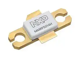
- Transistor Case Style: NI-360H-2SB
- Operating Frequency Max: 2.7GHz
- Operating Frequency Min: 1MHz
- Drain Source Voltage Vds: 125V
- Operating Temperature Max: 225°C
- Continuous Drain Current Id: -
| Delivery and price | |
|---|---|
| Units per pack | 1 |
| Price | 599.0 € |
| Current stock | 10+ |
| Lead time | 30 days |
**NXP Semiconductors** Technical Data Document Number: MMRF5014H Rev. 3, 05/2018 **MMRF5014H** oS **1–2700 MHz, 125 W CW, 50 V WIDEBAND RF POWER GaN TRANSISTOR** a ## **RF Power GaN Transistor** This 125 W CW RF power transistor is optimized for wideband operation up to 2700 MHz and includes input matching for extended bandwidth performance. With its high gain and high ruggedness, this device is ideally suited for CW, pulse and wideband RF applications. This part is characterized and performance is guaranteed for applications operating in the 1–2700 MHz band. There is no guarantee of performance when this part is used in applications designed outside of these frequencies. ## **Typical Narrowband Performance:** VDD = 50 Vdc, IDQ = 350 mA, TA = 25C |**Typical Narrowband Performance:**VDD = 50 Vdc, IDQ = 350 mA, TA = 25CDD = 50 Vdc, IDQ = 350 mA, TA = 25C= 50 Vdc, IDQ = 350 mA, TA = 25CDQ = 350 mA, TA = 25C= 350 mA, TA = 25CA = 25C= 25CCC<br>a|**Typical Narrowband Performance:**VDD = 50 Vdc, IDQ = 350 mA, TA = 25CDD = 50 Vdc, IDQ = 350 mA, TA = 25C= 50 Vdc, IDQ = 350 mA, TA = 25CDQ = 350 mA, TA = 25C= 350 mA, TA = 25CA = 25C= 25CCC<br>a|**Typical Narrowband Performance:**VDD = 50 Vdc, IDQ = 350 mA, TA = 25CDD = 50 Vdc, IDQ = 350 mA, TA = 25C= 50 Vdc, IDQ = 350 mA, TA = 25CDQ = 350 mA, TA = 25C= 350 mA, TA = 25CA = 25C= 25CCC<br>a|a|a| |---|---|---|---|---| |**Typical Narrowband Performance:** VDD = 50 Vdc, IDQ = 350 mA, TA = 25CDD = 50 Vdc, IDQ = 350 mA, TA = 25C= 50 Vdc, IDQ = 350 mA, TA = 25CDQ = 350 mA, TA = 25C= 350 mA, TA = 25CA = 25C= 25CCC<br>**Frequency**<br>**(MHz)**<br>**Signal Type**<br>**Pout**<br>**(W)**<br>**Gps**<br>**(dB)**<br>**D**<br>**(%)**<br>2500 **(1)**<br>CW<br>125 CW<br>16.0<br>64.2<br>2500 **(1)**<br>Pulse<br>(100sec,<br>20% Duty Cycle)<br>125 Peak<br>18.0<br>66.8<br>**Typical Wideband Performance:** VDD= 50 Vdc, TA= 25C<br>**Frequency**<br>**(MHz)**<br>**Signal Type**<br>**Pout**<br>**(W)**<br>**Gps (2)**<br>**(dB)**<br>**D (2)**<br>**(%)**<br>~~SHES]~~||||**NI--360H--2SB**<br> #| |200–2500 **(3)**<br>CW<br>100 CW<br>12.0<br>40.0||||| |1300–1900 **(4)**<br>CW<br>125 CW<br>14.5<br>45.0||Gate|2|| ## **NI--360H--2SB** **==> picture [149 x 108] intentionally omitted <==** **----- Start of picture text -----**<br> Gate 2 1 Drain<br>(Top View)<br>Note: The backside of the package is the<br>source terminal for the transistor.<br>Figure 1. Pin Connections<br>**----- End of picture text -----**<br> |**Load Mismatch/Ruggedness**|| |---|---| |**Frequency**<br>**(MHz)**<br>**Signal Type**<br>**VSWR**<br>**Pin**<br>**(W)**<br>**Test**<br>**Voltage**<br>**Result**<br>2500 **(1)**<br>Pulse<br>(100sec,<br>20% Duty Cycle)<br>> 20:1 at<br>All Phase<br>Angles<br>5.0 Peak<br>(3 dB<br>Overdrive)<br>50<br>No Device<br>Degradation<br>~~FEE~~|| |1. Measured in 2500 MHz narrowband test circuit.|| |2. The values shown are the minimum measured performance numbers across the|The values shown are the minimum measured performance numbers across the| |indicated frequency range.|| 3. Measured in 200–2500 MHz broadband reference circuit. 4. Measured in 1300–1900 MHz broadband reference circuit. ## **Features** - Advanced GaN on SiC, offering high power density - Decade bandwidth performance - Low thermal resistance - Input matched for extended wideband performance - High ruggedness: > 20:1 VSWR ## **Typical Applications** - Ideal for military end--use applications, including the following: - Also suitable for commercial applications, including the following: - Narrowband and multi--octave wideband amplifiers - Public mobile radios, including emergency service radios - Radar - Industrial, scientific and medical - Jammers Jammers – Wideband laboratory amplifiers – EMC testing – Wireless cellular infrastructure 2015, 2017–2018 NXP B.V. **MMRF5014H** RF Device Data ~~—_———~~ NXP Semiconductors ~~NX P~~ 1 **Table 1. Maximum Ratings** |**Table 1. Maximum Ratings**|**Table 1. Maximum Ratings**||||| |---|---|---|---|---|---| |**Rating**||**Symbol**|**Value**||**Unit**| |Drain--Source Voltage||VDSS|125||Vdc| |Gate--Source Voltage||VGS|–8, 0||Vdc| |Operating Voltage||VDD|0 to +50||Vdc| |Maximum Forward Gate Current @ TC= 25C||IGMAX|18||mA| |Storage Temperature Range||Tstg|–65 to +150||C| |Case Operating Temperature Range||TC|–55 to +150||C| |Operating Junction Temperature Range||TJ|–55 to +225||C| |Absolute Maximum Channel Temperature **(1)**||TMAX|350||C| |Total Device Dissipation @ TC= 25C<br>Derate above 25C||PD|232<br>1.16||W<br>W/C| |**Table 2. Thermal Characteristics**|||||| |**Characteristic**||**Symbol**|**Value**||**Unit**| |Thermal Resistance by Infrared Measurement, Active Die Surface--to--Case<br>CW: Case Temperature 82C, 125 W CW, 50 Vdc, IDQ= 350 mA, 2500 MHz||RJC(IR)|0.86 **(2)**||C/W| |Thermal Resistance by Finite Element Analysis, Channel--to--Case<br>Case Temperature 85C, PD= 85 W||RCHC<br>(FEA)|1.48 **(3)**||C/W| |Thermal Impedance by Infrared Measurement, Junction--to--Case<br>Pulse: Case Temperature 58C, 125 W Peak, 100sec Pulse Width,<br>20% Duty Cycle, 50 Vdc, IDQ= 350 mA, 2500 MHz||ZJC(IR)|0.21||C/W| |**Table 3. ESD Protection Characteristics**|||||| |**Test Methodology**|||**Class**||| |Human Body Model (per JESD22--A114)|||1B, passes 500 V||| |Machine Model (per EIA/JESD22--A115)|||A, passes 100 V||| |Charge Device Model (per JESD22--C101)|||IV, passes 2000 V||| |**Table 4. Electrical Characteristics** (TA= 25C unless otherwise noted)|||||| |**Characteristic**|**Symbol**|**Min**|**Typ**|**Max**|**Unit**| |**Off Characteristics**|||||| |Drain Leakage Current<br>(VGS= –8 Vdc, VDS= 10 Vdc)|IDSS|—|—|5|mAdc| |Drain--Source Breakdown Voltage<br>(VGS= –8 Vdc, ID= 25 mAdc)|V(BR)DSS|150|—|—|Vdc| |**On Characteristics**|||||| |Gate Threshold Voltage<br>(VDS= 10 Vdc, ID= 25 mAdc)|VGS(th)|–3.8|–2.9|–2.3|Vdc| |Gate Quiescent Voltage<br>(VDS= 50 Vdc, ID= 350 mAdc, Measured in Functional Test)|VGS(Q)|–3.2|–2.7|–2.2|Vdc| |**Dynamic Characteristics**|||||| |Reverse Transfer Capacitance<br>(VDS= 50 Vdc30 mV(rms)ac @ 1 MHz, VGS= –4 Vdc)|Crss|—|1.0|—|pF| |Output Capacitance<br>(VDS= 50 Vdc30 mV(rms)ac @ 1 MHz, VGS= –4 Vdc)|Coss|—|7.7|—|pF| |Input Capacitance **(4)**<br>(VDS= 50 Vdc, VGS= –4 Vdc30 mV(rms)ac @ 1 MHz)|Ciss|—|51.0|—|pF| 1. Reliability tests were conducted at 225C. Operation with TMAX at 350C will reduce median time to failure. 2. Refer to AN1955, _Thermal Measurement Methodology of RF Power Amplifiers._ Go to http://www.nxp.com/RF and search for AN1955. 3. RJC (FEA) must be used for purposes related to reliability and limitations on maximum junction temperature. MTTF may be estimated by the expression MTTF (hours) = 10[[A + B/(T + 273)]] , where _T_ is the junction temperature in degrees Celsius, _A_ = –8.44 and _B_ = 7210. 4. Part internally input matched. (continued) **MMRF5014H** RF Device Data NXP Semiconductors 2 **Table 4. Electrical Characteristics** (TA = 25C unless otherwise noted) **(continued)** |**Characteristic**|**Characteristic**|**Characteristic**|**Characteristic**|**Characteristic**|**Symbol**|**Min**|**Min**|**Typ**|**Typ**|**Max**|**Unit**| |---|---|---|---|---|---|---|---|---|---|---|---| |**Functional Tests**(In NXP Test Fixture, 50 ohm system) VDD= 50 Vdc, IDQ= 350 mA, Pout= 125 W Peak (25 W Avg.), f = 2500 MHz, 100<br>sec Pulse Width, 20% Duty Cycle.**[See note on correct biasing sequence.]**|||||||||||| |Power Gain|||||Gps|17.0||18.0||20.0|dB| |Drain Efficiency|||||D|64.3||66.8||—|%| |Input Return Loss|||||IRL|—||–12||–9|dB| |**Load Mismatch/Ruggedness**(In NXP Test Fixture, 50 ohm system) IDQ= 350 mA|||||||||||| |**Frequency**<br>**(MHz)**|**Signal Type**||**VSWR**|**Pin**<br>**(W)**||**Test Voltage, VDD**||||**Result**|| |2500|Pulse<br>(100sec,<br>20% Duty Cycle)||> 20:1 at All Phase Angles|5.0 Peak<br>(3 dB Overdrive)|||50||No Device Degradation||| |**Table 5. Ordering Information**|||||||||||| |**Device**||**Tape and Reel Information**|||||||**Package**||| |MMRF5014HR5||R5 Suffix = 50 Units, 32 mm Tape Width, 13--inch Reel|||||NI--360H--2SB||||| ## **NOTE: Correct Biasing Sequence for GaN Depletion Mode Transistors** ## **Turning the device ON** 1. Set VGS to –5 V 2. Turn on VDS to nominal supply voltage (50 V) 3. Increase VGS until IDS current is attained 4. Apply RF input power to desired level ## **Turning the device OFF** 1. Turn RF power off 2. Reduce VGS down to –5 V 3. Reduce VDS down to 0 V (Adequate time must be allowed for VDS to reduce to 0 V to prevent severe damage to device.) 4. Turn off VGS **MMRF5014H** RF Device Data NXP Semiconductors 3 ## **500–2500 MHz WIDEBAND REFERENCE CIRCUIT — 2.0** **4.0** **(5.1 cm** **10.2 cm)** **==> picture [450 x 225] intentionally omitted <==** **----- Start of picture text -----**<br> C9<br>C7*C8*<br>C6<br>L2<br>C2*<br>L1<br>Q1<br>C1*<br>C12*<br>C10* C11*<br>C13* C16*<br>R4 R5<br>C14* C15*<br>C4*<br>C5*<br>C3 R3 MMRF5014H D77847<br>Rev. 0<br>R2<br>R1 + D1<br>**----- End of picture text -----**<br> > *C1, C2, C4, C5, C7, C8, C10, C11, C12, C13, C14, C15 and C16 are mounted vertically. **Figure 2. MMRF5014H Wideband Reference Circuit Component Layout — 500–2500 MHz** **Table 6. MMRF5014H Wideband Reference Circuit Component Designations and Values — 500–2500 MHz** |**Part**|**Description**|**Part Number**|**Manufacturer**| |---|---|---|---| |C1, C5, C7|33 pF Chip Capacitors|ATC800B330JT500XT|ATC| |C2|0.4 pF Chip Capacitor|ATC800B0R4BT500XT|ATC| |C3|2.2F, 16 V Tantalum Capacitor|T491A225K016AT|Kemet| |C4, C8|1000 pF Chip Capacitors|ATC800B102JT50XT|ATC| |C6|220F, 50 V Electrolytic Capacitor|EEV-HA1H221P|Panasonic-ECG| |C9|2.2F Chip Capacitor|HMK432B7225KM-T|Taiyo Yuden| |C10, C11|0.8 pF Chip Capacitors|ATC800B0R8BT500XT|ATC| |C12, C13|9.1 pF Chip Capacitors|ATC800B9R1BT500XT|ATC| |C14, C16|0.5 pF Chip Capacitors|ATC800B0R5BT500XT|ATC| |C15|0.2 pF Chip Capacitor|ATC800B0R2BT500XT|ATC| |D1|LED Green Diffused 1206, SMD|LGN971-KN-1|OSRAM| |L1|33 nH Inductor|1812SMS-33NJLC|Coilcraft| |L2|17.5 nH Inductor, 5 Turns|GA3095-ALC|Coilcraft| |Q1|RF Power GaN Transistor|MMRF5014H|NXP| |R1|75, 1/4 W Chip Resistor|CRCW120675R0FKEA|Vishay| |R2|500Trimming Potentiometer, 11 Turns|3224W-1-501E|Bourns| |R3|470, 1/4 W Chip Resistor|CRCW1206470RFKEA|Vishay| |R4, R5|39, 1/4 W Chip Resistors|CRCW120639R0FKEA|Vishay| |PCB|Rogers RO4350B 0.030,r= 3.66|D77847|MTL| Note: Refer to MMRF5014H’s printed circuit boards and schematics to download the 500–2500 MHz heatsink drawing. **MMRF5014H** RF Device Data NXP Semiconductors 4 ## **TYPICAL CHARACTERISTICS — 500–2500 MHz WIDEBAND REFERENCE CIRCUIT** **==> picture [253 x 175] intentionally omitted <==** **----- Start of picture text -----**<br> 22 70<br>21 VDD = 50 Vdc, IDQ = 300 mA, CW 65<br>20 60<br>19 55<br>100 W D<br>18 50<br>17 45<br>16 40<br>15 35<br>14 10 W Gps 30<br>13 25<br>12 20<br>100 W<br>11 15<br>10 10<br>400 600 800 1000 1200 1400 1600 1800 2000 2200 2400 2600<br>f, FREQUENCY (MHz)<br>, POWER GAIN (dB)<br>ps<br>G DRAIN EFFICIENCY (%)<br>D,<br><br>**----- End of picture text -----**<br> **Figure 3. 500–2500 MHz Wideband Circuit Performance** **MMRF5014H** RF Device Data NXP Semiconductors 5 ## **200–2500 MHz WIDEBAND REFERENCE CIRCUIT — 4.0** **5.0** **(10.2 cm** **12.7 cm)** **==> picture [502 x 565] intentionally omitted <==** **----- Start of picture text -----**<br> Section AA<br>MMRF5014H<br>Rev. 6<br>D68303<br>R1** T2<br>T2<br>C17* B1 T2 B2 B1<br>C2* C3* Q1 C16*<br>C1**<br>L2 C15* T1<br>R3 R4 C13* T1 See<br>R2**<br>Detail BB<br>L1 C12*<br>C6* C11<br>C5<br>VDD<br>C4 C7 C8 C9 C10<br>C14<br>VGG<br>**C1, C2, C3, C6, C12, C13, C15, C16, C17, R1, and R2 are mounted vertically.<br>**Stacked Section AA<br>C17* T2<br>B1 B2<br>C16*<br>C15*<br>T1<br>Detail BB 2X<br>**----- End of picture text -----**<br> **Figure 4. MMRF5014H Wideband Reference Circuit Component Layout — 200–2500 MHz** **MMRF5014H** RF Device Data NXP Semiconductors 6 **Table 7. MMRF5014H Wideband Reference Circuit Component Designations and Values — 200–2500 MHz** |**Part**|**Description**|**Part Number**|**Manufacturer**| |---|---|---|---| |B1, B2|Ferrite Beads|T22-6|Micro Metals| |C1|56 pF Chip Capacitor|ATC800B560JT500XT|ATC| |C2|75 pF Chip Capacitor|ATC800B750JT500XT|ATC| |C3|1.6 pF Chip Capacitor|ATC800B1R6BT500XT|ATC| |C4|6.8F Chip Capacitor|C4532X7R1H685K|TDK| |C5, C8, C9, C11|0.015F Chip Capacitors|GRM319R72A153KA01D|Murata| |C6, C12|5.6 pF Chip Capacitors|ATC800B5R6BT500XT|ATC| |C7, C10|1F Chip Capacitors|GRM31CR72A105KAO1L|Murata| |C13|1.4 pF Chip Capacitor|ATC800B1R4BT500XT|ATC| |C14|220F, 100 V Electrolytic Capacitor|EEV-FK2A221M|Panasonic-ECG| |C15, C17|0.9 pF Chip Capacitors|ATC800B0R9BT500XT|ATC| |C16|47 pF Chip Capacitor|ATC800B470JT500XT|ATC| |L1|12.5 nH Inductor, 4 Turns|A04TJLC|Coilcraft| |L2|22 nH Inductor|1812SMS-22NJLC|Coilcraft| |Q1|RF Power GaN Transistor|MMRF5014H|NXP| |R1, R2|10, 3/4 W Chip Resistors|CRCW201010R0FKEF|Vishay| |R3, R4|39, 1/4 W Chip Resistors|CRCW120639R0FKEA|Vishay| |T1|25Semi Rigid Coax, 0.770Shield Length|UT-070-25|Micro--Coax| |T2|25Semi Rigid Coax, 0.850Shield Length|UT-070-25|Micro--Coax| |PCB|Rogers RO4350B, 0.030,r= 3.66|D68303|MTL| Note: Refer to MMRF5014H’s printed circuit boards and schematics to download the 200–2500 MHz heatsink drawing. **MMRF5014H** RF Device Data NXP Semiconductors 7 ## **TYPICAL CHARACTERISTICS — 200–2500 MHz WIDEBAND REFERENCE CIRCUIT** **==> picture [253 x 175] intentionally omitted <==** **----- Start of picture text -----**<br> 23 70<br>22 VDD = 50 Vdc, IDQ = 350 mA, CW 65<br>21 60<br>20 55<br>100 W<br>19 D 50<br>18 45<br>17 40<br>16 35<br>15 10 W Gps 30<br>14 25<br>13 20<br>100 W<br>12 15<br>11 10<br>200 600 1000 1400 1800 2200 2600<br>f, FREQUENCY (MHz)<br>, POWER GAIN (dB)<br>ps<br>G DRAIN EFFICIENCY (%)<br>D,<br><br>**----- End of picture text -----**<br> **Figure 5. 200–2500 MHz Wideband Circuit Performance** **MMRF5014H** RF Device Data NXP Semiconductors 8 ## **TYPICAL CHARACTERISTICS — OPTIMIZED NARROWBAND PERFORMANCE** ## **Narrowband Performance and Impedance Information** (TC = 25C) The measured input and output impedances are presented to the input of the device at the package reference plane. Measurements are performed in NXP narrowband fixture tuned at 500, 1000, 1500, 2000 and 2500 MHz. **==> picture [275 x 458] intentionally omitted <==** **----- Start of picture text -----**<br> 32 80<br>VDD = 50 Vdc, IDQ = 300 mA, CW 1000 MHz<br>30 500 MHz 72<br>2500 MHz<br>28 64<br>500 MHz<br>26 56<br>2000 MHz<br>24 48<br>D<br>1500 MHz<br>22 40<br>20 1500 MHz 1000 MHz 32<br>18 2500 MHz G ps 24<br>16 16<br>2000 MHz<br>14 8<br>12 0<br>0 20 40 60 80 100 120 140 160 180 200<br>Pout, OUTPUT POWER (WATTS)<br>Figure 6. Power Gain and Drain Efficiency<br>versus CW Output Power<br>f Zsource Zload<br>MHz <br>500 1.3 + j3.9 5.9 + j3.5<br>1000 1.0 + j0.3 5.5 + j2.9<br>1500 0.8 – j0.5 3.4 + j2.0<br>2000 1.2 – j2.0 4.7 + j0.3<br>2500 2.7 – j3.8 3.7 + j1.4<br>Zsource = Test circuit impedance as measured<br>from gate to ground.<br>Zload = Test circuit impedance as measured<br>from drain to ground.<br>Input Device Output<br>Matching Under Matching<br>Network Test Network<br>50 50 <br>Zsource Zload<br>, POWER GAIN (dB)<br>ps<br>G DRAIN EFFICIENCY (%)<br>D,<br><br>**----- End of picture text -----**<br> **Figure 7. Narrowband Fixtures: Series Equivalent Source and Load Impedances** **MMRF5014H** RF Device Data NXP Semiconductors 9 ## **1300–1900 MHz WIDEBAND REFERENCE CIRCUIT — 2.0** **3.0** **(5.1 cm** **7.6 cm)** |**Figure 8. MMRF5014H Wideband Reference Circuit Component Layout — 1300–1900 MHz**<br>*C9 is mounted vertically.<br>MMRF5014H<br>Rev. 1<br>VGG<br>VDD<br>D67114<br>C9*<br>R1<br>R2<br>R3<br>R4 R5<br>C1<br>C2 C3 C4<br>C5 C6 C7<br>C8<br>Q1<br>L1<br>L2<br>D1<br>**Table 8. MMRF5014H Wideband Reference Circuit Component Designations and Values — 1300–1900 MHz**|**Figure 8. MMRF5014H Wideband Reference Circuit Component Layout — 1300–1900 MHz**<br>*C9 is mounted vertically.<br>MMRF5014H<br>Rev. 1<br>VGG<br>VDD<br>D67114<br>C9*<br>R1<br>R2<br>R3<br>R4 R5<br>C1<br>C2 C3 C4<br>C5 C6 C7<br>C8<br>Q1<br>L1<br>L2<br>D1<br>**Table 8. MMRF5014H Wideband Reference Circuit Component Designations and Values — 1300–1900 MHz**|**Figure 8. MMRF5014H Wideband Reference Circuit Component Layout — 1300–1900 MHz**<br>*C9 is mounted vertically.<br>MMRF5014H<br>Rev. 1<br>VGG<br>VDD<br>D67114<br>C9*<br>R1<br>R2<br>R3<br>R4 R5<br>C1<br>C2 C3 C4<br>C5 C6 C7<br>C8<br>Q1<br>L1<br>L2<br>D1<br>**Table 8. MMRF5014H Wideband Reference Circuit Component Designations and Values — 1300–1900 MHz**|**Figure 8. MMRF5014H Wideband Reference Circuit Component Layout — 1300–1900 MHz**<br>*C9 is mounted vertically.<br>MMRF5014H<br>Rev. 1<br>VGG<br>VDD<br>D67114<br>C9*<br>R1<br>R2<br>R3<br>R4 R5<br>C1<br>C2 C3 C4<br>C5 C6 C7<br>C8<br>Q1<br>L1<br>L2<br>D1<br>**Table 8. MMRF5014H Wideband Reference Circuit Component Designations and Values — 1300–1900 MHz**| |---|---|---|---| |**Part**|**Description**|**Part Number**|**Manufacturer**| |C1|18 pF Chip Capacitor|ATC600S180CT250XT|ATC| |C2|2.2F Tantalum Capacitor|T491A225K016AT|Kemet| |C3, C6|1000 pF Chip Capacitors|ATC800B102JT50XT|ATC| |C4, C5|33 pF Chip Capacitors|ATC800B330JT500XT|ATC| |C7|2.2F Chip Capacitor|HMK432B7225KM-T|Taiyo Tuden| |C8|47F, 100 V Electrolytic Capacitor|476KXM050M|Panasonic-ECG| |C9|9.1 pF Chip Capacitor|ATC800B9R1BT500XT|ATC| |D1|LED Green Diffused 1206, SMD|LGN971--KN--1|OSRAM| |Q1|RF Power GaN Transistor|MMRF5014H|NXP| |R1|75, 1/4 W Chip Resistor|CRCW120675R0FKEA|Vishay| |R2|5 kTrimming Potentiometer, 11 Turns|3224W-1-502E|Bourns| |R3|5 k, 1/4 W Chip Resistor|CRCW12065K00FKEA|Vishay| |R4, R5|39, 1/4 W Chip Resistors|CRCW120639R0FKEA|Vishay| |L1, L2|33 nH Inductors|1812SMS-33NJLC|Coilcraft| |PCB|Rogers 3010, 0.025,r= 10.2|D67114|MTL| **MMRF5014H** RF Device Data NXP Semiconductors 10 ## **TYPICAL CHARACTERISTICS — 1300–1900 MHz WIDEBAND REFERENCE CIRCUIT** **==> picture [253 x 394] intentionally omitted <==** **----- Start of picture text -----**<br> 30 70<br>VDD = 50 Vdc, IDQ = 200 mA, Pout = 125 W, CW<br>28 66<br>26 62<br>24 58<br>D<br>22 54<br>20 50<br>18 46<br>16 Gps 42<br>14 38<br>12 34<br>10 30<br>1300 1400 1500 1600 1700 1800 1900<br>f, FREQUENCY (MHz)<br>Figure 9. Power Gain and Drain Efficiency<br>versus Frequency<br>20 75<br>VDD = 50 Vdc, IDQ = 200 mA, CW<br>18 70<br>1900 MHz<br>16 65<br>1600 MHz<br>14 Gps 1300 MHz 60<br>12 1900 MHz 55<br>1600 MHz<br>10 50<br>1300 MHz<br>8 45<br>D<br>6 40<br>4 35<br>2 30<br>0 25<br>0 20 40 60 80 100 120 140 160 180<br>Pout, OUTPUT POWER (WATTS)<br>, POWER GAIN (dB)<br>ps<br>G DRAIN EFFICIENCY (%)<br>D,<br><br>, POWER GAIN (dB)<br>ps<br>G DRAIN EFFICIENCY (%)<br>D,<br><br>**----- End of picture text -----**<br> **Figure 10. Power Gain and Drain Efficiency versus CW Output Power** **MMRF5014H** RF Device Data NXP Semiconductors 11 **2500 MHz NARROWBAND PRODUCTION TEST FIXTURE — 4.0** **5.0** **(10.2 cm** **12.7 cm)** **==> picture [394 x 316] intentionally omitted <==** **----- Start of picture text -----**<br> VGG VDD<br>D65152<br>C8 C12<br>R2<br>C14 C7<br>C10<br>C2 C3<br>C4 C5 C9<br>C13<br>R1<br>C1 C6<br>C11<br>MMRF5014H<br>Rev. 4<br>CUT OUT AREA<br>**----- End of picture text -----**<br> **Figure 11. MMRF5014H Narrowband Test Circuit Component Layout — 2500 MHz** **Table 9. MMRF5014H Narrowband Test Circuit Component Designations and Values — 2500 MHz** |**Part**|**Description**|**Part Number**|**Manufacturer**| |---|---|---|---| |C1<br>3.|9 pF Chip Capacitor|ATC600F3R9BT250XT|ATC| |C2, C3, C4, C5, C6<br>12|pF Chip Capacitors|ATC600F120JT250XT|ATC| |C7, C14<br>4.|7F Chip Capacitors|C4532X7R1H475K200KB|TDK| |C8<br>0.|1F Chip Capacitor|GRM319R72A104KA01D|Murata| |C9<br>1.|0F Chip Capacitor|GRM32CR72A105KA35L|Murata| |C10<br>22|0F, 100 V Electrolytic Capacitor|EEV-FK2A221M|Panasonic-ECG| |C11<br>1|pF Chip Capacitor|ATC600F1R0BT250XT|ATC| |C12, C13<br>10|00 pF Chip Capacitors|ATC800B102JT50XT|ATC| |R1<br>56|, 1/4 W Chip Resistor|CRCW120656R0FKEA|Vishay| |R2<br>0|, 5 A Chip Resistor|CRCW12100000Z0EA|Vishay| |PCB<br>R|ogers RO4350B, 0.030,r= 3.66|D65152|MTL| **MMRF5014H** RF Device Data NXP Semiconductors 12 **==> picture [487 x 174] intentionally omitted <==** **----- Start of picture text -----**<br> Z9 Z8 Z16 Z17 R2<br>VBIAS VSUPPLY<br>+<br>C14 C7 C8 C12 C2 C3 C4 C5 C13 C9 C10<br>Z7<br>Z15<br>R1<br>RF Z6 RF<br>INPUT OUTPUT<br>Z1 Z2 Z3 Z4 Z5 Z10 Z11 Z12 Z13 Z14<br>C1 C6<br>C11<br>DUT<br>**----- End of picture text -----**<br> **Figure 12. MMRF5014H Narrowband Test Circuit Schematic — 2500 MHz** **Table 10. MMRF5014H Narrowband Test Circuit Microstrips — 2500 MHz** |**Microstrip**|**Description**||**Microstrip**|**Description**| |---|---|---|---|---| |Z1|1.8700.064Microstrip||Z10|0.1450.515Microstrip| |Z2, Z3|0.0300.070Microstrip||Z11|0.3530.515Microstrip| |Z4|0.1050.525Microstrip||Z12|0.0400.064Microstrip| |Z5*|0.2400.525Microstrip||Z13|0.6870.064Microstrip| |Z6|0.0370.050Microstrip||Z14|1.0200.064Microstrip| |Z7|0.4650.050Microstrip||Z15|0.4680.050Microstrip| |Z8|0.0900.050Microstrip||Z16|0.1580.050Microstrip| |Z9|0.1900.050Microstrip||Z17|0.0780.050Microstrip| * Line length include microstrip bends **MMRF5014H** RF Device Data NXP Semiconductors 13 ## **TYPICAL CHARACTERISTICS — 2500 MHz** **==> picture [503 x 416] intentionally omitted <==** **----- Start of picture text -----**<br> 22 70<br>21 I DQ = 350 mA, f = 2500 MHz 45 V 50 V<br>2019 Pulse Width = 100Duty Cycle = 20% sec 60 30 V 35 V 40 V<br>VDD = 25 V<br>18<br>50<br>17<br>16<br>40<br>15<br>50 V<br>14 45 V<br>13 40 V 30<br>12 35 V IDQ = 350 mA, f = 2500 MHz<br>11 30 V 20 Pulse Width = 100 sec<br>10 VDD = 25 V Duty Cycle = 20%<br>9 10<br>10 30 50 70 90 110 130 150 170 190 0 20 40 60 80 100 120 140 160 180<br>Pout, OUTPUT POWER (WATTS) PEAK Pout, OUTPUT POWER (WATTS) PEAK<br>Figure 13. Power Gain versus Output Power Figure 14. Drain Efficiency versus Output Power<br>and Drain Voltage [(1)] and Drain Voltage [(1)]<br>180 22 70<br>TC = –55 _ C D<br>160<br>140 –55C TC = 25C 21 –55 _ C 85 _ C 60<br>120 85C 20 25 _ C 25 _ C 50<br>100 19 85 _ C 40<br>80 18 30<br>60 Gps<br>17 20<br>40<br>IDQ = 350 mA, f = 2500 MHz<br>20 VDD = 50 Vdc, IDQ = 350 mA, f = 2500 MHz 16 Pulse Width = 100 sec 10<br>Pulse Width = 100 sec, Duty Cycle = 20%<br>Duty Cycle = 20%<br>0 15 0<br>0 1 2 3 4 5 6 0 20 40 60 80 100 120 140 160 180 200<br>Pin, INPUT POWER (WATTS) PEAK Pout, OUTPUT POWER (WATTS) PEAK<br>Figure 15. Output Power versus Input Power [(1)] Figure 16. Power Gain and Drain Efficiency<br>versus Output Power [(1)]<br>, POWER GAIN (dB)<br>ps<br>G , DRAIN EFFICIENCY (%)D<br><br>, POWER GAIN (dB)<br>ps<br>G DRAIN EFFICIENCY (%)<br>D,<br>, OUTPUT POWER (WATTS) PEAK <br>out<br>P<br>**----- End of picture text -----**<br> ## **1. Circuit tuned for maximum power.** **MMRF5014H** RF Device Data NXP Semiconductors 14 ## **PACKAGE DIMENSIONS** Pin 1. Drain 2. Gate 3. Source **MMRF5014H** RF Device Data NXP Semiconductors 15 **MMRF5014H** RF Device Data NXP Semiconductors 16 ## **PRODUCT DOCUMENTATION AND TOOLS** Refer to the following resources to aid your design process. ## **Application Notes** - AN1955: Thermal Measurement Methodology of RF Power Amplifiers ## **Development Tools** - Printed Circuit Boards ## **To Download Resources Specific to a Given Part Number:** 1. Go to http://www.nxp.com/RF 2. Search by part number 3. Click part number link 4. Choose the desired resource from the drop down menu ## **REVISION HISTORY** The following table summarizes revisions to this document. |**Revision**|**Date**|**Description**| |---|---|---| |0|May 2015|<br>Initial Release of Data Sheet| |1|Sept. 2015|<br>Table 1, Maximum Ratings: added Maximum Forward Gate Current, p. 2<br><br>Table 4, Electrical Characteristics: changed Load Mismatch/Ruggedness signal type to pulse to reflect<br>correct modulation signal, p. 3| |2|Apr. 2017|<br>Biasing sequence for GaN depletion mode transistors: revised note to clarify correct biasing sequence for<br>GaN parts, p. 3<br><br>500–2500 MHz wideband reference circuit: added performance data and graph, reference circuit<br>component layout and component designations, pp. 4–5| |3|May 2018|<br>Table 2, Thermal Characteristics: updated to include RCHC(FEA) data, p. 2| **MMRF5014H** RF Device Data NXP Semiconductors 17 ## _**How to Reach Us:**_ **Home Page:** nxp.com **Web Support:** nxp.com/support Information in this document is provided solely to enable system and software implementers to use NXP products. There are no express or implied copyright licenses granted hereunder to design or fabricate any integrated circuits based on the information in this document. NXP reserves the right to make changes without further notice to any products herein. NXP makes no warranty, representation, or guarantee regarding the suitability of its products for any particular purpose, nor does NXP assume any liability arising out of the application or use of any product or circuit, and specifically disclaims any and all liability, including without limitation consequential or incidental damages. “Typical” parameters that may be provided in NXP data sheets and/or specifications can and do vary in different applications, and actual performance may vary over time. All operating parameters, including “typicals,” must be validated for each customer application by customer’s technical experts. NXP does not convey any license under its patent rights nor the rights of others. NXP sells products pursuant to standard terms and conditions of sale, which can be found at the following address: nxp.com/SalesTermsandConditions. NXP, the NXP logo, Freescale, and the Freescale logo are trademarks of NXP B.V. All other product or service names are the property of their respective owners. E 2015, 2017–2018 NXP B.V. ## **MMRF5014H** RF Device Data NXP Semiconductors Document Number: MMRF5014H 18Rev. 3, 05/2018
Updated at April 10, 2026
NXP Semiconductors is a global leader in secure connectivity solutions, driving innovation across the automotive, industrial, IoT, mobile, and communications infrastructure markets. By developing advanced, purpose-built technologies, NXP enables devices to sense, think, connect, and act intelligently, delivering rigorously tested components that make the connected world safer and more efficient. Within the semiconductor space, NXP is highly regarded for its extensive range of high-performance integrated circuits and discrete devices. The brand's portfolio excels in drivers and interfaces, featuring a comprehensive selection of I/O expanders designed to streamline complex system architectures. For demanding high-frequency and wireless applications, NXP provides industry-leading RF FETs and RF/PIN diodes engineered to deliver exceptional signal integrity, efficiency, and reliability. The NXP product lineup further extends to essential discrete components, including versatile bipolar transistors, JFETs, and small signal diodes optimized for precision switching and amplification. Additionally, the portfolio supports advanced automation and smart applications with precision IC sensors, such as MEMS accelerometers, alongside specialized power management solutions like AC/DC LED driver ICs and single MOSFETs for cutting-edge electronics design.
About Novapart
Novapart is a B2B electronic component broker specialising in stock shortages and cost reduction. We source hard-to-find parts and identify compliant alternatives across a catalogue of 410,000+ components from 500+ manufacturers.
Learn more →Stock Shortage Specialist
When a component is unavailable, discontinued or has an unacceptable lead time, we tap into our network of vetted European and Asian distributors to source what you need — without compromising on quality or traceability.
Request a quote →Compliant Alternatives
We identify pin-to-pin, electrically equivalent substitutes that meet the same certifications (RoHS, AEC-Q100, REACH) as your original specification — validated against datasheets, not just part numbers. Often at a lower cost.
BOM Analysis service →