


MMRF1015NR1
RF FET Transistor, 0.27 V, 1 MHz, 2 GHz, TO-270
- Manufacturer: NXP
- Product type: RF FETs
- Drain Source Voltage Vds:0.27V; Continuous Drain Current Id:-; Power Dissipation Pd:-; Operating Frequency Min:1MHz; Operating Frequency Max:2GHz; RF Transistor Case:TO-270; No. of Pins
- MSL: MSL 3 - 168 hours
- SVHC: No SVHC (27-Jun-2024)
- No. of Pins: 2Pins
- Channel Type: N Channel
- Product Range: -
- Power Dissipation: -
- Transistor Mounting: Flange
- Transistor Case Style: TO-270
- Operating Frequency Max: 2GHz
- Operating Frequency Min: 1MHz
- Drain Source Voltage Vds: 0.27V
- Operating Temperature Max: 225°C
- Continuous Drain Current Id: -
| Delivery and price | |
|---|---|
| Units per pack | 100 |
| Price | 17.17 € |
| Current stock | 10+ |
| Lead time | 30 days |
**Freescale Semiconductor**
Document Number: MMRF1015N Rev. 0, 7/2014
Technical Data
## **RF Power LDMOS Transistors**
## N--Channel Enhancement--Mode Lateral MOSFETs
Designed for Class A or Class AB power amplifier applications with frequencies up to 2000 MHz. Suitable for analog and digital modulation and multicarrier amplifier applications.
- Typical Two--Tone Performance at 960 MHz: VDD = 28 Vdc, IDQ = 125 mA, Pout = 10 W PEP Power Gain — 18 dB Drain Efficiency — 32% IMD — --37 dBc
- Capable of Handling 10:1 VSWR @ 28 Vdc, 960 MHz, 10 W CW Output Power
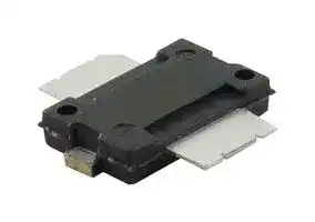
## **MMRF1015NR1 MMRF1015GNR1**
**1--2000 MHz, 10 W, 28 V CLASS A/AB RF POWER MOSFETs**
## **Features**
- Characterized with Series Equivalent Large--Signal Impedance Parameters
- On--Chip RF Feedback for Broadband Stability
- Qualified Up to a Maximum of 32 VDD Operation
- Integrated ESD Protection
**==> picture [59 x 27] intentionally omitted <==**
**----- Start of picture text -----**<br>
TO--270--2<br>PLASTIC<br>MMRF1015NR1<br>**----- End of picture text -----**<br>
- 225C Capable Plastic Package
- In Tape and Reel. R1 Suffix = 500 Units, 24 mm Tape Width, 13--inch Reel.
**==> picture [65 x 27] intentionally omitted <==**
**----- Start of picture text -----**<br>
TO--270G--2<br>PLASTIC<br>MMRF1015GNR1<br>**----- End of picture text -----**<br>
**==> picture [155 x 116] intentionally omitted <==**
**----- Start of picture text -----**<br>
Gate 2 1 Drain<br>e t<br>(Top View)<br>Note: Exposed backside of the package is<br>the source terminal for the transistor.<br>Figure 1. Pin Connections<br>**----- End of picture text -----**<br>
**Table 1. Maximum Ratings**
|**Table 1. Maximum Ratings**|**Table 1. Maximum Ratings**|**Table 1. Maximum Ratings**|**Table 1. Maximum Ratings**|**Table 1. Maximum Ratings**|||e~~t~~|
|---|---|---|---|---|---|---|---|
|**Rating**<br>**Symbol**<br>**Value**<br>**Unit**<br>Drain--Source Voltage<br>VDSS<br>--0.5, +68<br>Vdc<br>Gate--Source Voltage<br>VGS<br>--0.5, +12<br>Vdc<br>Storage Temperature Range<br>Tstg<br>--65 to +150<br>C<br>Case Operating Temperature<br>TC<br>150<br>C<br>Operating Junction Temperature **(1,2)**<br>TJ<br>225<br>C<br>**Table 2. Thermal Characteristics**<br>~~——~~||||||Note:|Exposed backside of the package<br>the source terminal for the transistor.<br>(Top View)<br>**Figure 1. Pin Connections**|
|**Characteristic**|||||**Symbol**||**Value (2,3)**<br>**Unit**|
|Thermal Resistance, Junction to Case|||||RJC||2.85<br>C/W|
|Case Temperature 80C, 10 W PEP||||||||
1. Continuous use at maximum temperature will affect MTTF.
2. MTTF calculator available at http://www.freescale.com/rf. Select Software & Tools/Development Tools/Calculators to access MTTF calculators by product.
3. Refer to AN1955, _Thermal Measurement Methodology of RF Power Amplifiers._ Go to http://www.freescale.com/rf. Select Documentation/Application Notes -- AN1955.
**MMRF1015NR1 MMRF1015GNR1** ~~* freescale~~
Freescale Semiconductor, Inc., 2014. All rights reserved.
RF Device Data Freescale Semiconductor, Inc.
1
|**Table 3. ESD Protection Characteristics**|
|---|
|**Test Methodology**<br>**Class**<br>Human Body Model (per JESD22--A114)<br>1A<br>Machine Model (per EIA/JESD22--A115)<br>A<br>Charge Device Model (per JESD22--C101)<br>III<br>**Table 4. Moisture Sensitivity Level**<br>**Test Methodology**<br>**Rating**<br>**Package Peak Temperature**<br>**Unit**<br>Per JESD22--A113, IPC/JEDEC J--STD--020<br>3<br>260<br>C<br>~~—a~~|
|**Table 5. Electrical Characteristics** (TA= 25C unless otherwise noted)|
|**Characteristic**<br>**Symbol**<br>**Min**<br>**Typ**<br>**Max**<br>**Unit**|
|**Off Characteristics**|
|Zero Gate Voltage Drain Leakage Current<br>(VDS= 68 Vdc, VGS= 0 Vdc)<br>IDSS<br>—<br>—<br>10<br>Adc<br>Zero Gate Voltage Drain Leakage Current<br>(VDS= 28 Vdc, VGS= 0 Vdc)<br>IDSS<br>—<br>—<br>1<br>Adc<br>Gate--Source Leakage Current<br>(VGS= 5 Vdc, VDS= 0 Vdc)<br>IGSS<br>—<br>—<br>1<br>Adc<br>~~—~~|
|**On Characteristics**|
|Gate Threshold Voltage<br>(VDS= 10 Vdc, ID= 100Adc)<br>VGS(th)<br>1.5<br>2.3<br>3<br>Vdc<br>Gate Quiescent Voltage<br>(VDD= 28 Vdc, ID= 125 mAdc, Measured in Functional Test)<br>VGS(Q)<br>2<br>3.1<br>4<br>Vdc<br>Drain--Source On--Voltage<br>(VGS= 10 Vdc, ID= 0.3 Adc)<br>VDS(on)<br>0.15<br>0.27<br>0.35<br>Vdc<br>~~—~~|
|**Dynamic Characteristics**|
|Reverse Transfer Capacitance<br>(VDS= 28 Vdc30 mV(rms)ac @ 1 MHz, VGS= 0 Vdc)<br>Crss<br>—<br>0.32<br>—<br>pF<br>Output Capacitance<br>(VDS= 28 Vdc30 mV(rms)ac @ 1 MHz, VGS= 0 Vdc)<br>Coss<br>—<br>10<br>—<br>pF<br>Input Capacitance<br>(VDS= 28 Vdc, VGS= 0 Vdc30 mV(rms)ac @ 1 MHz)<br>Ciss<br>—<br>23<br>—<br>pF<br>~~—~~|
|**Functional Tests (1)** (In Freescale Test Fixture, 50 ohm system) VDD= 28 Vdc, IDQ= 125 mA, Pout= 10 W PEP, f = 960 MHz, Two--Tone|
|Test, 100 kHz Tone Spacing|
|Power Gain<br>Gps<br>17.5<br>18<br>20.5<br>dB<br>Drain Efficiency<br>D<br>31<br>32<br>—<br>%<br>Intermodulation Distortion<br>IMD<br>—<br>--37<br>--33<br>dBc<br>Input Return Loss<br>IRL<br>—<br>--18<br>--10<br>dB<br>~~———~~|
|**Typical Performance**(In Freescale 450 MHz Demo Board, 50hm system) VDD= 28 Vdc, IDQ= 150 mA, Pout= 10 W PEP, 420--470 MHz,|
|Two--Tone Test, 100 kHz Tone Spacing|
|Power Gain<br>Gps<br>—<br>20<br>—<br>dB<br>Drain Efficiency<br>D<br>—<br>33<br>—<br>%<br>Intermodulation Distortion<br>IMD<br>—<br>--40<br>—<br>dBc<br>Input Return Loss<br>IRL<br>—<br>--10<br>—<br>dB<br>1. Measurements made with device in straight lead configuration before any lead forming operation is applied. Lead forming is used for gull wing<br>(GN) parts.<br>~~—sa~~|
**MMRF1015NR1 MMRF1015GNR1**
RF Device Data Freescale Semiconductor, Inc.
2
**==> picture [419 x 214] intentionally omitted <==**
**----- Start of picture text -----**<br>
B1 C11<br>VBIAS + + + + + VSUPPLY<br>C12<br>C2 C3 C4 C6 C7 C15 C16 C18 C19<br>C10<br>C13<br>L1<br>RF<br>RF R1 DUT Z5 Z6 Z7 OUTPUT<br>INPUT Z1 Z2 Z3 Z4<br>C20<br>C14 C17<br>C1<br>C5 C8 C9<br>eels<br>Z1 0.073 x 0.223 Microstrip Z5 0.313 x 0.902 Microstrip<br>Z2 0.112 x 0.070 Microstrip Z6 0.073 x 1.080 Microstrip<br>Z3 0.213 x 0.500 Microstrip Z7 0.073 x 0.314 Microstrip<br>Z4 0.313 x 1.503 Microstrip PCB Rogers ULTRALAM 2000, 0.031, r = 2.55<br>**----- End of picture text -----**<br>
**Figure 2. MMRF1015NR1 Test Circuit Schematic — 900 MHz**
**Table 6. MMRF1015NR1 Test Circuit Component Designations and Values — 900 MHz**
|**Part**|**Description**|**Part Number**|**Manufacturer**|
|---|---|---|---|
|B1|Ferrite Bead|2743019447|Fair--Rite|
|C1, C6, C11, C20|47 pF Chip Capacitors|ATC100B470JT500XT|ATC|
|C2, C18, C19|22F, 35 V Tantalum Capacitors|T491D226K035AT|Kemet|
|C3, C16|220F, 63 V Electrolytic Capacitors, Radial|2222--136--68221|Vishay|
|C4, C15|0.1F Chip Capacitors|CDR33BX104AKWS|Kemet|
|C5, C8, C17|0.8--8.0 pF Variable Capacitors, Gigatrim|272915L|Johanson|
|C7, C12|24 pF Chip Capacitors|ATC100B240JT500XT|ATC|
|C9, C10, C13|6.8 pF Chip Capacitors|ATC100B6R8JT500XT|ATC|
|C14|7.5 pF Chip Capacitor|ATC100B7R5JT500XT|ATC|
|L1|12.5 nH Inductor|A04T--5|Coilcraft|
|R1|1 k1/4 W ChipResistor|CRCW12061001FKEA|Vishay|
**MMRF1015NR1 MMRF1015GNR1**
RF Device Data Freescale Semiconductor, Inc.
3
**==> picture [461 x 166] intentionally omitted <==**
**----- Start of picture text -----**<br>
C3 C18<br>C7<br>° ceso0/{f _t 4 | ) ° ooavcascoccvvcvcecSS rscccccvcevcene) ProdLA O g°<br>C4<br>° ° of; oO C16 °<br>$ 2000000 Ss °<br>o| [ 3 ° C15 °<br>° + 7 i C10 ([ Te — O°<br>ie}od r©000060 T| 0 C6 _|000000000 ° re)oo00000° 000000000000 lomemene)° oO00000000 Abo °°<br>) C2 B1 ) J};}} 9°° @ @ °3Sia C11 (ToOoo G@) C19 ~ )<br>C13<br>0000000000000 090000000000000 ° Ome)0000 o)coool[Uo|] y 55 C12<br>x & S$<br>R1 7 L1 \ 0000000000000000000000<br>al |<br>C1 E 71 — C9 i] C20<br>0000000000000 2 a Ce nn<br>Po{ | sy tr J° | | C17<br>C14<br>C5 poseoeecoea—pecoossoes C8 00000000000000000<br>**----- End of picture text -----**<br>
**Figure 3. MMRF1015NR1 Test Circuit Component Layout — 900 MHz**
**MMRF1015NR1 MMRF1015GNR1**
RF Device Data Freescale Semiconductor, Inc.
4
**TYPICAL CHARACTERISTICS — 900 MHz**
**==> picture [500 x 648] intentionally omitted <==**
**----- Start of picture text -----**<br>
--8<br>48<br>ee D --10<br>44<br>eae --12<br>40 IRL<br>--14<br>So<br>36<br>VDD = 28 Vdc, Pout = 10 W (Avg.) aa --16<br>32 IDQ = 125 mA, 100 kHz Tone Spacing --18<br>28 a<br>a ee— --20<br>24 IMD<br>ee PT —— e | | eeeJ | --22<br>20 a Gps a --24<br>16<br>ee --26<br>910 920 930 940 950 960 970<br>f, FREQUENCY (MHz)<br>Figure 4. Two--Tone Wideband Performance<br>@ Pout = 10 Watts<br>20 --10<br>IDQ = 190 mA VDD = 28 Vdc, IDQ = 125 mA 3rd Order<br>--20 f = 945 MHz, Two--Tone Measurements<br>19 100 kHz Tone Spacing<br>BPr a et 125 mA m OTFIM EU We y 5th Order<br>--30<br>“i t E T | [IT Ht<br>18 90 mA<br>--40<br>17 si ti A 1 TN aS oHa 7th Order |<br>--50<br>16 VDD = 28 Vdc, f = 945 MHz<br>--60<br>Two--Tone Measurements<br>100 kHz Tone Spacing<br>15 aUTIL ELT --70 Cif a r a, en<br>0.1 1 10 100 0.1 1 10 100<br>Pout, OUTPUT POWER (WATTS) AVG. Pout, OUTPUT POWER (WATTS) AVG.<br>Figure 5. Two--Tone Power Gain versus Figure 6. Intermodulation Distortion Products<br>Output Power versus Output Power<br>--15 48<br>VDD = 28 Vdc, Pout = 10 W (Avg.) Ideal<br>--20 IDQ = 125 mA, Two--Tone Measurements<br>(f1+f2)/2 = Center Frequency = 945 MHz 46 P3dB = 43.14 dBm (20.61 W)<br>S e<br>--25<br>--30 E2! e Da =sana s= 2=<br>Sel l | 44 EE P1dB = 42.23 dBm (16.71 W) E<br>3rd Order<br>--35<br>Actual<br>--40 CO te ry 42 aaeSECR sane<br>--45 ell 5th Order ee a til AA T<br>40 VDD = 28 Vdc, IDQ = 125 mA<br>--50 7th Order Pulsed CW, 8 sec(on), 1 msec(off)<br>--55 er e 38 f = 945 MHz<br>| till |EH ann<br>0.1 1 10 100 19 21 23 25 27 29<br>TWO--TONE SPACING (MHz) Pin, INPUT POWER (dBm)<br>Figure 7. Intermodulation Distortion Products Figure 8. Pulse CW Output Power versus<br>versus Tone Spacing Input Power<br>, POWER GAIN (dB)<br>ps<br>IRL, INPUT RETURN LOSS (dB)<br>IMD, INTERMODULATION DISTORTION (dBc)<br>, DRAIN EFFICIENCY (%), G<br>D<br><br>, POWER GAIN (dB)<br>ps<br>G<br>IMD, INTERMODULATION DISTORTION (dBc)<br>, OUTPUT POWER (dBm)<br>out<br>P<br>IMD, INTERMODULATION DISTORTION (dBc)<br>**----- End of picture text -----**<br>
**MMRF1015NR1 MMRF1015GNR1**
RF Device Data Freescale Semiconductor, Inc.
5
**TYPICAL CHARACTERISTICS — 900 MHz**
**==> picture [502 x 634] intentionally omitted <==**
**----- Start of picture text -----**<br>
50 --10<br>VDD = 28 Vdc<br>40 IDQ = 125 mA --20<br>f = 945 MHz<br>pe<br>30 --30<br>UE<br>20 I Gps tt atl --40<br>a<br>D<br>10 --50<br>BW AP ail<br>ACPR<br>0 Sct --60<br>lll<br>0.1 1 10<br>Pout, OUTPUT POWER (WATTS) AVG.<br>Figure 9. Single--Carrier CDMA ACPR, Power<br>Gain and Power Added Efficiency<br>versus Output Power<br>20 50<br>--30 _ C 25 _ C<br>TC = --30 _ C 85 _ C<br>19 a Gps D 40<br>25 _ C<br>18 30<br>TN<br>85 _ C<br>17 ac eit e MMO 20<br>16 VDD = 28 Vdc 10<br>IDQ = 125 mA<br>f = 945 MHz<br>15 cereiillTN 0<br>| AL<br>0.1 1 10 100<br>Pout, OUTPUT POWER (WATTS) CW<br>Figure 10. Power Gain and Power Added<br>Efficiency versus Output Power<br>19 24 5<br>IDQ = 125 mA<br>—— f = 945 MHz 20 Try S21 Cee 0<br>18<br>16 --5<br>TARA ESSE<br>17 12 --10<br>OU AAN ERAN RE<br>8 --15<br>PN AN RE MO<br>16 VDD = 28 Vdc S11<br>VDD = 24 V 28 V 32 V 4 Pout = 10 W CW --20<br>IDQ = 125 mA<br>15 PCCP) 0 Be-ECer e t --25<br>0 2 4 6 8 10 12 14 16 500 600 700 800 900 1000 1100 1200<br>Pout, OUTPUT POWER (WATTS) CW f, FREQUENCY (MHz)<br>, POWER GAIN (dB)<br>ps ACPR (dBc)<br>, DRAIN EFFICIENCY (%), G<br>D<br><br>, POWER GAIN (dB)<br>ps<br>G DRAIN EFFICIENCY (%)<br>D<br><br>S21 (dB) S11 (dB)<br>, POWER GAIN (dB)<br>ps<br>G<br>**----- End of picture text -----**<br>
**Figure 11. Power Gain versus Output Power**
**Figure 12. Broadband Frequency Response**
**MMRF1015NR1 MMRF1015GNR1**
RF Device Data Freescale Semiconductor, Inc.
6
## **TYPICAL CHARACTERISTICS**
**==> picture [239 x 231] intentionally omitted <==**
**----- Start of picture text -----**<br>
10 [8]<br>———<br>ee<br>10 [7] aN<br>PN |<br>es<br>10 [6]<br>||| | Nf ff<br>po<br>a<br>10 [5] BERRee ee eeeee<br>a<br>10 [4] Pte Et te ET ET rE TE ET TT<br>90 110 130 150 170 190 210 230 250<br>TJ, JUNCTION TEMPERATURE (C)<br>This above graph displays calculated MTTF in hours when the device<br>is operated at VDD = 28 Vdc, Pout = 10 W PEP, and D = 32%.<br>MTTF calculator available at http://www.freescale.com/rf. Select<br>Software & Tools/Development Tools/Calculators to access MTTF<br>calculators by product.<br>MTTF (HOURS)<br>**----- End of picture text -----**<br>
**Figure 13. MTTF Factor versus Junction Temperature**
**MMRF1015NR1 MMRF1015GNR1**
RF Device Data Freescale Semiconductor, Inc.
7
**==> picture [453 x 149] intentionally omitted <==**
**----- Start of picture text -----**<br>
A LIER KERS LES SOR EEE A PP EAN<br>ays ‘ BEES Zo = 25 SSOSS AAI AEP PALS<br>ofWT bh OROEPRIRIE EA EIENPSSSTCS SAN A EEE TTHELSLR.<br>a6 | RLYTROIS LE fT RA<br>DETR TP REPEL ALE DOT SR EL RSS<br>f = 980 MHz<br>LISTER OTTER SLL RE ROKSS SL LLLHER<br>Jef By é RISKS LS<br>§ BT REL OES f = 980 MHz LREREEROK ES SSNS LTE TTY<br>I Ha HERAT PERE HIRES SA EHH<br>{ FA Z SHERRATT source IEP KISSRR OS SRE<br>Zload<br>| STREET<br>aesessstis!ETD | EEE AeOOOER<br>sisirsiim f = 800 MHz pe ewe ianeaeras f = 800 MHz SE el TE RR Os SS<br>EAE EOE HJ Pore EE EERE CK eS<br>eeposccecomee see s se-: ccses0sss:see ean hg Puesist: Mime mes<br>Pfs AER te SeGEreeeecere Cet tetra ehel Teeeehal H ee rrp<br>**----- End of picture text -----**<br>
VDD = 28 Vdc, IDQ = 125 mA, Pout = 10 W PEP
|**f**<br>**MHz**|**Zsource**<br>|**Zload**<br>|
|---|---|---|
|800|3.1 + j1.9|10.1 + j2.3|
|820|2.8 + j1.7|8.3 + j2.5|
|840|2.7 + j2.2|8.2 + j3.3|
|860|3.1 + j3.4|9.8 + j4.8|
|880|3.3 + j3.8|10.6 + j5.6|
|900|2.9 + j3.7|9.5 + j5.5|
|920|2.8 + j4.4|10.1 + j5.9|
|940|3.0 + j4.7|11.0 + j6.4|
|960|3.2 + j4.9|11.8 + j6.6|
|980|3.6 + j5.2|12.1 + j7.1|
Zsource = Test circuit impedance as measured from gate to ground.
**==> picture [189 x 118] intentionally omitted <==**
**----- Start of picture text -----**<br>
Zload = Test circuit impedance as measured<br>from drain to ground.<br>Input Device Output<br>Matching Under Matching<br>Network Test Network<br>Zsource Zload<br>**----- End of picture text -----**<br>
**Figure 14. Series Equivalent Source and Load Impedance — 900 MHz**
**MMRF1015NR1 MMRF1015GNR1**
RF Device Data Freescale Semiconductor, Inc.
8
**==> picture [464 x 261] intentionally omitted <==**
**----- Start of picture text -----**<br>
T1<br>R1<br>VBIAS +<br>C1<br>R2<br>B1<br>R5 B2<br>+ VSUPPLY<br>+<br>C13 C14 C15<br>C2 C3 C4<br>R3<br>T2<br>Il | I Ll<br>R4<br>R6 L1<br>RF<br>RF DUT Z6 Z7 Z8 OUTPUT<br>INPUT Z1 Z2 Z3 Z4 Z5<br>C10<br>C12 C11<br>C9<br>C6 C5 C7 C8<br>Z1 0.540 x 0.080 Microstrip Z5 0.475 x 0.330 Microstrip<br>Z2 0.365 x 0.080 Microstrip Z6 0.475 x 0.325 Microstrip<br>Z3 0.225 x 0.080 Microstrip Z8 1.250 x 0.080 Microstrip<br>Z4, Z7 0.440 x 0.080 Microstrip PCB Rogers ULTRALAM 2000, 0.030, r = 2.55<br>**----- End of picture text -----**<br>
**Figure 15. MMRF1015NR1 Test Circuit Schematic — 450 MHz**
**Table 7. MMRF1015NR1 Test Circuit Component Designations and Values — 450 MHz**
|**Part**|**Description**|**Part Number**|**Manufacturer**|
|---|---|---|---|
|B1, B2|Ferrite Bead|2743019447|Fair--Rite|
|C1|1F, 35 V Tantalum Capacitor|T491C105K050AT|Kemet|
|C2, C15|22F, 35 V Tantalum Capacitors|T491X226K035AT|Kemet|
|C3, C14|0.1F Chip Capacitors|C1210C104K5RAC|Kemet|
|C4, C9, C10, C13|330 pF Chip Capacitors|ATC700A331JT150XT|ATC|
|C5|4.3 pF Chip Capacitor|ATC100B4R3JT500XT|ATC|
|C6, C11|0.6--8.0 pF Variable Capacitors|27291SL|Johanson|
|C7, C8, C12|4.7 pF Chip Capacitors|ATC100B4R7JT500XT|ATC|
|L1|39H Chip Inductor|ISC--1210|Vishay|
|R1|10Chip Resistor|CRCW080510R0FKEA|Vishay|
|R2|1 kChip Resistor|CRCW08051001FKEA|Vishay|
|R3|1.2 kChip Resistor|CRCW08051201FKEA|Vishay|
|R4|2.2 kChip Resistor|CRCW08052201FKEA|Vishay|
|R5|5 kPotentiometer|1224W|Bourns|
|R6|1 kChip Resistor|CRCW12061001FKEA|Vishay|
|T1|5 Volt Regulator, Micro 8|LP2951CDMR2G|On Semiconductor|
|T2|NPN Transistor, SOT--23|BC847ALT1G|On Semiconductor|
**MMRF1015NR1 MMRF1015GNR1**
RF Device Data Freescale Semiconductor, Inc.
9
**==> picture [450 x 154] intentionally omitted <==**
**----- Start of picture text -----**<br>
R2 R1<br>C1<br>°)6° CODDADDDOROVOODVOCAOHODIDOODONDVDACONONDOCOONO0C0C0O00 R5 (oaSS l Setelbi—s T1 B °°}°<br>° Ss fl °<br>fe}) B1 [_4 R3 B2 C15 °fe}<br>; [a3 T2 2<br>° owo00 0000 3<br>R4 C14<br>C2 oOo l ° C3 e o00000000000 ° ! 00<br>ro ) oS) C4 aa q d°a ® ° @)fo) fo)I@ CP P C13 ) ©)<br>° 0000 0000 ©<br>C5 fe} O° C12<br>L1<br>C9 R6 C10<br>————o—— Oe<br>poaossao dao C7 ossd ansscnssssoss] C8 ° LJ — — °_ _—_— C11<br>C6 Ooo000000000 oo00000000<br>**----- End of picture text -----**<br>
**Figure 16. MMRF1015NR1 Test Circuit Component Layout — 450 MHz**
**MMRF1015NR1 MMRF1015GNR1**
RF Device Data Freescale Semiconductor, Inc.
10
**TYPICAL CHARACTERISTICS — 450 MHz**
**==> picture [503 x 636] intentionally omitted <==**
**----- Start of picture text -----**<br>
20.4 37<br>20.2 G ps 34<br>20 apf ee 31<br>| | Ppa<br>19.8 28<br>D<br>gan s=_ en<br>19.6 B= VDD = 28 Vdc, Pout = 3 W (Avg.), IDQ = 150 mA Na 25<br>2--Carrier W--CDMA, 10 MHz Carrier Spacing,<br>19.4 | ly 3.84 MHz Channel Bandwidth, PAR = 8.5 dB ae --40 --6<br>@ 0.01% Probability (CCDF)<br>19.2 --45 --9<br>19 AS IRL ACPR E --50 --12<br>18.8 --55 --15<br>OO Near<br>18.6 ALT1 --60 --18<br>18.4 RY Pt tT tT tt ft --65 --21<br>400 410 420 430 440 450 460 470 480 490 500<br>f, FREQUENCY (MHz)<br>Figure 17. 2--Carrier W--CDMA Broadband Performance @ Pout = 3 Watts Avg.<br>19 55<br>18.8 G ps 50<br>18.5 oP|e PN 45<br>18.3 | D | vy] | vt |lLhEhUN 40<br>18 mz V2--Carrier W--CDMA, 10 MHz Carrier Spacing,DD = 28 Vdc, Pout = 7.5 W (Avg.), IDQ = 150 mA TNKEI 35<br>17.8 | 3.84 MHz Channel Bandwidth, PAR = 8.5 dB \ --30 --4<br>@ 0.01% Probability (CCDF)<br>17.5 Z| ee --35 --6<br>ACPR<br>17.3 asee --40 --8<br>IRL<br>17 PE | KRE a --45 --10<br>16.8 ALT1 --50 --12<br>aan aera<br>16.5 --55 --14<br>400 410 420 430 440 450 460 470 480 490 500<br>f, FREQUENCY (MHz)<br>Figure 18. 2--Carrier W--CDMA Broadband Performance @ Pout = 7.5 Watts Avg.<br>30 0 --10<br>VDD = 28 Vdc, IDQ = 150 mA,<br>f = 450 MHz, N--CDMA IS--95 Pilot, --20<br>25 NE S11 E ETL --5 Sync, Paging, Traffic Codes 8 ee<br>Through 13 --30<br>ACPR<br>20 EXeananNe ae --10 ao<br>--40<br>S21<br>ap =anune ae Oe ALT1<br>15 TPT --15 --50<br>| A eer<br>ALT2<br>--60<br>10 V DD = 28 Vdc TeyVT TTS --20 ee e<br>Pout = 10 W --70<br>IDQ = 150 mA<br>5 sceeenen --25 TT ee eeTT e --80<br>50 100 150 200 250 300 350 400 450 500 550 600 650 0.1 1 10<br>f, FREQUENCY (MHz) Pout, OUTPUT POWER (WATTS) AVG.<br>Figure 19. Broadband Frequency Response Figure 20. Single--Carrier N--CDMA ACPR, ALT1<br>and ALT2 versus Output Power<br>, DRAIN<br>D<br><br>EFFICIENCY (%)<br>, POWER GAIN (dB)<br>ps<br>G<br>ACPR (dBc), ALT1 (dBc)<br>IRL, INPUT RETURN LOSS (dB)<br>, DRAIN<br>D<br><br>EFFICIENCY (%)<br>, POWER GAIN (dB)<br>ps<br>G<br>ACPR (dBc), ALT1 (dBc)<br>IRL, INPUT RETURN LOSS (dB)<br>S21 S11<br>ALT1 & ALT2, CHANNEL POWER (dBc)<br>ACPR, ADJACENT CHANNEL POWER RATIO (dBc)<br>**----- End of picture text -----**<br>
**MMRF1015NR1 MMRF1015GNR1**
RF Device Data Freescale Semiconductor, Inc.
11
**==> picture [471 x 237] intentionally omitted <==**
VDD = 28 Vdc, IDQ = 150 mA, Pout = 10 W PEP
|**f**<br>**MHz**|**Zsource**<br>|**Zload**<br>|
|---|---|---|
|400|9.0 + j3.8|15.0 + j1.4|
|420|8.8 + j5.4|14.3 + j3.3|
|440|9.6 + j6.6|15.0 + j4.7|
|460|10.6 + j9.5|16.3 + j7.3|
|480|10.7 + j12.6|16.4 + j11.1|
|500|11.5 + j13.9|16.9 + j12.7|
**==> picture [189 x 146] intentionally omitted <==**
**----- Start of picture text -----**<br>
Zsource = Test circuit impedance as measured from<br>gate to ground.<br>Zload = Test circuit impedance as measured<br>from drain to ground.<br>Input Device Output<br>Matching Under Matching<br>Network Test Network<br>Zsource Zload<br>**----- End of picture text -----**<br>
**Figure 21. Series Equivalent Source and Load Impedance — 450 MHz**
**MMRF1015NR1 MMRF1015GNR1**
RF Device Data Freescale Semiconductor, Inc.
12
## **PACKAGE DIMENSIONS**
**MMRF1015NR1 MMRF1015GNR1**
RF Device Data Freescale Semiconductor, Inc.
13
**MMRF1015NR1 MMRF1015GNR1**
RF Device Data Freescale Semiconductor, Inc.
14
**MMRF1015NR1 MMRF1015GNR1**
RF Device Data Freescale Semiconductor, Inc.
15
**MMRF1015NR1 MMRF1015GNR1**
RF Device Data Freescale Semiconductor, Inc.
16
**MMRF1015NR1 MMRF1015GNR1**
RF Device Data Freescale Semiconductor, Inc.
17
**MMRF1015NR1 MMRF1015GNR1**
RF Device Data Freescale Semiconductor, Inc.
18
## **PRODUCT DOCUMENTATION AND SOFTWARE**
Refer to the following resources to aid your design process.
- **Application Notes**
- AN1907: Solder Reflow Attach Method for High Power RF Devices in Plastic Packages
- AN1955: Thermal Measurement Methodology of RF Power Amplifiers
- AN3789: Clamping of High Power RF Transistors and RFICs in Over--Molded Plastic Packages
## **Engineering Bulletins**
- EB212: Using Data Sheet Impedances for RF LDMOS Devices
## **Software**
- Electromigration MTTF Calculator
For Software, do a Part Number search at http://www.freescale.com, and select the “Part Number” link. Go to the Software & Tools tab on the part’s Product Summary page to download the respective tool.
## **REVISION HISTORY**
The following table summarizes revisions to this document.
**Revision Date Description** 0 July 2014 Initial Release of Data Sheet ~~ee~~
**MMRF1015NR1 MMRF1015GNR1**
RF Device Data Freescale Semiconductor, Inc.
19
## _**How to Reach Us:**_
**Home Page:** freescale.com
**Web Support:** freescale.com/support
Information in this document is provided solely to enable system and software implementers to use Freescale products. There are no express or implied copyright licenses granted hereunder to design or fabricate any integrated circuits based on the information in this document.
Freescale reserves the right to make changes without further notice to any products herein. Freescale makes no warranty, representation, or guarantee regarding the suitability of its products for any particular purpose, nor does Freescale assume any liability arising out of the application or use of any product or circuit, and specifically disclaims any and all liability, including without limitation consequential or incidental damages. “Typical” parameters that may be provided in Freescale data sheets and/or specifications can and do vary in different applications, and actual performance may vary over time. All operating parameters, including “typicals,” must be validated for each customer application by customer’s technical experts. Freescale does not convey any license under its patent rights nor the rights of others. Freescale sells products pursuant to standard terms and conditions of sale, which can be found at the following address: freescale.com/SalesTermsandConditions.
Freescale and the Freescale logo are trademarks of Freescale Semiconductor, Inc., Reg. U.S. Pat. & Tm. Off. All other product or service names are the property of their respective owners.
E 2014 Freescale Semiconductor, Inc.
**MMRF1015NR1 MMRF1015GNR1**
RF Device Data Freescale Semiconductor, Inc.
Document Number: MMRF1015N Rev. 0, 7/201420
Updated at April 10, 2026
NXP Semiconductors is a global leader in secure connectivity solutions, driving innovation across the automotive, industrial, IoT, mobile, and communications infrastructure markets. By developing advanced, purpose-built technologies, NXP enables devices to sense, think, connect, and act intelligently, delivering rigorously tested components that make the connected world safer and more efficient. Within the semiconductor space, NXP is highly regarded for its extensive range of high-performance integrated circuits and discrete devices. The brand's portfolio excels in drivers and interfaces, featuring a comprehensive selection of I/O expanders designed to streamline complex system architectures. For demanding high-frequency and wireless applications, NXP provides industry-leading RF FETs and RF/PIN diodes engineered to deliver exceptional signal integrity, efficiency, and reliability. The NXP product lineup further extends to essential discrete components, including versatile bipolar transistors, JFETs, and small signal diodes optimized for precision switching and amplification. Additionally, the portfolio supports advanced automation and smart applications with precision IC sensors, such as MEMS accelerometers, alongside specialized power management solutions like AC/DC LED driver ICs and single MOSFETs for cutting-edge electronics design.
About Novapart
Novapart is a B2B electronic component broker specialising in stock shortages and cost reduction. We source hard-to-find parts and identify compliant alternatives across a catalogue of 410,000+ components from 500+ manufacturers.
Learn more →Stock Shortage Specialist
When a component is unavailable, discontinued or has an unacceptable lead time, we tap into our network of vetted European and Asian distributors to source what you need — without compromising on quality or traceability.
Request a quote →Compliant Alternatives
We identify pin-to-pin, electrically equivalent substitutes that meet the same certifications (RoHS, AEC-Q100, REACH) as your original specification — validated against datasheets, not just part numbers. Often at a lower cost.
BOM Analysis service →